EP0451936B1 - Programmsteuersystem für eine tragbare Datenspeichervorrichtung - Google Patents
Programmsteuersystem für eine tragbare Datenspeichervorrichtung Download PDFInfo
- Publication number
- EP0451936B1 EP0451936B1 EP91301100A EP91301100A EP0451936B1 EP 0451936 B1 EP0451936 B1 EP 0451936B1 EP 91301100 A EP91301100 A EP 91301100A EP 91301100 A EP91301100 A EP 91301100A EP 0451936 B1 EP0451936 B1 EP 0451936B1
- Authority
- EP
- European Patent Office
- Prior art keywords
- program
- memory
- stored
- mpu
- alternative
- Prior art date
- Legal status (The legal status is an assumption and is not a legal conclusion. Google has not performed a legal analysis and makes no representation as to the accuracy of the status listed.)
- Expired - Lifetime
Links
Images


Classifications
-
- G—PHYSICS
- G07—CHECKING-DEVICES
- G07F—COIN-FREED OR LIKE APPARATUS
- G07F7/00—Mechanisms actuated by objects other than coins to free or to actuate vending, hiring, coin or paper currency dispensing or refunding apparatus
- G07F7/08—Mechanisms actuated by objects other than coins to free or to actuate vending, hiring, coin or paper currency dispensing or refunding apparatus by coded identity card or credit card or other personal identification means
- G07F7/10—Mechanisms actuated by objects other than coins to free or to actuate vending, hiring, coin or paper currency dispensing or refunding apparatus by coded identity card or credit card or other personal identification means together with a coded signal, e.g. in the form of personal identification information, like personal identification number [PIN] or biometric data
- G07F7/1008—Active credit-cards provided with means to personalise their use, e.g. with PIN-introduction/comparison system
-
- G—PHYSICS
- G06—COMPUTING OR CALCULATING; COUNTING
- G06Q—INFORMATION AND COMMUNICATION TECHNOLOGY [ICT] SPECIALLY ADAPTED FOR ADMINISTRATIVE, COMMERCIAL, FINANCIAL, MANAGERIAL OR SUPERVISORY PURPOSES; SYSTEMS OR METHODS SPECIALLY ADAPTED FOR ADMINISTRATIVE, COMMERCIAL, FINANCIAL, MANAGERIAL OR SUPERVISORY PURPOSES, NOT OTHERWISE PROVIDED FOR
- G06Q20/00—Payment architectures, schemes or protocols
- G06Q20/30—Payment architectures, schemes or protocols characterised by the use of specific devices or networks
- G06Q20/34—Payment architectures, schemes or protocols characterised by the use of specific devices or networks using cards, e.g. integrated circuit [IC] cards or magnetic cards
- G06Q20/341—Active cards, i.e. cards including their own processing means, e.g. including an IC or chip
-
- G—PHYSICS
- G07—CHECKING-DEVICES
- G07F—COIN-FREED OR LIKE APPARATUS
- G07F7/00—Mechanisms actuated by objects other than coins to free or to actuate vending, hiring, coin or paper currency dispensing or refunding apparatus
- G07F7/08—Mechanisms actuated by objects other than coins to free or to actuate vending, hiring, coin or paper currency dispensing or refunding apparatus by coded identity card or credit card or other personal identification means
- G07F7/0806—Details of the card
- G07F7/0833—Card having specific functional components
- G07F7/084—Additional components relating to data transfer and storing, e.g. error detection, self-diagnosis
Definitions
- the present invention relates to a program control system which is preferably used for a portable data storage device such as an IC card, a memory card and a non-contact IC card.
- the IC card or memory card comprises, in addition to a memory for storing user data, a MPU (main processing unit) for performing several processings such as decision of commands from a reader/writer, read/write of user data for the memory in response to a command, communication, check of a code number used for security protection of the user data stored in the memory and cryptography (encryption/decryption), and another memory in cooperation with CPU for storing several programs for executing these processings by means of MPU.
- MPU main processing unit
- processings such as decision of commands from a reader/writer, read/write of user data for the memory in response to a command, communication, check of a code number used for security protection of the user data stored in the memory and cryptography (encryption/decryption), and another memory in cooperation with CPU for storing several programs for executing these processings by means of MPU.
- the first technique is to use a mask ROM (read only memory) in which all necessary programs are stored.
- the second technique is to use a mask ROM in which control programs for basic processings in MPU are stored, and a PROM (programmable read-only memory) in which an application program for each user is stored.
- the PROM includes an EPROM (erasable programmable read-only memory), and EEPROM (electrically erasable programmable read-only memory; the user data are also stored in the PROM.
- the storage capacity of the semiconductor memory such as EPROM and EEPROM is limited to a certain degree. Therefore, it is desirable for such a semiconductor memory to enlarge an user area for storing user data to a possible maximum limit to increase the possible storage capacity of the user data.
- the above second technique in which only the basic program necessary for operating MPU is stored in the mask ROM and the other processing programs (alternative programs) are stored in the PROM, can deal with the above requests of modification, or addition of a part of the basic program and/or replacement of the whole basic program.
- This technique also has a disadvantage that the mask ROM, in which only the basic program is stored, has a very low use efficiency and so used in an unsatisfactory manner.
- US-4,777,355 and EP-A-0,354,793 disclose program control systems having a fixed memory and an additional writable memory for storing additional programs.
- An aim of the present invention is to provide a program control system for a portable data storage device which can enhance the use efficiency of a memory and also deal with change, addition and/or replacement of a program in a satisfactory manner.
- the program control system includes, as program memories for MPU, a first memory which is a ROM for previously storing all necessary programs and a second memory which is a PROM which can store alternative or replacement programs relative to the necessary programs, and priority control means.
- the MPU by means of the priority control means, searches a list of programs stored in the second memory prior to the first memory; then, the MPU, if the program designated by an input command is included in the list, executes that program, and only if not, executes the designated program stored in the first memory.
- the second memory stores a modified program and a replacement program for programs stored in the first memory and/or a program to be newly added. For example if in the state where a replacement program for the program stored in the first memory is previously stored in the second memory, these programs are designated, the replacement program stored in the second memory will be preferentially executed.
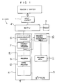
- Fig. 1 is a block diagram of a program control system according to the present invention when it is applied to an IC card.
- 1 is an input contact
- 2 is a MPU
- 3 is a RAM (random access memory)
- 4 is a mask ROM
- 5 is a PROM
- 6 to 12 are program areas in which several kinds of program are stored, respectively.
- the MPU 2 serves to execute, in accordance with the programs 6 to 12 stored in the respective program areas of the mask ROM 4, start management, control of the input contact 1, and the processing for user data and/or commands and a code number using the RAM 3.
- the PROM 5 may be e.g. an EEPROM having a data area with the storage capacity of about 8 K bytes within which a priority control management table 10 and a program area 11 are partially located.
- the RAM 3 may have the storage capacity of about 256 bytes.
- DES data encryption standard
- T 0, etc.
- the control program base on this protocol will be stored in the PROM 5 such as an EEPROM.
- a write program 12 is previously stored in a specific area of the mask ROM 4; the MPU 2, when receiving a command of writing an alternative program, will execute the write program 12.
- a priority control program 7 is previously stored in the mask ROM 4. Now it is assumed that the priority control program 7 is stored in a predetermined program area of the mask ROM 4.
- a communication program 6 for controlling the input contact 1 is stored in another area of the mask ROM 4 and the program 9 for each user is stored in the program area 8.
- the program 9 for each user includes file management (R/W) of data stored in the PROM 5, directory management, lock/unlock of a card, checking PIN (code number), etc.
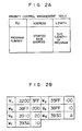
- priority control management table is composed of a program number for identifying each program, the base address of the section of storing the program and data indicative of the size of the program.
- the program number of each program is arranged to be equal with program number of a corresponding program stored in program area 8.
- the program of the program No. 1 is stored in the area starting from the address of 3200 (in a hexadecimal notation) of the PROM 5 and has the size corresponding to the address of 3FF.
- the MPU 2 receives a write command, a program following it, a designated address in the program area and a command number of starting the program (Step 100). Then the MPU 2 shifts its control operation to the write program 12 (Step 110). Thereafter, on the basis of the write program 12, the MPU 2 prepares the priority management table 10 and also writes the alternative program at the designated address in the program area 11 (Step 120). Thus, if a search is made of whether or not each command input from the reader/writer is stored on the priority control management table 10, the specific program stored can be started.
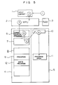
- Fig. 5 shows the flow of operations ( 1 , 2 %) in the case where the program corresponding to the received command is stored in the PROM 5.
- the operation flow in Fig. 5 will be explained with reference to the flowchart of Fig. 7 showing changes in the control state of the MPU 2.
- Step 200 when the IC card is connected with the reader/writer, the IC card is initialized in the processing of a communication program (Step 200).
- a command (Fig. 5 1 ) from the reader/writer is input to the MPU 2 through the input contact 1 (Fig. 5 2 ) in a stand-by state (Fig. 5 3 ; Fig. 7 Step 200).
- the MPU 2 reads the communication program 6 (Fig. 5 4 ) stored in the mask ROM 4, and executes it to place the input contact 1 in a data transmission/ reception enabling state for the reader/writer.
- the MPU 2 reads the priority control program 7 (Fig. 5 5 ) stored in the mask ROM 4 and executes it to search the program number ( 1, 2, ... in Fig.
- the same program number is allotted to the predetermined program stored in the program area 8 in the mask ROM 4 and to the alternative program stored in the PROM 5 therefor in view of user's convenience so that after the alternative program is once stored, it will be automatically operated.
- the alternative program corresponding to a change in the program 9 in the mask ROM 4 has been stored in the program area 11 in the PROM 5.
- the MPU 2 necessarily executes the alternative program, corresponding to the change in the program module 9, stored in the program area 11 in the mask ROM 5.
- the MPU 2 will preferentially execute the program stored in the PROM 5 with the aid of the priority control program 7.
- Fig. 6 shows the flow of operations ( 1 , 2 %) in the case where the program corresponding to the received command is not stored in the PROM 5.
- the operation flow in Fig. 5 will be explained with reference to the flowchart of Fig. 7.
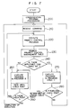
- the MPU 2 when the MPU 2 receives a command from the reader/writer (Fig. 7 Step 210), it executes the communication program 6 stored in the mask ROM 4 (Fig. 6 1 - 4 ). Thereafter, the MPU 2 executes the priority control program 7 (Fig. 6 5 ) stored in the mask ROM 4 to search the program number corresponding to the received command on the priority control management table 10 stored in the PROM 5 (Fig. 7 Step 230). In this case, it is assumed that there is no alternative program for the program previously stored in the program area 8 of the mask ROM 4. When the MPU 2 decides this, it starts to search the program in the program area 8 (Fig. 6 6 ), and reads the program in the program area corresponding to the received command and executes it (Fig. 6 7 , Fig. 7 Step 250).
- the MPU 2 executes the priority control program 7 (Step 220) to search the priority control management table 10 (step 230). If the presence of the command number corresponding to the check point as a result of checking is decided (step 240), the MPU 2 executes the corresponding alternative program stored in the program area 11. Thereafter, if the execution of the program due to the check point is decided in Step 280, the process at issue is returned to execution of the original program in Step 250 to advance the next step at the check point. Thus, if the check point as shown in Fig.
- the MPU executes the program stored in the PROM 5 prior to the program with same number as the former stored in the mask ROM 4; only if there is no corresponding program in the PROM 5, the program stored in the mask ROM 4 will be executed. Therefore, if with all necessary programs stored in the mask ROM 4, an alternative program (relative to modification of the original program using the command number (check point), addition of some programs, and rewrite of the entire program using the actuating command itself of the original program) is stored in the PROM 5 as necessity requires, this alternative program will be preferentially executed.
- the alternative program for the program stored in the mask ROM 4 is stored in the PROM 5, the alternative program will be necessarily executed in place of the program stored in the mask ROM 4.
- the present invention can easily deal with requests of modification, addition and replacement of a program in an IC card.
- the mask ROM can be effectively used with improved use efficiency. Since the storage capacity required for program modification, addition and replacement is greatly limited, the storage capacity in which user data can be stored in the PROM 5 is not particularly restrained.
- the communication can be changed by replacing the communication program processing (Step 200) in Fig. 7 by the sub-routine processing as shown in Fig. 8 which will be carried out in the following process.
- Step 200 when an initializing signal is received from the reader/writer (step 200), another priority control program located in the sub-routine is executed (Step 202) to search the priority control management table 10 (Step 203). If the command number of the control program corresponding to the communication system at issue is present on the priority control management table 10 (Step 204), the corresponding control program stored in the program area 11 will be executed (Step 206). If not, the communication control will be implemented using the communication program of the original communication system previously stored in the mask ROM 4. Thus, also in the case of changing the communication program, in accordance with the procedure shown in Fig. 3, the same command number as the command number actuating the original communication system may be stored on the priority control management table 10 and also an alternative communication program may be stored in the program area 11.
- the data to be stored in the PROM 5 can be managed using the priority control management table 10 as shown in Figs. 2A and 2B.
- the data and the programs may be distinguished in such a manner that they are labelled with distinguishable symbols (e.g. $ for the data and for the program).
- the areas for storing the programs and the data may be previously sectioned; in the case of managing both data and programs, the programs and data may be stored without distinguishing them from each other from the one side of the PROM in the order of their inputting.
- all the data stored in the PROM 5 may be once read out and thereafter stored in their new layout with a new program to be added.
Landscapes
- Physics & Mathematics (AREA)
- General Physics & Mathematics (AREA)
- Engineering & Computer Science (AREA)
- Business, Economics & Management (AREA)
- Microelectronics & Electronic Packaging (AREA)
- Computer Networks & Wireless Communication (AREA)
- Accounting & Taxation (AREA)
- Strategic Management (AREA)
- General Business, Economics & Management (AREA)
- Theoretical Computer Science (AREA)
- Stored Programmes (AREA)
- Read Only Memory (AREA)
Claims (7)
- Programmsteuerungssystem für einen tragbaren Datenspeicher, das umfaßt:Eine Hauptprozessoreinheit MPU(2) zum Starten und Abarbeiten eines internen Programms in Abhängigkeit von einem Eingabe/Ausgabe-Anfragesignal von einer vorgegebenen externen Vorrichtung;einen ersten Speicher (4), der ein Festwertspeicher für die Speicherung nicht änderbarer Fixwertprogramme (9, 12) ist, auf die von der besagten MPU zugegriffen werden soll; undeinen zweiten Speicher (5) zur Speicherung alternativer Programme und welche geschrieben oder gelesen werden können durch die besagte MPU;dadurch gekennzeichnet, daß:der besagte zweite Speicher (5) eine Prioritätsverwaltungstabelle (10) zur Speicherung von Indexinformation der besagten alternativen Programme in dem besagten zweiten Speicher und einen Programmbereich (11) zur Speicherung der besagten alternativen Programme gemäß den besagten Indexinformationen in dem besagten zweiten Speicher umfaßt,eine Prioritätssteuerung (7) auf Aufforderung zur Ausführung des besagten internen Programms die besagte Prioritätsverwaltungstabelle (10) nach Indexinformation durchsucht, die dem auszuführenden Programm entspricht, und bei Vorhandensein dieser Indexinformation in dem besagten zweiten Speicher die besagte MPU anweist, das alternative Programm in dem besagten Programmbereich (11), das durch die besagte Indexinformation bezeichnet ist, auszuführen, und im gegenteiligen Fall die besagte MPU anweist, das dazugehörige Festwertprogramm (9, 12) in dem besagten ersten Speicher (4) auszuführen.
- Programmsteuerungssystem nach Anspruch 1, bei dem ein in dem besagten zweiten Speicher (5) zu speicherndes alternatives Programm ein teilweise hinzugefügtes oder verbessertes Programm eines Festwertprogramms (9, 12) in dem besagten ersten Speicher ist.
- Programmsteuerungssysten nach Anspruch 1 oder 2, bei dem die besagte Prioritätsverwaltungstabelle außerdem eine Basisadresse für jedes alternative Programm umfaßt und die besagte MPU (2) ein alternatives Programm in Abhängigkeit von dessen Basisadresse ausführt.
- Programmsteuerungssystem nach Anspruch 1, 2 oder 3, bei dem ein Festwertprogramm (9, 12) zunächst einen Prüfschritt mit vorgegebener Identifizierungsinformation umfaßt, und wenn die besagte MPU den besagten Prüfschritt bei der Abarbeitung des besagten Festwertprogramms erreicht, sucht die besagte Prioritätssteuerung die besagte Prioritätsverwaltungstabelle durch und wenn Indexinformation entsprechend der besagten Identifizierungsinformation vorliegt, führt die besagte MPU das entsprechende alternative Programm durch.
- Programmsteuerungssystem nach Anspruch 4, bei dem nach Ausführung des besagten entsprechenden alternativen Programms die besagte MPU (2), die Ausführung des besagten Festwertprogramms (9, 12) wieder in dem Teil aufnimmt, der dessen Prüfschritt folgt.
- Programmsteuerungssystem nach Anspruch 1, 2, 3, 4 oder 5, bei dem der besagte tragbare Datenspeicher Schreibvorrichtungen (12) zum Schreiben eines alternativen Programms in dem besagten zweiten Speicher (5) umfaßt; und die besagte Schreibvorrichtung in Abhängigkeit von einem Schreibbefehl von der besagten externen Vorrichtung die Indexinformation des alternativen Programms im besagten zweiten Speicher (5) der besagten Prioritätsverwaltungstabelle (10) speichert und das Programm in dem besagten Programmbereich (11) des zweiten Speichers (5) speichert.
- IC-Karte mit einem Programmsteuerungssystem nach einem der vorangehenden Ansprüche.
Applications Claiming Priority (2)
| Application Number | Priority Date | Filing Date | Title |
|---|---|---|---|
| JP35096/90 | 1990-02-17 | ||
| JP2035096A JPH03240127A (ja) | 1990-02-17 | 1990-02-17 | プログラム制御システム |
Publications (2)
| Publication Number | Publication Date |
|---|---|
| EP0451936A1 EP0451936A1 (de) | 1991-10-16 |
| EP0451936B1 true EP0451936B1 (de) | 1996-12-27 |
Family
ID=12432415
Family Applications (1)
| Application Number | Title | Priority Date | Filing Date |
|---|---|---|---|
| EP91301100A Expired - Lifetime EP0451936B1 (de) | 1990-02-17 | 1991-02-12 | Programmsteuersystem für eine tragbare Datenspeichervorrichtung |
Country Status (4)
| Country | Link |
|---|---|
| US (1) | US5252812A (de) |
| EP (1) | EP0451936B1 (de) |
| JP (1) | JPH03240127A (de) |
| DE (1) | DE69123775T2 (de) |
Cited By (11)
| Publication number | Priority date | Publication date | Assignee | Title |
|---|---|---|---|---|
| US6164549A (en) | 1997-05-15 | 2000-12-26 | Mondex International Limited | IC card with shell feature |
| US6220510B1 (en) | 1997-05-15 | 2001-04-24 | Mondex International Limited | Multi-application IC card with delegation feature |
| US6328217B1 (en) | 1997-05-15 | 2001-12-11 | Mondex International Limited | Integrated circuit card with application history list |
| US6385723B1 (en) | 1997-05-15 | 2002-05-07 | Mondex International Limited | Key transformation unit for an IC card |
| US6488211B1 (en) | 1997-05-15 | 2002-12-03 | Mondex International Limited | System and method for flexibly loading in IC card |
| US6575372B1 (en) | 1997-02-21 | 2003-06-10 | Mondex International Limited | Secure multi-application IC card system having selective loading and deleting capability |
| US6736325B1 (en) | 1998-01-22 | 2004-05-18 | Mondex International Limited | Codelets |
| US6742120B1 (en) | 1998-02-03 | 2004-05-25 | Mondex International Limited | System and method for controlling access to computer code in an IC card |
| US6761319B2 (en) | 1998-01-22 | 2004-07-13 | Mondex International Limited | Configuration of IC card |
| US7469339B2 (en) | 1997-05-15 | 2008-12-23 | Multos Limited | Secure multiple application card system and process |
| US7523495B2 (en) | 2006-04-19 | 2009-04-21 | Multos Limited | Methods and systems for IC card application loading |
Families Citing this family (35)
| Publication number | Priority date | Publication date | Assignee | Title |
|---|---|---|---|---|
| GB9019423D0 (en) * | 1990-09-06 | 1990-10-24 | Gen Motors Luxembourg Operatio | Electronic controller for vehicle |
| FR2667417B1 (fr) * | 1990-10-02 | 1992-11-27 | Gemplus Card Int | Carte a microprocesseur concue pour recevoir des programmes multiples en memoire programmable. |
| JP2724046B2 (ja) * | 1991-02-07 | 1998-03-09 | 富士写真フイルム株式会社 | Icメモリカードシステム |
| FR2683357A1 (fr) * | 1991-10-30 | 1993-05-07 | Philips Composants | Microcircuit pour carte a puce a memoire programmable protegee. |
| EP0583723A1 (de) * | 1992-08-20 | 1994-02-23 | THOMSON multimedia | Karte, Kartenleser und Verfahren zur Protokollauswahl |
| EP0583526A1 (de) * | 1992-08-20 | 1994-02-23 | THOMSON multimedia | Karte, Kartenleser und Verfahren zur Protokollauswahl |
| WO1994010657A1 (en) * | 1992-10-26 | 1994-05-11 | Intellect Australia Pty. Ltd. | Host and user transaction system |
| JP3480958B2 (ja) * | 1993-02-19 | 2003-12-22 | 富士通株式会社 | 文字ファイルアクセス方式 |
| JP3568970B2 (ja) * | 1993-04-12 | 2004-09-22 | 株式会社東芝 | Icカード発行装置 |
| US5555389A (en) * | 1993-07-07 | 1996-09-10 | Hitachi, Ltd. | Storage controller for performing dump processing |
| JP3662946B2 (ja) * | 1993-09-22 | 2005-06-22 | 株式会社東芝 | ファイル管理方式および携帯可能電子装置 |
| US6145739A (en) * | 1993-10-26 | 2000-11-14 | Intellect Australia Pty Ltd. | System and method for performing transactions and an intelligent device therefor |
| US5679944A (en) | 1994-06-15 | 1997-10-21 | Dallas Semiconductor Corporation | Portable electronic module having EPROM memory, systems and processes |
| DE4425388B4 (de) * | 1994-07-19 | 2005-07-21 | Robert Bosch Gmbh | Steuergerät |
| DE4440127B4 (de) * | 1994-11-10 | 2007-11-08 | Robert Bosch Gmbh | Steuergerät |
| US5918006A (en) * | 1994-12-20 | 1999-06-29 | Canon Kabushiki Kaisha | Communication device provided with a storage medium for storing a control program |
| JPH0962583A (ja) * | 1995-08-24 | 1997-03-07 | Mitsubishi Electric Corp | データ処理装置 |
| US5832263A (en) * | 1996-03-15 | 1998-11-03 | Digidox, Inc. | System and method for in-place modification of information recorded in read-only storage using modifiable non-volatile storage associated with an agent |
| DE19718115A1 (de) * | 1996-12-23 | 1998-06-25 | Ccs Chipcard & Comm Syst Gmbh | Chipkarte und Verfahren zur Verwendung der Chipkarte |
| JP3689213B2 (ja) | 1997-01-21 | 2005-08-31 | ローム株式会社 | 非接触型icカード |
| US6230267B1 (en) | 1997-05-15 | 2001-05-08 | Mondex International Limited | IC card transportation key set |
| CA2294469A1 (en) * | 1997-06-23 | 1998-12-30 | Siemens Aktiengesellschaft | Chip card for executing non-modifiable system program routines and their associated replacement program routines, and a method for operating the chip card |
| JPH11191149A (ja) | 1997-12-26 | 1999-07-13 | Oki Electric Ind Co Ltd | Icカード用lsiおよびその使用方法 |
| WO1999040548A1 (en) * | 1998-02-06 | 1999-08-12 | Mondex International Limited | Configuration of ic card |
| US7373521B1 (en) * | 1999-02-17 | 2008-05-13 | Sony Corporation | Semiconductor IC, information processing method, information processing device, and program storage medium |
| US6493616B1 (en) * | 1999-08-13 | 2002-12-10 | Clark Equipment Company | Diagnostic and control unit for power machine |
| GB9925227D0 (en) | 1999-10-25 | 1999-12-22 | Internet Limited | Data storage retrieval and access system |
| US7539828B2 (en) * | 2000-08-08 | 2009-05-26 | Faronics Corporation | Method and system for automatically preserving persistent storage |
| DE60121212T2 (de) * | 2000-11-20 | 2006-11-09 | Matsushita Electric Industrial Co., Ltd., Kadoma | Kontaktlose lese-/schreibvorrichtung, informationsübermittlungssystem damit und verwaltungssystem damit |
| KR20040101293A (ko) | 2002-03-13 | 2004-12-02 | 마츠시타 덴끼 산교 가부시키가이샤 | 보안장치 |
| US7065605B2 (en) * | 2003-07-28 | 2006-06-20 | Seagate Technology Llc | Dynamic mask-ROM register patching |
| JP4580660B2 (ja) * | 2004-02-19 | 2010-11-17 | 大日本印刷株式会社 | Romにアプリケーションを実装したマルチアプリケーションicカードおよびアプリケーションプログラム |
| JP5034460B2 (ja) * | 2006-11-29 | 2012-09-26 | 大日本印刷株式会社 | 情報処理装置とそのプログラム、情報処理装置の製造方法、及び、情報処理装置の使用方法 |
| JP2008165744A (ja) * | 2006-12-07 | 2008-07-17 | Semiconductor Energy Lab Co Ltd | 半導体装置 |
| JP5795921B2 (ja) * | 2011-09-21 | 2015-10-14 | 株式会社東芝 | Icカード、携帯可能電子装置、icカードの制御方法 |
Family Cites Families (8)
| Publication number | Priority date | Publication date | Assignee | Title |
|---|---|---|---|---|
| US4028684A (en) * | 1975-10-16 | 1977-06-07 | Bell Telephone Laboratories, Incorporated | Memory patching circuit with repatching capability |
| US4506346A (en) * | 1982-12-01 | 1985-03-19 | At&T Bell Laboratories | Programmable cartridge telephone communication system |
| US4703416A (en) * | 1982-12-10 | 1987-10-27 | American Telephone And Telegraph Company | Apparatus for locating programs resident on a cartridge of a cartridge programmable communication system |
| US4835686A (en) * | 1985-05-29 | 1989-05-30 | Kabushiki Kaisha Toshiba | Cache system adopting an LRU system, and magnetic disk controller incorporating it |
| US4829169A (en) * | 1985-07-01 | 1989-05-09 | Toppan Moore Company, Inc. | IC card having state marker for record access |
| DE3743639A1 (de) * | 1986-12-24 | 1988-07-07 | Mitsubishi Electric Corp | Ic-karte und system zur ueberpruefung ihrer funktionstuechtigkeit |
| DE68927361T4 (de) * | 1988-08-12 | 1999-11-04 | Hitachi Maxell, Ltd. | Chipkarte und Verfahren zum Wiedereinschreiben ihres Programmes |
| US5136700A (en) * | 1989-12-22 | 1992-08-04 | Digital Equipment Corporation | Apparatus and method for reducing interference in two-level cache memories |
-
1990
- 1990-02-17 JP JP2035096A patent/JPH03240127A/ja active Pending
-
1991
- 1991-02-06 US US07/651,545 patent/US5252812A/en not_active Expired - Fee Related
- 1991-02-12 EP EP91301100A patent/EP0451936B1/de not_active Expired - Lifetime
- 1991-02-12 DE DE69123775T patent/DE69123775T2/de not_active Expired - Fee Related
Cited By (22)
| Publication number | Priority date | Publication date | Assignee | Title |
|---|---|---|---|---|
| US7689826B2 (en) | 1997-02-21 | 2010-03-30 | Multos Limited | Flexibly loading a tamper resistant module |
| US7702908B2 (en) | 1997-02-21 | 2010-04-20 | Multos Limited | Tamper resistant module certification authority |
| US7734923B2 (en) | 1997-02-21 | 2010-06-08 | Multos Limited | Key transformation unit for a tamper resistant module |
| US7730310B2 (en) | 1997-02-21 | 2010-06-01 | Multos Limited | Key transformation unit for a tamper resistant module |
| US7730312B2 (en) | 1997-02-21 | 2010-06-01 | Multos Limted | Tamper resistant module certification authority |
| US6575372B1 (en) | 1997-02-21 | 2003-06-10 | Mondex International Limited | Secure multi-application IC card system having selective loading and deleting capability |
| US6659354B2 (en) | 1997-02-21 | 2003-12-09 | Mondex International Limited | Secure multi-application IC card system having selective loading and deleting capability |
| US7730311B2 (en) | 1997-02-21 | 2010-06-01 | Multos Limited | Key transformation unit for a tamper resistant module |
| US7707408B2 (en) | 1997-02-21 | 2010-04-27 | Multos Limited | Key transformation unit for a tamper resistant module |
| US7669055B2 (en) | 1997-02-21 | 2010-02-23 | Multos Limited | Key transformation unit for a tamper resistant module |
| US7584358B2 (en) | 1997-02-21 | 2009-09-01 | Multos Limited | Tamper resistant module certification authority |
| US7469339B2 (en) | 1997-05-15 | 2008-12-23 | Multos Limited | Secure multiple application card system and process |
| US6742715B2 (en) | 1997-05-15 | 2004-06-01 | Mondex International Limited | System and method for flexibly loading an IC card |
| US6220510B1 (en) | 1997-05-15 | 2001-04-24 | Mondex International Limited | Multi-application IC card with delegation feature |
| US6164549A (en) | 1997-05-15 | 2000-12-26 | Mondex International Limited | IC card with shell feature |
| US6488211B1 (en) | 1997-05-15 | 2002-12-03 | Mondex International Limited | System and method for flexibly loading in IC card |
| US6385723B1 (en) | 1997-05-15 | 2002-05-07 | Mondex International Limited | Key transformation unit for an IC card |
| US6328217B1 (en) | 1997-05-15 | 2001-12-11 | Mondex International Limited | Integrated circuit card with application history list |
| US6761319B2 (en) | 1998-01-22 | 2004-07-13 | Mondex International Limited | Configuration of IC card |
| US6736325B1 (en) | 1998-01-22 | 2004-05-18 | Mondex International Limited | Codelets |
| US6742120B1 (en) | 1998-02-03 | 2004-05-25 | Mondex International Limited | System and method for controlling access to computer code in an IC card |
| US7523495B2 (en) | 2006-04-19 | 2009-04-21 | Multos Limited | Methods and systems for IC card application loading |
Also Published As
| Publication number | Publication date |
|---|---|
| DE69123775T2 (de) | 1997-07-10 |
| EP0451936A1 (de) | 1991-10-16 |
| JPH03240127A (ja) | 1991-10-25 |
| US5252812A (en) | 1993-10-12 |
| DE69123775D1 (de) | 1997-02-06 |
Similar Documents
| Publication | Publication Date | Title |
|---|---|---|
| EP0451936B1 (de) | Programmsteuersystem für eine tragbare Datenspeichervorrichtung | |
| US5093785A (en) | Portable electronic device with memory having data pointers and circuitry for determining whether a next unwritten memory location exist | |
| JP2537199B2 (ja) | Icカ―ド | |
| US4988855A (en) | Portable electronic apparatus | |
| EP1450299B1 (de) | Tragbares informationsaufzeichnungsmedium | |
| US20100070707A1 (en) | Portable electronic device and data processing method in portable electronic device | |
| US7775423B2 (en) | Portable electronic device and control method of portable electronic device | |
| EP2642422B1 (de) | Ic-karte und ic-kartensteuerverfahren | |
| EP0354793A2 (de) | Chipkarte und Verfahren zum Wiedereinschreiben ihres Programmes | |
| JPH06282471A (ja) | ファイル管理方式 | |
| JP4090350B2 (ja) | Icカード | |
| EP0950982B1 (de) | Tragbares elektronisches Gerät | |
| JP4742469B2 (ja) | 複数のosを用いるicカード、icカード処理装置および処理方法 | |
| US20020004864A1 (en) | Control method and electronic device | |
| US6415371B1 (en) | Storage system, storage device, storage medium controller, access device, method for protecting data, storage medium and computer data signal | |
| JP2005011161A (ja) | Icカード及びicカードプログラム | |
| JP2010211516A (ja) | 携帯可能電子装置および携帯可能電子装置におけるアクセス制御方法 | |
| KR100399603B1 (ko) | 스마트 카드와 이의 os 프로그램 저장/삭제 및 실행방법 | |
| US7296289B2 (en) | Setting or changing an access condition for an access management apparatus and method of a portable electronic device | |
| JP3017736B2 (ja) | 携帯可能電子装置 | |
| JP2005011147A (ja) | Icカード及びicカードプログラム | |
| JP4318494B2 (ja) | Icカード及びicカードプログラム | |
| JP4059452B2 (ja) | Icカード | |
| JP2002024790A (ja) | 情報処理システム、携帯可能電子装置、及びキー変更方法 | |
| JP4026796B2 (ja) | コマンド振り分け機能付きicカード |
Legal Events
| Date | Code | Title | Description |
|---|---|---|---|
| PUAI | Public reference made under article 153(3) epc to a published international application that has entered the european phase |
Free format text: ORIGINAL CODE: 0009012 |
|
| AK | Designated contracting states |
Kind code of ref document: A1 Designated state(s): DE FR GB |
|
| 17P | Request for examination filed |
Effective date: 19920205 |
|
| 17Q | First examination report despatched |
Effective date: 19940405 |
|
| GRAG | Despatch of communication of intention to grant |
Free format text: ORIGINAL CODE: EPIDOS AGRA |
|
| GRAH | Despatch of communication of intention to grant a patent |
Free format text: ORIGINAL CODE: EPIDOS IGRA |
|
| GRAH | Despatch of communication of intention to grant a patent |
Free format text: ORIGINAL CODE: EPIDOS IGRA |
|
| GRAA | (expected) grant |
Free format text: ORIGINAL CODE: 0009210 |
|
| AK | Designated contracting states |
Kind code of ref document: B1 Designated state(s): DE FR GB |
|
| ET | Fr: translation filed | ||
| REF | Corresponds to: |
Ref document number: 69123775 Country of ref document: DE Date of ref document: 19970206 |
|
| PLBE | No opposition filed within time limit |
Free format text: ORIGINAL CODE: 0009261 |
|
| STAA | Information on the status of an ep patent application or granted ep patent |
Free format text: STATUS: NO OPPOSITION FILED WITHIN TIME LIMIT |
|
| 26N | No opposition filed | ||
| REG | Reference to a national code |
Ref country code: GB Ref legal event code: IF02 |
|
| PGFP | Annual fee paid to national office [announced via postgrant information from national office to epo] |
Ref country code: DE Payment date: 20030430 Year of fee payment: 13 |
|
| PGFP | Annual fee paid to national office [announced via postgrant information from national office to epo] |
Ref country code: FR Payment date: 20031217 Year of fee payment: 14 |
|
| PGFP | Annual fee paid to national office [announced via postgrant information from national office to epo] |
Ref country code: GB Payment date: 20040211 Year of fee payment: 14 |
|
| PG25 | Lapsed in a contracting state [announced via postgrant information from national office to epo] |
Ref country code: DE Free format text: LAPSE BECAUSE OF NON-PAYMENT OF DUE FEES Effective date: 20040901 |
|
| PG25 | Lapsed in a contracting state [announced via postgrant information from national office to epo] |
Ref country code: GB Free format text: LAPSE BECAUSE OF NON-PAYMENT OF DUE FEES Effective date: 20050212 |
|
| GBPC | Gb: european patent ceased through non-payment of renewal fee |
Effective date: 20050212 |
|
| PG25 | Lapsed in a contracting state [announced via postgrant information from national office to epo] |
Ref country code: FR Free format text: LAPSE BECAUSE OF NON-PAYMENT OF DUE FEES Effective date: 20051031 |
|
| REG | Reference to a national code |
Ref country code: FR Ref legal event code: ST Effective date: 20051031 |