EP0451982A2 - Developer unit - Google Patents
Developer unit Download PDFInfo
- Publication number
- EP0451982A2 EP0451982A2 EP91302543A EP91302543A EP0451982A2 EP 0451982 A2 EP0451982 A2 EP 0451982A2 EP 91302543 A EP91302543 A EP 91302543A EP 91302543 A EP91302543 A EP 91302543A EP 0451982 A2 EP0451982 A2 EP 0451982A2
- Authority
- EP
- European Patent Office
- Prior art keywords
- developer
- developer carrier
- carrier
- conductive
- constraining member
- Prior art date
- Legal status (The legal status is an assumption and is not a legal conclusion. Google has not performed a legal analysis and makes no representation as to the accuracy of the status listed.)
- Withdrawn
Links
- 229920005989 resin Polymers 0.000 claims description 69
- 239000011347 resin Substances 0.000 claims description 69
- 229910052751 metal Inorganic materials 0.000 claims description 60
- 239000002184 metal Substances 0.000 claims description 60
- 238000000034 method Methods 0.000 claims description 39
- 230000008569 process Effects 0.000 claims description 35
- 239000004020 conductor Substances 0.000 claims description 15
- 238000004519 manufacturing process Methods 0.000 claims description 10
- 239000002131 composite material Substances 0.000 claims description 6
- 238000005498 polishing Methods 0.000 claims description 6
- 239000012858 resilient material Substances 0.000 claims description 5
- 230000001747 exhibiting effect Effects 0.000 claims description 4
- 238000007493 shaping process Methods 0.000 claims description 2
- 238000003756 stirring Methods 0.000 description 20
- 238000011161 development Methods 0.000 description 13
- OKTJSMMVPCPJKN-UHFFFAOYSA-N Carbon Chemical compound [C] OKTJSMMVPCPJKN-UHFFFAOYSA-N 0.000 description 12
- 229910052799 carbon Inorganic materials 0.000 description 12
- 230000008859 change Effects 0.000 description 12
- 230000009471 action Effects 0.000 description 10
- 239000011248 coating agent Substances 0.000 description 9
- 238000000576 coating method Methods 0.000 description 9
- 239000006185 dispersion Substances 0.000 description 9
- 239000000945 filler Substances 0.000 description 9
- 239000000843 powder Substances 0.000 description 9
- 239000004411 aluminium Substances 0.000 description 7
- 229910052782 aluminium Inorganic materials 0.000 description 7
- XAGFODPZIPBFFR-UHFFFAOYSA-N aluminium Chemical compound [Al] XAGFODPZIPBFFR-UHFFFAOYSA-N 0.000 description 7
- 230000000694 effects Effects 0.000 description 7
- 238000005192 partition Methods 0.000 description 7
- 230000002093 peripheral effect Effects 0.000 description 7
- BQCADISMDOOEFD-UHFFFAOYSA-N Silver Chemical compound [Ag] BQCADISMDOOEFD-UHFFFAOYSA-N 0.000 description 6
- 239000000853 adhesive Substances 0.000 description 6
- 230000001070 adhesive effect Effects 0.000 description 6
- 239000000835 fiber Substances 0.000 description 6
- 239000000463 material Substances 0.000 description 6
- 230000015572 biosynthetic process Effects 0.000 description 5
- 239000007787 solid Substances 0.000 description 5
- 239000010935 stainless steel Substances 0.000 description 5
- 229910001220 stainless steel Inorganic materials 0.000 description 5
- 239000003522 acrylic cement Substances 0.000 description 4
- 238000010276 construction Methods 0.000 description 4
- 238000000151 deposition Methods 0.000 description 4
- 230000005684 electric field Effects 0.000 description 4
- 229920006332 epoxy adhesive Polymers 0.000 description 4
- 230000002349 favourable effect Effects 0.000 description 4
- 230000009467 reduction Effects 0.000 description 4
- 229920002379 silicone rubber Polymers 0.000 description 4
- 239000004945 silicone rubber Substances 0.000 description 4
- 229910052709 silver Inorganic materials 0.000 description 4
- 239000004332 silver Substances 0.000 description 4
- 229910000906 Bronze Inorganic materials 0.000 description 3
- OAICVXFJPJFONN-UHFFFAOYSA-N Phosphorus Chemical compound [P] OAICVXFJPJFONN-UHFFFAOYSA-N 0.000 description 3
- 229910000639 Spring steel Inorganic materials 0.000 description 3
- 239000010974 bronze Substances 0.000 description 3
- 230000015556 catabolic process Effects 0.000 description 3
- KUNSUQLRTQLHQQ-UHFFFAOYSA-N copper tin Chemical compound [Cu].[Sn] KUNSUQLRTQLHQQ-UHFFFAOYSA-N 0.000 description 3
- 230000008021 deposition Effects 0.000 description 3
- 239000004677 Nylon Substances 0.000 description 2
- 229920000297 Rayon Polymers 0.000 description 2
- 229920006311 Urethane elastomer Polymers 0.000 description 2
- 238000005299 abrasion Methods 0.000 description 2
- 230000004308 accommodation Effects 0.000 description 2
- 229940090961 chromium dioxide Drugs 0.000 description 2
- IAQWMWUKBQPOIY-UHFFFAOYSA-N chromium(4+);oxygen(2-) Chemical compound [O-2].[O-2].[Cr+4] IAQWMWUKBQPOIY-UHFFFAOYSA-N 0.000 description 2
- AYTAKQFHWFYBMA-UHFFFAOYSA-N chromium(IV) oxide Inorganic materials O=[Cr]=O AYTAKQFHWFYBMA-UHFFFAOYSA-N 0.000 description 2
- 230000007423 decrease Effects 0.000 description 2
- 230000007547 defect Effects 0.000 description 2
- 238000009826 distribution Methods 0.000 description 2
- 238000002474 experimental method Methods 0.000 description 2
- 238000002347 injection Methods 0.000 description 2
- 239000007924 injection Substances 0.000 description 2
- 239000011810 insulating material Substances 0.000 description 2
- 239000000203 mixture Substances 0.000 description 2
- 229920001778 nylon Polymers 0.000 description 2
- -1 polyethylene Polymers 0.000 description 2
- 239000002964 rayon Substances 0.000 description 2
- 238000012546 transfer Methods 0.000 description 2
- 229920000178 Acrylic resin Polymers 0.000 description 1
- 239000004925 Acrylic resin Substances 0.000 description 1
- RYGMFSIKBFXOCR-UHFFFAOYSA-N Copper Chemical compound [Cu] RYGMFSIKBFXOCR-UHFFFAOYSA-N 0.000 description 1
- JOYRKODLDBILNP-UHFFFAOYSA-N Ethyl urethane Chemical compound CCOC(N)=O JOYRKODLDBILNP-UHFFFAOYSA-N 0.000 description 1
- 229920000877 Melamine resin Polymers 0.000 description 1
- 239000004640 Melamine resin Substances 0.000 description 1
- 239000002033 PVDF binder Substances 0.000 description 1
- ISWSIDIOOBJBQZ-UHFFFAOYSA-N Phenol Chemical compound OC1=CC=CC=C1 ISWSIDIOOBJBQZ-UHFFFAOYSA-N 0.000 description 1
- 239000004698 Polyethylene Substances 0.000 description 1
- 239000004743 Polypropylene Substances 0.000 description 1
- 239000004793 Polystyrene Substances 0.000 description 1
- 229920005830 Polyurethane Foam Polymers 0.000 description 1
- XSQUKJJJFZCRTK-UHFFFAOYSA-N Urea Chemical compound NC(N)=O XSQUKJJJFZCRTK-UHFFFAOYSA-N 0.000 description 1
- 229920001807 Urea-formaldehyde Polymers 0.000 description 1
- 238000005054 agglomeration Methods 0.000 description 1
- 230000002776 aggregation Effects 0.000 description 1
- 238000010420 art technique Methods 0.000 description 1
- 238000005513 bias potential Methods 0.000 description 1
- 239000004202 carbamide Substances 0.000 description 1
- 239000000969 carrier Substances 0.000 description 1
- 239000000919 ceramic Substances 0.000 description 1
- 229910052802 copper Inorganic materials 0.000 description 1
- 239000010949 copper Substances 0.000 description 1
- 239000013078 crystal Substances 0.000 description 1
- 238000006731 degradation reaction Methods 0.000 description 1
- 230000000593 degrading effect Effects 0.000 description 1
- 239000003989 dielectric material Substances 0.000 description 1
- 230000003292 diminished effect Effects 0.000 description 1
- 239000002612 dispersion medium Substances 0.000 description 1
- 229920001971 elastomer Polymers 0.000 description 1
- 238000004299 exfoliation Methods 0.000 description 1
- 239000010419 fine particle Substances 0.000 description 1
- 230000000977 initiatory effect Effects 0.000 description 1
- 238000011835 investigation Methods 0.000 description 1
- 238000003475 lamination Methods 0.000 description 1
- 238000003754 machining Methods 0.000 description 1
- 239000006247 magnetic powder Substances 0.000 description 1
- 230000004048 modification Effects 0.000 description 1
- 238000012986 modification Methods 0.000 description 1
- 239000005011 phenolic resin Substances 0.000 description 1
- 229920000728 polyester Polymers 0.000 description 1
- 239000004645 polyester resin Substances 0.000 description 1
- 229920001225 polyester resin Polymers 0.000 description 1
- 229920000573 polyethylene Polymers 0.000 description 1
- 239000002861 polymer material Substances 0.000 description 1
- 229920001155 polypropylene Polymers 0.000 description 1
- 229920005990 polystyrene resin Polymers 0.000 description 1
- 239000004814 polyurethane Substances 0.000 description 1
- 229920003225 polyurethane elastomer Polymers 0.000 description 1
- 239000011496 polyurethane foam Substances 0.000 description 1
- 229920005749 polyurethane resin Polymers 0.000 description 1
- 229920002981 polyvinylidene fluoride Polymers 0.000 description 1
- 239000011148 porous material Substances 0.000 description 1
- 238000012805 post-processing Methods 0.000 description 1
- 238000002360 preparation method Methods 0.000 description 1
- 230000002035 prolonged effect Effects 0.000 description 1
- 230000000717 retained effect Effects 0.000 description 1
- 238000007790 scraping Methods 0.000 description 1
- 238000004544 sputter deposition Methods 0.000 description 1
- 238000003860 storage Methods 0.000 description 1
- 239000000758 substrate Substances 0.000 description 1
- 229920005992 thermoplastic resin Polymers 0.000 description 1
- 229920001187 thermosetting polymer Polymers 0.000 description 1
- 239000010409 thin film Substances 0.000 description 1
Images






Classifications
-
- G—PHYSICS
- G03—PHOTOGRAPHY; CINEMATOGRAPHY; ANALOGOUS TECHNIQUES USING WAVES OTHER THAN OPTICAL WAVES; ELECTROGRAPHY; HOLOGRAPHY
- G03G—ELECTROGRAPHY; ELECTROPHOTOGRAPHY; MAGNETOGRAPHY
- G03G15/00—Apparatus for electrographic processes using a charge pattern
- G03G15/06—Apparatus for electrographic processes using a charge pattern for developing
- G03G15/08—Apparatus for electrographic processes using a charge pattern for developing using a solid developer, e.g. powder developer
- G03G15/0806—Apparatus for electrographic processes using a charge pattern for developing using a solid developer, e.g. powder developer on a donor element, e.g. belt, roller
-
- G—PHYSICS
- G03—PHOTOGRAPHY; CINEMATOGRAPHY; ANALOGOUS TECHNIQUES USING WAVES OTHER THAN OPTICAL WAVES; ELECTROGRAPHY; HOLOGRAPHY
- G03G—ELECTROGRAPHY; ELECTROPHOTOGRAPHY; MAGNETOGRAPHY
- G03G15/00—Apparatus for electrographic processes using a charge pattern
- G03G15/06—Apparatus for electrographic processes using a charge pattern for developing
- G03G15/08—Apparatus for electrographic processes using a charge pattern for developing using a solid developer, e.g. powder developer
- G03G15/0806—Apparatus for electrographic processes using a charge pattern for developing using a solid developer, e.g. powder developer on a donor element, e.g. belt, roller
- G03G15/0812—Apparatus for electrographic processes using a charge pattern for developing using a solid developer, e.g. powder developer on a donor element, e.g. belt, roller characterised by the developer regulating means, e.g. structure of doctor blade
-
- G—PHYSICS
- G03—PHOTOGRAPHY; CINEMATOGRAPHY; ANALOGOUS TECHNIQUES USING WAVES OTHER THAN OPTICAL WAVES; ELECTROGRAPHY; HOLOGRAPHY
- G03G—ELECTROGRAPHY; ELECTROPHOTOGRAPHY; MAGNETOGRAPHY
- G03G15/00—Apparatus for electrographic processes using a charge pattern
- G03G15/06—Apparatus for electrographic processes using a charge pattern for developing
- G03G15/08—Apparatus for electrographic processes using a charge pattern for developing using a solid developer, e.g. powder developer
- G03G15/0806—Apparatus for electrographic processes using a charge pattern for developing using a solid developer, e.g. powder developer on a donor element, e.g. belt, roller
- G03G15/0818—Apparatus for electrographic processes using a charge pattern for developing using a solid developer, e.g. powder developer on a donor element, e.g. belt, roller characterised by the structure of the donor member, e.g. surface properties
-
- G—PHYSICS
- G03—PHOTOGRAPHY; CINEMATOGRAPHY; ANALOGOUS TECHNIQUES USING WAVES OTHER THAN OPTICAL WAVES; ELECTROGRAPHY; HOLOGRAPHY
- G03G—ELECTROGRAPHY; ELECTROPHOTOGRAPHY; MAGNETOGRAPHY
- G03G2215/00—Apparatus for electrophotographic processes
- G03G2215/06—Developing structures, details
- G03G2215/0602—Developer
- G03G2215/0604—Developer solid type
- G03G2215/0614—Developer solid type one-component
- G03G2215/0617—Developer solid type one-component contact development (i.e. the developer layer on the donor member contacts the latent image carrier)
-
- G—PHYSICS
- G03—PHOTOGRAPHY; CINEMATOGRAPHY; ANALOGOUS TECHNIQUES USING WAVES OTHER THAN OPTICAL WAVES; ELECTROGRAPHY; HOLOGRAPHY
- G03G—ELECTROGRAPHY; ELECTROPHOTOGRAPHY; MAGNETOGRAPHY
- G03G2215/00—Apparatus for electrophotographic processes
- G03G2215/06—Developing structures, details
- G03G2215/0634—Developing device
- G03G2215/0636—Specific type of dry developer device
Definitions
- the invention relates to developer units, and in particular, to developer units utilising a non-magnetic single component developer.
- the invention also relates to the manufacture of developer carriers for developer units.
- Prior art techniques to develop an electrostatic latent image which may be formed by an exposure of a uniformly charged photosensitive member in accordance with image information generally include a two component developer process which uses a toner and a carrier, in particular such a process utilising a magnetic brush, which will be hereafter referred to as a two component magnetic brush developing process.
- a two component magnetic brush developing process suffers from practical difficulties including an increased size of the resulting developer unit, difficulty in achieving a stable mixture ratio of toner and carrier and an associated difficulty in charging the toner.
- a magnetic brush developing process utilising a single component developer in which the toner itself exhibits a magnetic property hereafter referred to as a single component magnetic brush developing process
- a single component magnetic brush developing process has been available on the market.
- the single component magnetic brush process presents difficulties in achieving a colour image in view of the fact that the developing powder includes a magnetic powder.
- a developing process utilising a non-magnetic, single component developer (hereafter referred to as a non-magnetic single component developing process), which is still under investigation.
- This process is again categorised into a process in which the development takes place by the contact between a developer and an electrostatic latent image carrier such as a photosensitive member, for example, and another process in which the developer and the latent image carrier are maintained out of contact from each other while the development takes place by causing the developer to fly onto the carrier.
- the former or contact process results in excellent results in improving the image density and the ease of supplying a developer, but suffers from susceptibility to the occurrence of a background fogging which is caused by the contact betweeen the developer and the latent image carrier.
- it exhibits the disadvantage that it cannot be adopted in a single drum, multiple colour, single transfer process which is intended to achieve a simplification of an overall developer unit and a reduction in the cost in producing a colour image, in view of the contacting nature of the process which gives rise to the problem of colour mixture. Accordingly, resort must be had to the latter or non-contact, flying developing process which utilises the non-magnetic single component developer.
- the use of the non-magnetic single component developer may cause a poor image, such as a thinning or braking of the image, unless a supply of developer to the holder, its charging, the formation of a thin layer thereof, conveyance to a developing zone and the flying capability are properly controlled together with a satisfactory achievement of the removal, stirring action and circulation of the developer.
- a conventional developer unit in which a developer is charged and a thin layer is formed simultaneously by means of a constraining member, such as a pressure blade
- the degree to which the developer is charged cannot be stabilised in view of the triboelectric nature of charging, but undergoes a large variation subject to the material and a change in the surface condition of the constraining member, resulting in poor reliability.
- residual developer which remains on the carrier after for developing step cannot be removed from the carrier, and is allowed to be used again in the next following developing step as the carrier rotates. In this manner, difficulties are experienced in achieving a stable charging of the developer and a satisfactory stirring action of the developer.
- a developing bias such as an electric pulse of a a.c. bias
- a gap g between the developer carrier and the electrostatic latent image carrier must be maintained very small; of the order of 0.5 to 0.02 mm.
- a metal developer carrier which is made of a commonly used metal, such as aluminium, stainless steel or the like
- the choice of a high developing bias which is applied to the developer carrier from a high voltage source will cause the liability of the developing bias to discharge, which upon occurrence, reduces the potential of the developer carrier to a point near earth potential, with the consequence that a resulting low bias phenomenon occurs across the entire developer carrier to produce a black traversing pattern running across the background (non-image area) of a copy or the electric breakdown of the air will produce a white dot discharge pattern in the image area, thus causing a degradation in the image quality.
- the choice of a low developing bias cannot assure a satisfactory developing capability.
- a developer unit using a developer carrier which comprises a cylindrical member formed by a conductive resin in which a conductive powder is dispersed and having openings at its opposite ends, to which a pair of end supports carrying stub shafts are coupled, with the resistivity of the conductive resin forming the cylindrical member chosen to be in a range from 104 to 1012 ohms cm with a wall thickness in a range from 0.5 to 3 mm (see, for example JP-A-85/80875.
- the resistivity of the conductive resin suppresses the discharge of the developing bias, and thus the choice of a high applied developing bias cannot result in the appearance of a black traversing pattern in the background (or non-image area) of a copy which might have been otherwise caused by the discharge of the developing bias.
- the occurrence of a discharge pattern in the form of white dots in the image area is also avoided, and the reproducibility of a solid black image is not degraded.
- the construction of the developer carrier which is formed of a conductive resin and which is supported at its opposite ends by the pair of stub supports present difficulty in ensuring the rigidity of the developer carrier and the concentricity of the outer diameter thereof with respect to the axis. This in turn presents difficulty in maintaining a gap between the developer carrier and the latent image carrier to a high accuracy. Any variation in the gap is reflected in non-uniformity of the image density.
- the developer carrier has an outer diameter less that 30 mm or a length greater than 200 mm, sufficient rigidity cannot be ensured, causing a flexure therein.
- a developer unit in which a non-magnetic single-component developer is supplied to the surface of a developer carrier and is formed into a substantially uniform thin layer thereon by means of a constraining member and in which an electrical developing bias is applied to the developer carrier to cause developer to fly across a gap onto an image area of an electrostatic latent image formed on a latent image carrier opposed to the developer carrier, is characterised in that the developer carrier is metallic or comprises a metal core and an electrically conductive yieldable charging member is rotatably disposed in physical contact with the developer carrier, and in that the constraining member is electrically conductive and a high voltage is applied to the charging member and the constraining member as well as the developer carrier, whereby the constraining member charges the developer on the developer holder to a predetermined potential.
- the invention includes a developer unit whose developer carrier comprises a metal case and a conducting resin layer on the core.
- the layer preferably has a thickness from 1.5 to 5mm and a resistivity from 104 to 108 ohm-cm.
- the invention also includes a process of manufacturing a developer carrier comprising the steps of shaping a cylindrical member of conductive resin; polishing a cylindrical metal core; fitting the cylindrical member over the metal core and securing it to the metal core; and polishing the cylindrical member as secured to the metal core.
- the control over the supply, the charging, the formation of a thin layer of, the conveyance to a developing zone and a flying capability of a developer as well as the removal, stirring action and circulation of the developer, which form essential steps in a developing process which utilises a non-magnetic single component developer, are functionally separate from each other.
- a developing electrode effect which is imparted to the developer carrier can be advantageously established for a wide range of image varieties including a solid black image to a halftone image. Suitable developing conditions may be established which are adapted to the production of thin lines, in particular.
- the reliability of the developing process can be improved by achieving a stabilised image quality.
- the invention exhibits a stabilised characteristic against environment by the use of a charge injection technique rather than the triboelectric charging technique which is greatly influenced by the environment factors or the surface condition of the material.
- the developer unit is internally constructed such that the porous conductive resilient member or fibrous conductive member is effective to feed the developer, so that, in the event foreign matter is present in admixture, it is only allowed to reach the top portion of such conductive member, but is prevented from proceeding into the following step, thus assuring an enhanced reliability in this respect.
- the developer carrier may comprise a metal carrier or core which is coated by a conductive resin layer. This reduces a change upon the image quality when a developing bias is applied to the developer carrier and allows a fog-free and sharply defined image to be obtained. The likelihood of discharge is eliminated if a high voltage is applied as a developing bias. In addition, a high precision can be mechanically maintained for a developer carrier of a reduced diameter and increased length.
- a cylindrical member of conductive resin is fitted over and secured to the surface of the metal carrier, allowing the developer carrier to be produced with a high accuracy and at a low cost through mass production.
- the resulting developer carrier is effective to prevent discharge from the developing bias and to produce an image which is free from a non-uniformity in the image density.
- a porous conductive resilient member 2 is rotatably mounted and partly maintained in contact with the developer carrier 1.
- a conductive constraining member 3 controls the thickness of a layer of non-magnetic single component developer T to form a thin layer of developer T on the developer carrier 1 and charges the developer T to a given potential.
- a stirring paddle 5 for stirring the developer T is contained in a developer supply station.
- An anti-spill cover 6 prevents the developer T from spilling over the top of the developer carrier 1.
- the members mentioned above are mounted on a developer vessel 7 which defines the developer supply station.
- a high voltage source E1 is connected to the developer carrier 1, and another high voltage source E2 is connected to the porous member 2 and to the constrain
- the developer carrier 1 comprises a shaft of a metal, such as aluminium or stainless steel.
- the porous conductive resilient member 2 comprises a roller or a material, such as soft polyurethane foam, having a three-dimensional skeleton structure and containing conductive carbon and formed on a metal shaft 2a which is supported in a rotatable manner by the sidewalls of the developer vessel 7.
- the porous member 2 is bonded to the metal shaft 2a by utilising an electrically conductive adhesive, such as an epoxy adhesive containing silver (Au) filler or an acrylic adhesive containing carbon filler.
- the porous member 2 has a resistivity of the order of 103 to 106 ohm-cm and hence there can be no leakage between the high voltage source E2 to which the porous member 2 is connected and the high voltage source E1 to which the developer carrier 1 is connected, allowing high potentials to be maintained independently on the porous member 2 and the developer carrier 1.
- the developer T is charged to the same polarity as the polarity of the high voltage source E2.
- the porous member 2 has a porosity level, which may be from 15 to 45 pores or cells per 25 mm.
- the porous member 2 preferably has a contact depth (or depth of engagement) with respect to the developer carrier 1 of the order of 0.5 to 1.0 mm in consideration of the efficiency of conveying the developer T and the removal of the developer T which may remain on the developer carrier 1 subsequent to the developing process.
- the constraining member 3 is formed of a silicone rubber sheet having a hardness from 60° to 80° and which is made electrically conductive by a dispersion or attachment of conductive material (for example, conductive carbon), the member having a thickness of the order of 2 to 3 mm.
- the constraining member 3 abuts against the developer carrier 1 by its body portion or by both its body and edge portions, and is effective to control the thickness of a layer of the developer T formed on the developer carrier 1 so that the thickness may be of the order of 20 to 40 ⁇ m while charging the developer T to a given potential.
- the constraining member 3 has a resistivity of the order of 103 to 1010 ohm-cm, and accordingly there occurs no leakage between the high voltage source E2 to which the constraining member 3 is connected and the high voltage source E1 to which the developer carrier 1 is connected, allowing given high potentials to be maintained independently on the constraining member 3 and on the developer carrier 1.
- the stirring paddle 5 is not limited to any particular configuration, but preferably is shaped to achieve an effective stirring action and circulation of the developer T in the developer supply station defined within the developer vessel 7 without forming any stagnation or build-up of the developer T therein.
- anti-spill cover 6 is suitably formed of a urethane rubber sheet having a thickness of the order of 0.02 mm thick.
- the developer carrier 1, the porous member 2 and the stirring paddle 5 are connected together through gears (not shown) outside the developer vessel 7, and are driven for simultaneous rotation in directions indicated by arrows as the developing process is started.
- the developer carrier, the porous member 2 and the stirring paddle 5 begin to be driven to rotate in respective directions indicated.
- a quantity of the developer T which is contained in the developer supply station defined within the developer vessel 7 tends to be conveyed, as indicated by an arrow a in Fig.2, by the rotation of the porous member 2 into an area of contact between the porous member 2 and the developer carrier 1 where the developer T is charged by the porous member 2 which is connected to the high voltage source E2.
- the charged developer T moves in a manner indicated by arrows b shown in Fig.2 as both the developer carrier 1 and the porous member 2 rotate. Specifically, part of the charged developer T is conveyed to form a thin layer on the developer carrier 1 while being controlled by the constraining member 3 to a thickness of the order of 20 to 40 ⁇ m and is charged to a given potential by the constraining member 3.
- the force which attracts the developer T to the developer carrier 1 is a mirror image force acting between the charge of the developer T and the developer carrier 1.
- a thin layer of the developer T which is formed on the developer carrier 1 is conveyed to a developing zone as the developer carrier 1 rotates in order to develop an electrostatic latent image formed on the photosensitive member 10.
- it When so conveyed, it will be located opposite to the photosensitive member 10 at a distance therefrom (which is equal to the gap g minus the thickness of the layer of developer T).
- a choice of peripheral speed of the developer carrier 1 which is greater than that of the photosensitive member 10 is an effective technique to assure image density.
- An amount of developer T which remains on the developer carrier 1 without being utilised in the developing process will be conveyed towards the anti-spill cover 6 as the developer carrier 1 rotates further so as to be received again within the developer supply station defined within the developer vessel 7.
- the anti-spill cover 6 is disposed in abutment with the developer carrier 1, but such abutment takes place at a curved portion of the cover 6 which is held in gentle contact with the developer carrier 1, and accordingly the developer T will be allowed to move into the vessel 7 without being scraped off the developer carrier 1 by the cover 6.
- the developer T which remains on the developer carrier 1 and which is conveyed into the developer vessel 7 will be conveyed towards the porous conductive resilient member 2, as indicated by an arrow c .
- the latter member is effective to scrape the remaining developer from the developer carrier 1, allowing the scraped developer to be conveyed towards the stirring paddle 5 disposed within the vessel 7, in the manner indicated by an arrow b in Fig.2, as the porous member 2 rotates.
- the developer T will then be again stirred and circulated through the vessel 7 for repeated contribution to the developing process.
- the choice of a peripheral speed of the porous member 2 greater than that of the developer carrier 1 is effective to improve the scraping effect upon the developer T which remains on the developer carrier 1, and also contributes to the action of the porous member 2 which supplies the developer T to the developer carrier 1 and charges it in preparation to the next following developing cycle. The described operation is repeated to run a developing process.
- a fresh quantity thereof must be replenished to the developer supply station within the developer vessel 7. This may take place by opening a feed lid 7a or by utilising a cartridge.
- the high voltage source E2 is shown as a d.c. source, it is also effective to utilise a superposed d.c. and a.c. source to prevent the agglomeration of the developer T while improving its conveying capability. However, if the a.c. is used in superposition, the source still requires a d.c. component to prevent the polarity of the developer T from changing.
- the porous member 2 used in Fig.1 is replaced by a fibrous conductive member 8.
- the arrangement is similar to that of the first embodiment shown in Fig.1 and accordingly, corresponding parts are designated by reference numerals or characters, and the repeated description will be omitted.
- the fibrous conductive member 8 is in the form of a brush comprising either a conductive resin fibre, such as nylon or rayon, in which a conductive carbon is dispersed, or a conductive resin fibre, such as nylon or rayon, having a core of conductive material.
- the fibre may be made conductive by a post-processing step such as depositing fine particles of conductive carbon to the surface thereof.
- the thickness of the conductive resin fibre may be 100 to 2,000 denier/100 fibres, or each fibre may be of the order of 1 to 20 denier where one denier corresponds to the thickness of a fibre when one gram of the material extends to a length of 9,000 m.
- a suitable density will be of the order of 15.5 to 1550 fibres per sq.mm (10 to 1,00 x 10³ fibres per inch square).
- the fibrous conductive member 8 is formed as a brush mounted on a metal shaft 8a which is rotatably supported by the sidewalls of the developer vessel 7, in a similar manner to the porous member 2.
- the fibrous conductive member 8 may be bonded to the metal shaft 8a by utilising a conductive adhesive, such as silver (Au) filler containing epoxy adhesive or carbon filler containing acrylic adhesive, as is the case with the porous member 2.
- the intended purpose of the fibrous conductive member 8 may be served by choosing a depth of contact between the fibrous conductive member 8 and the developer holder 1 of the order of 0.5 to 2.0 mm.
- the number of revolutions per minute of the fibrous conductive member 8 depends on its diameter, but its peripheral speed is chosen to be equal to or greater than that of the developer carrier 1 in contrast with the case of the porous member 2 of Fig.1.
- the developer unit of the second embodiment operates in a similar manner to that shown in Fig.1, and therefore will not be described.
- the developer carrier 1 is provided by forming a dielectric layer 11 on the surface of a metal shaft which supports the developer carrier 1 and remains the same as in Fig.1.
- parts shown in Fig.4 are similar to those shown in Fig.1, and accordingly are designated by like numerals and characters.
- the dielectric layer 11 may be formed of a polymer material, such as polyester, polyethylene, polyvinylidene fluoride, polypropylene or the like, and desirably has a thickness of the order of 50 to 100 ⁇ m.
- a dielectric material in the form of electret it may be rendered effective to prevent the developer T sputtering in addition to serving for conveyance of the developer T and development.
- the developer unit of the third embodiment operates substantially in a similar manner to the developer unit of the first embodiment shown in Fig.1, but the presence of the dielectric layer 11 results in a different nature of force acting upon the developer T.
- the developer T which is conveyed by the porous member 2 upon initiation of the developing process will be held attracted to the developer carrier 1 as a result of its charging the dielectric layer 11 on the developer carrier 1 together with the porous member 2 connected to the high voltage source E2 and the constraining member 3 as the developer T itself is charged by the members 2 and 3.
- the dielectric layer 11 is in effect charged by the charged developer T, and accordingly the force of attraction, acting upon the developer T towards the developer carrier 1 will be an electrostatic force, rather than a mirror image force which was effective in the developer unit of the first embodiment.
- the electric resistance of the porous member 2, the constraining member 3 and the dielectric layer 11 as well as the potential of the high voltage source E2 are chosen so that the potential of the porous member 2 and the constraining member 3 near their surfaces is greater in absolute magnitude than the surface potential of the dielectric layer 11.
- the developer unit of the third embodiment may require at least one revolution of the developer carrier 1 to charge the dielectric layer 11 before the developing step can take place, but this presents no problem.
- porous conductive resilient member 2 may be replaced by the fibrous conductive member 8 shown in Fig.3.
- the constraining member 3 is disposed at the top of the developer carrier 1 while the anti-spill cover 6 is disposed adjacent to the bottom of the developer carrier 1.
- the operation of the developer unit of the fourth embodiment remains substantially similar to that of the developer unit of the first embodiment shown in Fig.1.
- the developer carrier 1, the porous conductive resilient member 2 and the stirring paddle 5 rotate in directions indicated by arrows in Fig.5, and the developer T is conveyed towards the developer carrier 1 as the porous member 2 rotates.
- the developer T is charged by the porous conductive resilient member 2 which is connected to the high voltage source E2 and, as it is charged, it is held attracted to the developer carrier 1 by the mirror image force for its subsequent conveyance by the rotation of the developer carrier 1.
- the constraining member 3 forms a thin layer of developer, of the order of 20 to 40 ⁇ m and also charges the developer T to a given stable potential so that it is conveyed into the developing zone as the developer carrier 1 rotates.
- the developer T is used to develop an electrostatic latent image formed on the photosensitive member 10 according to the relative force relationship as mentioned above in connection with previous embodiments, and residual developer T which was not utilised in the developing step will move past the anti-spill cover 6 as the developer carrier 1 rotates to be removed therefrom by the porous member 2.
- the developer T is subjected to a stirring and circulating action within the developer vessel 7 by the stirring paddle 5 located within the developer supply station for its use in subsequent development process.
- the direction of rotation of the porous member 2 shown in Fig.5 is an example, but the direction of rotation may be the opposite to accommodate for a reduced amount of developer T within the developer supply station.
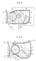
- the developer unit comprises a developer carrier 1′ which is rotatably supported and which is disposed in opposed relationship to a photosensitive member 10 with a gap g therebetween.
- a constraining member 3 ⁇ controls the thickness of a thin layer of developer T which is formed on the developer carrier 1′ and charges the developer T.
- a stirring paddle 5 for stirring developer T is disposed within a developer supply station.
- An anti-spill cover 6 prevents the developer T from spilling over the top of the developer carrier 1′.
- a developer vessel 7, defining the developer supply station, has the above described parts mounted thereon.
- a high voltage source E1 applies a developing bias to the developer carrier 1′.
- the developer carrier 1′ comprises a cylindrical metal shaft or metal support 1a having a coating of conductive resin layer 1b thereon.
- the shaft 1a may be formed of aluminium, stainless steel or the like, while the resin layer 1b may have a thickness of the order of 1.5 to 5mm and may be formed of a resin having conductive powder dispersed therein to exhibit a resistivity of the order of 104 to 1012 ohm-cm.
- the conductive powder may comprise conductive carbon, aluminium powder or silver powder, and the resin may comprise a thermosetting resin, such as a phenol, urea or melamine resin or a thermoplastic resin, such as polystyrene or acrylic resin.
- a coating of the conductive resin layer 1b on the metal shaft 1a is formed by initially providing a hollow-cylindrical member of conductive resin, to which the metal shaft 1a is bonded by using a conductive adhesive or in which the metal shaft 1a is positioned as a press fit.
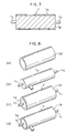
- a conductive resin which exhibits a resistivity of the order of 104 to 1012 ohm-cm and having a thickness of the order of 1.5 to 5 mm is initially formed into a hollow cylinder to provide a cylindrical member 1b′ of conductive resin.
- a metal shaft 1a carrying a pair of support stubs 1c at its opposite ends is polished to a high precision by a centred forced polishing operation.
- a conductive adhesive such as a silver filler containing epoxy adhesive or carbon filler containing acrylic adhesive, which has a resistivity equal to or less than 104 ohm-cm is applied to the surface of the metal shaft 1a as shown in Fig.8(c), and then the cylindrical member 1b′ is fitted over the metal shaft 1a. Finally, the centred forced polishing operation is again used to achieve a thickness of 1.5 to 5 mm for the conductive resin layer 1b and a tolerance of concentricity equal to or less than 10 ⁇ m for the outer diameter of the developer carrier 1′ as referenced to the outer diameter of the support stubs 1c located on the opposite ends of the metal shaft 1a.
- a developer carrier 1′ may be formed to an external diameter of 30 mm by utilising a stainless steel shaft 1a having a diameter of 24 mm which is then coated by a conductive resin layer 1b having a thickness of 3mm and having a resistivity of 105 ohm-cm which is obtained by dispersion of conductive carbon in phenol resin.
- the resulting developer carrier 1′ is driven at a peripheral speed of 100mm/sec, for example, in the direction shown by the arrow.
- a conductive resin layer 1b having a resitivity in a range of from 104 to 1012 ohm cm may be formed on the metal shaft 1a by coating the metal shaft 1a with polyurethane or polyester resin having a dispersion of conductive powder, such as conductive carbon, aluminium powder or silver powder so as to achieve a resistivity of the order of 104 to 1012 ohm cm.
- conductive powder such as conductive carbon, aluminium powder or silver powder
- the metal shaft 1a be eliminated completely, and a cylindrical member 1b′ formed on conductive resin having a resistivity of the order of 104 to 1012 ohm cm as a result of dispersion of conductive powder and which is free from flanges at its opposite sides may itself serve as a developer carrier.
- a voltage from the source E1 will not be uniform lengthwise of the developer carrier.
- the insufficient rigidity of the material may cause a flexure of the developer carrier, and in addition, it becomes difficult to maintain the circularity of the developer carrier which is directly related to an non-uniformity in the image density which is of paramount importance to the developer unit, thus presenting difficulties in their practical use.
- the developer carrier 1′ is located in the opening of the developer vessel 7 which contains an amount of developer T as a developer supply station, and the developer carrier 1′ is coated with the developer T by an applicator roller, not shown.
- the constraining member 3 ⁇ comprises a sheet of polyurethane rubber having a thickness of 3mm and a rubber hardness of 60°, for example, and is disposed in abutment with the developer carrier 1′.
- the developer T in the developer supply station within the vessel 7 will be conveyed to form a thin layer under the control of the constraining member 3 ⁇ to achieve a thickness of the order of 20 to 40 ⁇ m, and will be triboelectrically charged to the positive polarity by sliding contact with the developer carrier 1′ and the constraining member 3 ⁇ .
- the force which causes the adhesion of the developer T to the developer carrier 1′ will be electrostatic in nature in this instance.
- the thin layer of developer T which is formed on the developer carrier 1′ will be conveyed, as the developer carrier 1′ rotates, into the developing zone where it is in opposed relationship to the photosensitive member 10 rotating at the peripheral speed of 50mm/sec, for example, in the direction indicated by arrow, with a distance therebetween which is equal to gap g minus the thickness of layer of developer T.
- a resistivity in a range from 104 to 1012 ohm cm, preferably around 108 ohm cm, of the conductive resin layer 1b on the developer carrier 1′ yields a favourable development over a range of image varieties from a solid black to a halftone image whil suppressing and excessive transfer of developer T.
- the effect of any fluctuation in the output from the high voltage source E1 is diminished by the resistance which the conductive resin layer 1b on the developer carrier 1′ exhibits, reducing its influence upon the image quality.
- the developer T on the developer carrier 1′ which remains unused in the developing process will be recovered in the developer supply station within the vessel 7 through the anti-spill cover 6 as the developer carrier 1′ rotates. The described cycle is repeated to proceed with the developing process.
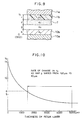
- the dielectric thickness f O can be determined from the following equation using a cross sectional arrangement of a dielectric layer model in the developing zone as shown in Fig. 9, which is formed by the photosensitive member 10 (photosensitive layer 10b and conductive substrate 10a), developer T, gap g and the developer carrier 1′.
- r, d, g and h are the thicknesses of the conductive resin layer 1b, the thin layer of developer T, the gap g and the photosensitive layer 10b, respectively
- ⁇ 2′ ⁇ 1′ ⁇ O and ⁇ s represent the dielectric constants of the conductive resin layer 1b, the layer of developer T, the gap g and the photosenstitive layer 10b respectively.
- the purpose of choosing a change of the gap g between 100 and 80 ⁇ m in the graphical illustration in Fig.10 is to consider a resulting change in the electric field E when the gap g varies due to mechanical accuracy of the developer carrier 1′.
- the rate of change in f0 is plotted against the thickness r of the conductive resin layer 1b in this graph over 0 to 5,000 ⁇ m to enable the influence of the thickness (including the presence and absence) of the conductive resin layer 1b to be recognised.
- Fig.10 which indicates the rate of change in the dielectric thickness f0 for a change in the gap g over varying thickness r of the conductive resin layer 1b
- the rate decreases with an increase in the thickness of the conductive resin layer 1b.
- the use of the conductive resin layer 1b on the developer carrier 1′ is effective to allow the accuracy which is required in machining the developer carrier 1′ to be alleviated as compared with the case wherein no conductive resin layer is used. Accordingly, a developer carrier 1′ having a conductive resin layer 1b is seen to be more suitable for its mass production while reducing the manufacturing cost.
- the developer carrier 1′ itself should achieve a tolerance of concentricity of its external diameter as referenced to the external diameter of the support stubs 1c located on the opposite ends of the metal shaft 1a which is equal to or less than 10 ⁇ m taking into consideration the accuracies of related parts and the assembly operation.
- a reduction in the absolute value of the dielectric thickness f0 which is caused by an increase in the thickness r of the conductive resin layer 1b causes a reduction in the strength of the electric field E, which can be accommodated for by controlling the developing bias Vb.
- Fig.10 shows that a decrease in the rate of change in the dielectric thickness f0 with an increase in the thickness of the conductive resin layer 1b is greatly reduced as the thickness further increases.
- an increased thickness of the conductive resin layer 1b causes difficulty in achieving accommodation by adjustment of the developing bias Vb. Accordingly, it is preferable for practical purposes that the thickness r of the conductive resin layer 1b is limited to or less than 5 mm. In addition, it is undesirable to use an increased thickness for the conductive resin layer 1b in order to suppress a dimensional change during the operation and storage.
- the conductive resin layer 1b is thin enough to be equal to or less than 1 mm, this is likely to cause a non-uniformity in the image density due to a non-uniform dispersion of conductive power within conductive resin layer 1b.
- the non-uniformity in the image density will also be caused by a non-uniformity in the thickness r of the conductive resin layer 1b, presenting practical problems.
- the developer carrier 1′ can act as a developing electrode to prevent any loss of the reproducibility of a solid black image.
- the rigidity of the developer carrier 1′ is sufficient to maintain the gap g between the developer carrier and the photosensitive member 10 to a high accuracy, enabling the development of an image which is free from non-uniformity in image density. Since the developer carrier 1′ comprises a coating of the conductive resin layer 1b around the metal shaft 1a, there resulted no potential distribution lengthwise of the developer carrier 1′, which would cause non-uniformity in the image density.
- the developer carrier 1′ Since the cylindrical member 1b′ of conductive resin is fitted over and secured to the peripheral surface of the metal shaft 1a, the developer carrier 1′, which is rendered incapable of producing non-uniformity in the image density by preventing a discharge of the developing bias, can be provided at a reduced cost and at a high accuracy by means of mass production.
- the sixth embodiment of developer unit shown in Fig.11 is a modification of that shown in Fig.1 in that the developer carrier 1′ used in the developer unit of the fifth embodiment (shown in Fig.7) is used in place of the developer carrier 1 and separate high voltage sources are used, including a high voltage source E2 associated with the porous member 2 and a high voltage source E3 associated with the constraining member 3.
- the source E3 is chosen to be of the same polarity as that to which the developer T is charged.
- the arrangement is similar to that shown in Fig.1, and accordingly corresponding parts are designated by like reference numerals or characters and will not be described in detail.
- the developer unit of the sixth embodiment operates substantially similarly to the developer unit of the first embodiment shown in Fig.1.
- the force which attracts the developer T to the developer carrier 1′ is an electrostatic force acting between the charge of the developer T and the conductive resin layer 1b on the developer carrier 1′.
- the constraining member 3 has been illustrated as a single member.
- the construction of the constraining member 3 is not limited thereto, and it may be constructed in different configurations as illustrated in Figs. 12(a), (b) and (c).
- the only requirement is that a portion of the constraining member 3 including a surface which abuts against the developer carrier 1′ exhibits a given resistivity and is adapted to allow the application of a high voltage thereto. Any separate member may be used to support such portion so as to enable the mechanical abutment of such portion against the developer carrier 1′, and still the assembly can function as the constraining member 3.
- the constraining member 3 comprises a conductive material 32 on the surface of a resilient member 31 which may be formed of urethane rubber.
- the conductive material 32 may be coated on the resilient material 31, but a bonding by means of an adhesive or a mechanical attachment is preferred in view of the useful life and the stability.
- the constraining member 3 comprises a block of conductive material 34 secured to the free end of a resilient metal plate 33 which may be formed of phosphor bronze or spring steel.
- the constraining member 3 comprises a conductive material 37 applied to the surface of a resilient member 36 which is in turn secured to a resilient metal plate 35 which may be formed of phosphor bronze or spring steel.
- the porous member 2 used in the sixth embodiment shown in Fig.11 is replaced by the fibrous conductive member 8 used in the second embodiment shown in Fig.3.
- the arrangement is similar to that of the sixth embodiment, and accordingly, corresponding parts are designated by like reference numerals and characters and will not be described in detail. Again, this embodiment operates in the similar manner as the sixth embodiment shown in Fig.11.
- the constraining member 3 is disposed at the top of the developer carrier 1′ while the anti-spill cover 6 is disposed alongside the bottom of the developer carrier 1′.
- a partition 9 is disposed on top of and above the porous conductive resilient member 2 disposed within the developer vessel 7 for preventing the developer T distributed around the stirring paddle 5 from moving directly to the developer carrier 1′ without being previously engaged by the porous member 2.
- the partition 9 is effective to introduce such portion of the developer T, which has been blocked from being conveyed into the developing zone as the constraining member 3 defines a thin layer, as well as that portion of the developer T which is scraped off the developer carrier 1′ which remained after the development, into the developer vessel 7 to the region of the stirring paddle 5.
- the partition 9 may be formed of a resin, for example, but is preferably formed of a metal which is then connected to the electrical earth in consideration of the charge of the developer T and the subsequent charged condition of the developer T. If placed in contact with the porous conductive resilient member 2, the partition 9 cannot cause a leakage of a high voltage from the source E2 because of the resistivity of the porous member 2 which is of the order of 103 to 106 ohm-cm.
- the developer unit of the eighth embodiment operates in substantially the same manner as the developer unit of the sixth embodiment shown in Fig.11.
- the porous member 2 it is possible to replace the porous member 2 by the fibrous conductive member 8 as used in the seventh embodiment shown in Fig.13.
- the direction of rotation shown for the porous member 2 is exemplary only, and it may rotate in the opposite direction.
- the presence of the partition 9 is also preferred in this instance.
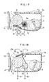
- the conductive constraining member 3′ is formed as a lamination of a non-conductive portion 3a and a conductive portion 3b, and the high voltage source E2 connected to the porous member 2 is separate from the high voltage source E3 which is connected to the conductive portion 3b of the constraining member 3′.
- the arrangement is similar to that of the first embodiment shown in Fig.1 and accordingly, corresponding parts are designated by like reference numerals and characters and will not be described specifically.
- the purpose of replacing the conductive constraining member 3 by the laminate 3′ is to improve the useful life and the reliability of the resulting developer unit. Specifically, if a constraining member 3 is formed by a dispersion of conductive material therein or containing a conductive material deposited on or coated on the surface thereof and disposed for contact with the developer carrier 1 which carries the developer thereon, mechanical abrasion of the surface of the constraining member 3 which is placed in contact with the developer carrier 1, is caused, in particular, when the surface of the developer carrier 1 is roughened. Where the constraining member 3 is formed by dispersion, there results a differential abrasion between the resin which represents a dispersion medium and the conductive material which represents a dispersed phase.
- the deposited or coated layer may be abraded or may become exfoliated.
- the stability of the charging and the formation of the thin layer will both depend on the quality of the constraining member 3, resulting in a degraded reliability and a reduced life of the developer unit.
- the non-conductive portion 3a of the constraining member 3′ is formed by a sheet of silicone rubber or urethane having a thickness of the order of 2 to 3 mm and hardness of the order of 60° to 80°, and the conductive portion 3b is applied to the opposite side thereof away from the side thereof which is disposed for abutment against the developer carrier 1.
- the conductive portion 3b may be formed in a number of ways, including a coating of conductive material, such as conductive carbon or metal filler on a resilient material which forms the non-conductive portion 3a, or bonding a thin film of a metal, such as copper, aluminium or stainless steel, to such resilient material by using a conductive adhesive, such as a silver filler containing epoxy adhesive or carbon filler containing acrylic adhesive or evaportion of aluminium thereon.
- a conductive adhesive such as a silver filler containing epoxy adhesive or carbon filler containing acrylic adhesive or evaportion of aluminium thereon.
- the non-conductive portion 3a On the side disposed for abutment with the developer carrier 1, the non-conductive portion 3a exhibits a resistivity equal to or greater than 1013 ohm-cm, and such insulating material is effective to prevent a leakage between the source E3 connected to the conductive portion 3b of the constraining member 3′ and the source E1 connected to the developer carrier 1, thus allowing the constraining member 3′ and the developer holder 1 to be maintained at their respective high potentials.
- the developer T which is charged by the porous member 2 will be formed into a thin layer on the developer carrier 1 under the control of the constraining member 3′ so as to have a thickness of the order of 20 to 40 ⁇ m.
- the non-conductive portion 3a of the constraining member 3′ is insulating, it has a dielectric constant, so that, when a high voltage is applied to the conductive portion 3b of the constraining member 3′ which is connected to the source E2, an induced charge will be developed on the side of the non-conductive portion 3a which is disposed for abutment against the developer carrier 1, causing a charging by contact charging or triboelectric charging.
- the entire constraining member 3′ is formed as a laminate construction, but the construction of the constraining member 3′ is not limited thereto, but may assume different configurations as indicated in Figs. 16(a), (b), (c) and (d).
- the side of the constraining member 3′ which is disposed for abutment with the developer carrier 1 is formed as a non-conductive portion 3a while the opposite side is formed with the conductive portion 3b, the requirement for a mechanical abutment against the developer carrier 1 is satisfied.
- the constraining member 3′ comprises an insulating resin layer 39 applied to a resilient plate 38 which may be formed of a metal, such as phosphor bronze or spring steel.
- the constraining member 3′ comprises a similar resilient metal plate 40, to the free end of which is secured a block of resilient material 41 having a conductive material 42 formed on its surface.
- the constraining member 3′ comprises a block of resilient conductive member 43 which may be formed by a sheet of silicone rubber or the like, having conductive material dispersed therein, and a portion of which, disposed for abutment with the developer carrier 1, is replaced by a block 44 of insulating material which may be formed of silicone rubber which does not have a dispersion of conductive material therein.
- the constraining member 3′ comprises a so-called graded function material 45 which is formed by a metal sheet as may be formed by chromium dioxide (CrO2) on which a ceramic layer is grown as a crystal, with a high voltage being applied to the metal surface.
- graded function material 45 is formed by a metal sheet as may be formed by chromium dioxide (CrO2) on which a ceramic layer is grown as a crystal, with a high voltage being applied to the metal surface.
- the porous member 2 is replaced by the fibrous conductive member 8.
- the arrangement is similar to that of the ninth embodiment shown in Fig.15, and accordingly corresponding parts are designated by like reference numerals or characters and will not be described specifically.
- This developer unit operates in substantially the same manner as the developer unit of the ninth embodiment shown in Fig.15.
- the constraining member 3′ is disposed at the top of the developer carrier 1 while the anti-spill cover 6 is disposed at the bottom thereof.
- a partition 9 similar to that used in the eighth embodiment shown in Fig.14 is disposed on top of and above the porous member 2 located within the developer vessel 7.
- the developer unit of the eleventh embodiment operates substantially similar as the developer unit of the ninth embodiment shown in Fig.15.
- the direction of rotation shown in this Figure of the porous member 2 is exemplary, and it may rotate in the opposite direction. In this instance, it is preferred that the partition 9 be provided.
- the constraining member 3 is a composite of a resilient metal plate 33 and a conductive material 34 as shown in Fig.12(b).
- the arrangement is similar to that of the first embodiment shown in Fig.1, and accordingly, corresponding parts are designated by like reference numerals or characters and will not be specifically described.
- the developer unit of this embodiment operates substantially similarly as the developer unit of the first embodiment shown in Fig.1.
- the composite constraining member 3 may be replaced by a different composite constraining member 3 as shown in Fig.12(a) or (c). The operation remains unchanged.
- the composite constraining member 3 may be disposed at the top of the developer carrier 1 while the spill cover 6 may be disposed along the bottom thereof.
- the porous member 2 may be replaced by the fibrous conductive member 8.
- the developer carrier 1 of the first embodiment shown in Fig.1 is replaced by the developer carrier 1′ (see Fig.7) of the fifth embodiment shown in Fig.6, and the conductive constraining member 3 of the first embodiment is replaced by a constraining member 3′ comprising a laminate comprising a non-conductive portion 3a and a conductive portion 3b.
- a high voltage source E2 which applies a high voltage to the porous member 2 is separate from a high voltage source E3 which applies a high voltage to the conductive portion 3b of the constraining member 3.
- the arrangement is similar to that of the first embodiment shown in Fig.1, and accordingly, corresponding parts are designated by like reference numerals or characcters as used in Fig.1 and will not be specifically described.
- the developer unit of the thirteenth embodiment operates substantially similarly as the developer unit of the first embodiment shown in Fig.1, but, when the developer T is charged, it is supplied with charge from the porous member 2 so as to be electrostatically held attracted to the developer carrier 1′ and is charged in a stable manner by the induced charge which is developed at the non-conductive portion 3a of the constraining member 3 before it is conveyed into the developing zone.
- the side of the constraining member 3′ which is disposed for abutment with the developer carrier 1′ comprises the non-conductive portion 3a while the opposite side comprises the conductive portion 3b so that the charging and the formation of the thin layer of the developer T take place in a stable and reliable manner, assuring a stable and reliable image reproduction by the developer carrier 1′ which carries the conductive resin layer 1b.
- the constraining member 3′ may comprise a composite as shown in Figs. 16(a) to (d), and in addition, the constraining member 3′ may be disposed at the top of the developer holder 1′ while the anti-spill cover 6 may be disposed alongisde the bottom thereof as shown in Fig.5.
- the porous member 2 of the thirteenth embodiment shown in Fig.20 is replaced by the fibrous conductive member 8.
- the arrangement is similar to that of the thirteenth embodiment shown in Fig.20, and accordingly, corresponding parts are designated by like reference numerals or characters and will not be described in detail.
- the developer unit of the fourteenth embodiment operates in substantially the same manner as the developer unit of the thirteenth embodiment shown in Fig.20.
- the developer unit uses a developer T which is charged to a positive polarity, but the invention is equally applicable to developer units wherein the developer T is charged to a negative polarity.
Landscapes
- Physics & Mathematics (AREA)
- General Physics & Mathematics (AREA)
- Dry Development In Electrophotography (AREA)
Abstract
Description
- The invention relates to developer units, and in particular, to developer units utilising a non-magnetic single component developer. The invention also relates to the manufacture of developer carriers for developer units.
- Prior art techniques to develop an electrostatic latent image which may be formed by an exposure of a uniformly charged photosensitive member in accordance with image information generally include a two component developer process which uses a toner and a carrier, in particular such a process utilising a magnetic brush, which will be hereafter referred to as a two component magnetic brush developing process. However this process suffers from practical difficulties including an increased size of the resulting developer unit, difficulty in achieving a stable mixture ratio of toner and carrier and an associated difficulty in charging the toner.
- Recently, a magnetic brush developing process utilising a single component developer in which the toner itself exhibits a magnetic property, hereafter referred to as a single component magnetic brush developing process, has been available on the market. However, while it achieves a reduction in the size of the resulting developer unit, the single component magnetic brush process presents difficulties in achieving a colour image in view of the fact that the developing powder includes a magnetic powder.
- In view of the foregoing, there is proposed a developing process utilising a non-magnetic, single component developer (hereafter referred to as a non-magnetic single component developing process), which is still under investigation. This process is again categorised into a process in which the development takes place by the contact between a developer and an electrostatic latent image carrier such as a photosensitive member, for example, and another process in which the developer and the latent image carrier are maintained out of contact from each other while the development takes place by causing the developer to fly onto the carrier.
- The former or contact process results in excellent results in improving the image density and the ease of supplying a developer, but suffers from susceptibility to the occurrence of a background fogging which is caused by the contact betweeen the developer and the latent image carrier. In addition, it exhibits the disadvantage that it cannot be adopted in a single drum, multiple colour, single transfer process which is intended to achieve a simplification of an overall developer unit and a reduction in the cost in producing a colour image, in view of the contacting nature of the process which gives rise to the problem of colour mixture. Accordingly, resort must be had to the latter or non-contact, flying developing process which utilises the non-magnetic single component developer.
- In a conventional developer unit which utilises the non-contact, flying developing process, the use of the non-magnetic single component developer may cause a poor image, such as a thinning or braking of the image, unless a supply of developer to the holder, its charging, the formation of a thin layer thereof, conveyance to a developing zone and the flying capability are properly controlled together with a satisfactory achievement of the removal, stirring action and circulation of the developer.
- Considering, for example, a conventional developer unit in which a developer is charged and a thin layer is formed simultaneously by means of a constraining member, such as a pressure blade, the degree to which the developer is charged cannot be stabilised in view of the triboelectric nature of charging, but undergoes a large variation subject to the material and a change in the surface condition of the constraining member, resulting in poor reliability. In addition, residual developer which remains on the carrier after for developing step cannot be removed from the carrier, and is allowed to be used again in the next following developing step as the carrier rotates. In this manner, difficulties are experienced in achieving a stable charging of the developer and a satisfactory stirring action of the developer.
- In a conventional developer unit which utilises the non-contact, flying, non-magnetic single component developing process, it has been known to apply a developing bias, such as an electric pulse of a a.c. bias, to the developer carrier in order to prevent a non-image area in the latent image from being developed, to impart a proper amount of edge effect to the image or to improve the tone quality. However, a gap g between the developer carrier and the electrostatic latent image carrier must be maintained very small; of the order of 0.5 to 0.02 mm. If a metal developer carrier is used which is made of a commonly used metal, such as aluminium, stainless steel or the like, the choice of a high developing bias which is applied to the developer carrier from a high voltage source will cause the liability of the developing bias to discharge, which upon occurrence, reduces the potential of the developer carrier to a point near earth potential, with the consequence that a resulting low bias phenomenon occurs across the entire developer carrier to produce a black traversing pattern running across the background (non-image area) of a copy or the electric breakdown of the air will produce a white dot discharge pattern in the image area, thus causing a degradation in the image quality. On the other hand, the choice of a low developing bias cannot assure a satisfactory developing capability. These difficulties can be overcome by the use of an insulating developer carrier, but this results in the loss of the developing electrode effect, degrading the reproducibility of a solid black image.
- To accommodate for this, there has been proposed a developer unit using a developer carrier which comprises a cylindrical member formed by a conductive resin in which a conductive powder is dispersed and having openings at its opposite ends, to which a pair of end supports carrying stub shafts are coupled, with the resistivity of the conductive resin forming the cylindrical member chosen to be in a range from 10⁴ to 10¹² ohms cm with a wall thickness in a range from 0.5 to 3 mm (see, for example JP-A-85/80875. In the developer unit using such a developer carrier, the resistivity of the conductive resin suppresses the discharge of the developing bias, and thus the choice of a high applied developing bias cannot result in the appearance of a black traversing pattern in the background (or non-image area) of a copy which might have been otherwise caused by the discharge of the developing bias. In addition, the occurrence of a discharge pattern in the form of white dots in the image area is also avoided, and the reproducibility of a solid black image is not degraded.
- However, in this developer unit, the construction of the developer carrier which is formed of a conductive resin and which is supported at its opposite ends by the pair of stub supports present difficulty in ensuring the rigidity of the developer carrier and the concentricity of the outer diameter thereof with respect to the axis. This in turn presents difficulty in maintaining a gap between the developer carrier and the latent image carrier to a high accuracy. Any variation in the gap is reflected in non-uniformity of the image density. When the developer carrier has an outer diameter less that 30 mm or a length greater than 200 mm, sufficient rigidity cannot be ensured, causing a flexure therein. In addition, error in the concentricity of the outer diameter with respect to the axis will exceed 10 µm, causing a significant non-uniformity in the image density, which prevented its practical use. In addition, when a developing bias is applied to the cylindrical member, there will be produced a potential distribution lengthwise of the developer carrier, which also contributes to increasing the non-uniformity in the image density.
- It is an object of the invention to provide a developer unit utilising a non-magnetic single component developer in which the functions of controlling the supply, the charging, the formation of a thin layer of, the conveyance to a developing zone and the flying capability of a developer as well as the removal, stirring action and circulation of the developer are separated, and in which the charging of the developer which has been performed in the past only through the triboelectric charging operation is achieved by a positive charge injection operation by the use of a porous conductive resilient member or fibrous conductive member in combination with a constraining member to which a voltage is applied so that the developer is charged in a stable manner while improving the stirring action upon the developer to enable a stabilised developing operation which is free from any defect in the image quality.
- It is another object of the invention to provide a developer unit which permits a voltage applied to a developer carrier, a porous conductive resilient member or fibrous conductive member and a constraining member to be controlled to enable a proper setting of developing conditions or parameters, thereby enabling control to be exercised over the image density in the event of any variation in the environment, in the quality of the developer or the electrical resistance of component members or a variation from batch to batch.
- A developer unit according to the invention, in which a non-magnetic single-component developer is supplied to the surface of a developer carrier and is formed into a substantially uniform thin layer thereon by means of a constraining member and in which an electrical developing bias is applied to the developer carrier to cause developer to fly across a gap onto an image area of an electrostatic latent image formed on a latent image carrier opposed to the developer carrier, is characterised in that the developer carrier is metallic or comprises a metal core and an electrically conductive yieldable charging member is rotatably disposed in physical contact with the developer carrier, and in that the constraining member is electrically conductive and a high voltage is applied to the charging member and the constraining member as well as the developer carrier, whereby the constraining member charges the developer on the developer holder to a predetermined potential.
- It is a further object of the invention to provide a developer unit which uses a developer carrier carrying a conductive resin layer on its surface to prevent occurrence of a discharge of a developing bias thereby to enable a developing operation to be performed in a manner which avoids any defect in the image quality while allowing an image, free from a density non-uniformity, to be developed.
- It is an additional object of the invention to provide a process of manufacturing a developer carrier in a facilitated manner and to a high accuracy, the carrier preventing the occurrence of a discharge of a developing bias to enable an image, free from non-uniformity in density to be developed.
- The invention includes a developer unit whose developer carrier comprises a metal case and a conducting resin layer on the core. The layer preferably has a thickness from 1.5 to 5mm and a resistivity from 10⁴ to 10⁸ ohm-cm.
- The invention also includes a process of manufacturing a developer carrier comprising the steps of
shaping a cylindrical member of conductive resin;
polishing a cylindrical metal core;
fitting the cylindrical member over the metal core and securing it to the metal core;
and polishing the cylindrical member as secured to the metal core. - According to the invention, the control over the supply, the charging, the formation of a thin layer of, the conveyance to a developing zone and a flying capability of a developer as well as the removal, stirring action and circulation of the developer, which form essential steps in a developing process which utilises a non-magnetic single component developer, are functionally separate from each other. This eliminates any instability in the developing conditions which may be caused by the triboelectric charging or a failure to take a flow condition of the developer into consideration. A developing electrode effect which is imparted to the developer carrier can be advantageously established for a wide range of image varieties including a solid black image to a halftone image. Suitable developing conditions may be established which are adapted to the production of thin lines, in particular. In this manner, the reliability of the developing process can be improved by achieving a stabilised image quality. In addition, the invention exhibits a stabilised characteristic against environment by the use of a charge injection technique rather than the triboelectric charging technique which is greatly influenced by the environment factors or the surface condition of the material.
- The developer unit is internally constructed such that the porous conductive resilient member or fibrous conductive member is effective to feed the developer, so that, in the event foreign matter is present in admixture, it is only allowed to reach the top portion of such conductive member, but is prevented from proceeding into the following step, thus assuring an enhanced reliability in this respect.
- The developer carrier may comprise a metal carrier or core which is coated by a conductive resin layer. This reduces a change upon the image quality when a developing bias is applied to the developer carrier and allows a fog-free and sharply defined image to be obtained. The likelihood of discharge is eliminated if a high voltage is applied as a developing bias. In addition, a high precision can be mechanically maintained for a developer carrier of a reduced diameter and increased length.
- A cylindrical member of conductive resin is fitted over and secured to the surface of the metal carrier, allowing the developer carrier to be produced with a high accuracy and at a low cost through mass production. The resulting developer carrier is effective to prevent discharge from the developing bias and to produce an image which is free from a non-uniformity in the image density.
- The invention is further described, by way of example, with reference to the accompanying drawings, in which:-
- Fig.1 is a schematic cross section of a developer unit according to a first embodiment of the invention;
- Fig.2 is a sectional view, to a larger scale, of part of the developer unit shown in Fig.1, illustrating flow of the developer;
- Fig.3 is a cross-section of a developer unit according to a second embodiment of the invention;
- Fig.4 is a cross-section of a developer unit according to a third embodiment of the invention;
- Fig.5 is a cross-section of a developer unit according to a fourth embodiment of the invention;
- Fig.6 is a cross-section of a developer unit according to a fifth embodiment of the invention;
- Fig.7 is a longitudinal section, illustrating a developer carrier shown in Fig.6 to a larger scaler;
- Fig.8 is a series of perspective views illustrating steps used to manufacture the developer carrier shown n Fig.7;
- Fig.9 is a schematic illustration of dielectric layers used in the developing zone of the developer unit of the fifth embodiment shown in Fig.6;
- Fig.10 graphically shows the rate of change in the thickness of a dielectric layer as a gap changes in the dielectric layer model shown in Fig.9;
- Fig.11 is a cross-section of a developer unit according to a sixth embodiment of the invention;
- Fig.12 is a series of cross-sections illustrating a sequential deformation of the constraining member shown in Fig.11;
- Fig.13 is a cross-section of a developer unit according to a seventh embodiment of the invention;
- Fig.14 is a cross-section of a developer unit according to an eighth embodiment of the invention;
- Fig.15 is a cross-section of a developer unit according to a ninth embodiment of the invention;
- Fig.16 is a series of cross-sections illustrating a sequential deformation of the constraining member shown in Fig.15;
- Fig.17 is a cross-section of a developer unit according to a tenth embodiment of the invention;
- Fig.18 is a cross-section of a developer unit according to an eleventh embodiment of the invention;
- Fig.19 is a cross-section of a developer unit according to a twelfth embodiment of the invention;
- Fig.20 is a cross-section of a developer unit according to a thirteenth embodiment of the invention; and
- Fig.21 is a cross-section of a developer unit according to a fourteenth embodiment of the invention.
- A developer unit according to the first embodiment of Fig.1 comprises a developer support or
carrier 1 which is rotatably supported in opposed relationship to a photosensitive member (electrostatic latent image carrier) 10 on which an electrostatic latent image is formed, with a gap g between thedeveloper carrier 1 and theimage carrier 10. A porous conductiveresilient member 2 is rotatably mounted and partly maintained in contact with thedeveloper carrier 1. A conductive constrainingmember 3 controls the thickness of a layer of non-magnetic single component developer T to form a thin layer of developer T on thedeveloper carrier 1 and charges the developer T to a given potential. A stirringpaddle 5 for stirring the developer T is contained in a developer supply station. Ananti-spill cover 6 prevents the developer T from spilling over the top of thedeveloper carrier 1. The members mentioned above are mounted on adeveloper vessel 7 which defines the developer supply station. A high voltage source E1 is connected to thedeveloper carrier 1, and another high voltage source E2 is connected to theporous member 2 and to the constrainingmember 3. - The
developer carrier 1 comprises a shaft of a metal, such as aluminium or stainless steel. - The porous conductive
resilient member 2 comprises a roller or a material, such as soft polyurethane foam, having a three-dimensional skeleton structure and containing conductive carbon and formed on ametal shaft 2a which is supported in a rotatable manner by the sidewalls of thedeveloper vessel 7. Theporous member 2 is bonded to themetal shaft 2a by utilising an electrically conductive adhesive, such as an epoxy adhesive containing silver (Au) filler or an acrylic adhesive containing carbon filler. Theporous member 2 has a resistivity of the order of 10³ to 10⁶ ohm-cm and hence there can be no leakage between the high voltage source E2 to which theporous member 2 is connected and the high voltage source E1 to which thedeveloper carrier 1 is connected, allowing high potentials to be maintained independently on theporous member 2 and thedeveloper carrier 1. The developer T is charged to the same polarity as the polarity of the high voltage source E2. Theporous member 2 has a porosity level, which may be from 15 to 45 pores or cells per 25 mm. It is found that theporous member 2 preferably has a contact depth (or depth of engagement) with respect to thedeveloper carrier 1 of the order of 0.5 to 1.0 mm in consideration of the efficiency of conveying the developer T and the removal of the developer T which may remain on thedeveloper carrier 1 subsequent to the developing process. - The constraining
member 3 is formed of a silicone rubber sheet having a hardness from 60° to 80° and which is made electrically conductive by a dispersion or attachment of conductive material (for example, conductive carbon), the member having a thickness of the order of 2 to 3 mm. The constrainingmember 3 abuts against thedeveloper carrier 1 by its body portion or by both its body and edge portions, and is effective to control the thickness of a layer of the developer T formed on thedeveloper carrier 1 so that the thickness may be of the order of 20 to 40 µm while charging the developer T to a given potential. The constrainingmember 3 has a resistivity of the order of 10³ to 10¹⁰ ohm-cm, and accordingly there occurs no leakage between the high voltage source E2 to which the constrainingmember 3 is connected and the high voltage source E1 to which thedeveloper carrier 1 is connected, allowing given high potentials to be maintained independently on the constrainingmember 3 and on thedeveloper carrier 1. - The stirring
paddle 5 is not limited to any particular configuration, but preferably is shaped to achieve an effective stirring action and circulation of the developer T in the developer supply station defined within thedeveloper vessel 7 without forming any stagnation or build-up of the developer T therein. -
anti-spill cover 6 is suitably formed of a urethane rubber sheet having a thickness of the order of 0.02 mm thick. - The
developer carrier 1, theporous member 2 and the stirringpaddle 5 are connected together through gears (not shown) outside thedeveloper vessel 7, and are driven for simultaneous rotation in directions indicated by arrows as the developing process is started. - In operation, as the developing process is started, the developer carrier, the
porous member 2 and the stirringpaddle 5 begin to be driven to rotate in respective directions indicated. A quantity of the developer T which is contained in the developer supply station defined within thedeveloper vessel 7 tends to be conveyed, as indicated by an arrow a in Fig.2, by the rotation of theporous member 2 into an area of contact between theporous member 2 and thedeveloper carrier 1 where the developer T is charged by theporous member 2 which is connected to the high voltage source E2. - The charged developer T moves in a manner indicated by arrows b shown in Fig.2 as both the
developer carrier 1 and theporous member 2 rotate. Specifically, part of the charged developer T is conveyed to form a thin layer on thedeveloper carrier 1 while being controlled by the constrainingmember 3 to a thickness of the order of 20 to 40 µm and is charged to a given potential by the constrainingmember 3. The force which attracts the developer T to thedeveloper carrier 1 is a mirror image force acting between the charge of the developer T and thedeveloper carrier 1. - A thin layer of the developer T which is formed on the
developer carrier 1 is conveyed to a developing zone as thedeveloper carrier 1 rotates in order to develop an electrostatic latent image formed on thephotosensitive member 10. When so conveyed, it will be located opposite to thephotosensitive member 10 at a distance therefrom (which is equal to the gap g minus the thickness of the layer of developer T). - The
developer carrier 1 is connected to a high voltage source E1. Because, in the developing zone, a surface charge density in an image area of the electrostatic latent image formed on the photo-sensitive member 10 is different from a corresponding density in a non-image area of the latent image, the electrostatic force of attraction F = qE (where q represents the charge of developer T and E represents the electric field in the developing zone) will be different between the image area and the non-image area. As a consequence, the developer T will fly off thedeveloper carrier 1 and towards thephotosensitive member 10 for purpose of developing, only in the region of the image area. - A choice of peripheral speed of the
developer carrier 1 which is greater than that of thephotosensitive member 10 is an effective technique to assure image density. - An amount of developer T which remains on the
developer carrier 1 without being utilised in the developing process will be conveyed towards theanti-spill cover 6 as thedeveloper carrier 1 rotates further so as to be received again within the developer supply station defined within thedeveloper vessel 7. Theanti-spill cover 6 is disposed in abutment with thedeveloper carrier 1, but such abutment takes place at a curved portion of thecover 6 which is held in gentle contact with thedeveloper carrier 1, and accordingly the developer T will be allowed to move into thevessel 7 without being scraped off thedeveloper carrier 1 by thecover 6. - The developer T which remains on the
developer carrier 1 and which is conveyed into thedeveloper vessel 7 will be conveyed towards the porous conductiveresilient member 2, as indicated by an arrow c. The latter member is effective to scrape the remaining developer from thedeveloper carrier 1, allowing the scraped developer to be conveyed towards the stirringpaddle 5 disposed within thevessel 7, in the manner indicated by an arrow b in Fig.2, as theporous member 2 rotates. The developer T will then be again stirred and circulated through thevessel 7 for repeated contribution to the developing process. - The choice of a peripheral speed of the
porous member 2 greater than that of thedeveloper carrier 1 is effective to improve the scraping effect upon the developer T which remains on thedeveloper carrier 1, and also contributes to the action of theporous member 2 which supplies the developer T to thedeveloper carrier 1 and charges it in preparation to the next following developing cycle. The described operation is repeated to run a developing process. - As the developer T is consumed, a fresh quantity thereof must be replenished to the developer supply station within the
developer vessel 7. This may take place by opening afeed lid 7a or by utilising a cartridge. - In the developer supply station within the
developer vessel 7, residual developer T and fresh developer T will be in admixture. However, since it is only that portion of the developer T subject to contact and a conveying action of theporous member 2 and the constrainingmember 3 which contributes to the deposition of the developer T upon thephotosensitive member 10, the degree of charging can be controlled by such member, achieving a stabilised degree of charging irrespective of the history of the developer T. This in turn stabilises the force F = qE with which the developer T flies onto the image area during the developing process, thus achieving a stabilised image quality. - While the high voltage source E2 is shown as a d.c. source, it is also effective to utilise a superposed d.c. and a.c. source to prevent the agglomeration of the developer T while improving its conveying capability. However, if the a.c. is used in superposition, the source still requires a d.c. component to prevent the polarity of the developer T from changing.
- In the second embodiment of Fig.3, the
porous member 2 used in Fig.1 is replaced by a fibrousconductive member 8. In other respects, the arrangement is similar to that of the first embodiment shown in Fig.1 and accordingly, corresponding parts are designated by reference numerals or characters, and the repeated description will be omitted. - Specifically, the fibrous
conductive member 8 is in the form of a brush comprising either a conductive resin fibre, such as nylon or rayon, in which a conductive carbon is dispersed, or a conductive resin fibre, such as nylon or rayon, having a core of conductive material. The fibre may be made conductive by a post-processing step such as depositing fine particles of conductive carbon to the surface thereof. The thickness of the conductive resin fibre may be 100 to 2,000 denier/100 fibres, or each fibre may be of the order of 1 to 20 denier where one denier corresponds to the thickness of a fibre when one gram of the material extends to a length of 9,000 m. A suitable density will be of the order of 15.5 to 1550 fibres per sq.mm (10 to 1,00 x 10³ fibres per inch square). - The fibrous
conductive member 8 is formed as a brush mounted on ametal shaft 8a which is rotatably supported by the sidewalls of thedeveloper vessel 7, in a similar manner to theporous member 2. The fibrousconductive member 8 may be bonded to themetal shaft 8a by utilising a conductive adhesive, such as silver (Au) filler containing epoxy adhesive or carbon filler containing acrylic adhesive, as is the case with theporous member 2. - The intended purpose of the fibrous
conductive member 8 may be served by choosing a depth of contact between the fibrousconductive member 8 and thedeveloper holder 1 of the order of 0.5 to 2.0 mm. - The number of revolutions per minute of the fibrous
conductive member 8 depends on its diameter, but its peripheral speed is chosen to be equal to or greater than that of thedeveloper carrier 1 in contrast with the case of theporous member 2 of Fig.1. - The developer unit of the second embodiment operates in a similar manner to that shown in Fig.1, and therefore will not be described.
- In the third embodiment of Fig.4, the
developer carrier 1 is provided by forming adielectric layer 11 on the surface of a metal shaft which supports thedeveloper carrier 1 and remains the same as in Fig.1. In other respects, parts shown in Fig.4 are similar to those shown in Fig.1, and accordingly are designated by like numerals and characters. - The
dielectric layer 11 may be formed of a polymer material, such as polyester, polyethylene, polyvinylidene fluoride, polypropylene or the like, and desirably has a thickness of the order of 50 to 100 µm. By providing a dielectric material in the form of electret, it may be rendered effective to prevent the developer T sputtering in addition to serving for conveyance of the developer T and development. - The developer unit of the third embodiment operates substantially in a similar manner to the developer unit of the first embodiment shown in Fig.1, but the presence of the
dielectric layer 11 results in a different nature of force acting upon the developer T. Specifically, the developer T which is conveyed by theporous member 2 upon initiation of the developing process will be held attracted to thedeveloper carrier 1 as a result of its charging thedielectric layer 11 on thedeveloper carrier 1 together with theporous member 2 connected to the high voltage source E2 and the constrainingmember 3 as the developer T itself is charged by themembers dielectric layer 11 is in effect charged by the charged developer T, and accordingly the force of attraction, acting upon the developer T towards thedeveloper carrier 1 will be an electrostatic force, rather than a mirror image force which was effective in the developer unit of the first embodiment. - The electric resistance of the
porous member 2, the constrainingmember 3 and thedielectric layer 11 as well as the potential of the high voltage source E2 are chosen so that the potential of theporous member 2 and the constrainingmember 3 near their surfaces is greater in absolute magnitude than the surface potential of thedielectric layer 11. - In the developer unit of the third embodiment, the relationship between the various potentials should be such that
- |the potential of image area of electrostatic latent image | < |the potential of developer carrier | < |the surface potentials of porous member and constraining member|
- |the potential of developer carrier | < |the surface potentials of porous member and the constraining member| ≦ |the potential of image area of electrostatic latent image|
- While the residual developer T on the
developer carrier 1 and to be removed therefrom, is subject to the action of theporous member 2, the surface potential of thedielectric layer 11 remains unchanged, which is effective to achieve a more stabilised deposition of the developer T upon thedeveloper carrier 1 in the next following developing process. - The developer unit of the third embodiment may require at least one revolution of the
developer carrier 1 to charge thedielectric layer 11 before the developing step can take place, but this presents no problem. - In the developer unit of the third embodiment, it is also advantageous for the purpose of assuring a favourable supply of the developer T to choose a peripheral speed of the
porous member 2 which is equal to or greater than that of thedeveloper carrier 1, as in the first embodiment shown in Fig.1. - It is to be noted that in the developer unit of the third embodiment, the porous conductive
resilient member 2 may be replaced by the fibrousconductive member 8 shown in Fig.3. - In the developer unit of the fourth embodiment of Fig.5, the direction of rotation of the
developer carrier 1 is opposite to that shown for the first embodiment shown in Fig.1. Accordingly, because corresponding parts are similar to those used in the first embodiment shown in Fig.1, they are designated by like numerals and will not be described in detail. - However, in the developer unit of the fourth embodiment, the constraining
member 3 is disposed at the top of thedeveloper carrier 1 while theanti-spill cover 6 is disposed adjacent to the bottom of thedeveloper carrier 1. - The operation of the developer unit of the fourth embodiment remains substantially similar to that of the developer unit of the first embodiment shown in Fig.1.
- The
developer carrier 1, the porous conductiveresilient member 2 and the stirringpaddle 5 rotate in directions indicated by arrows in Fig.5, and the developer T is conveyed towards thedeveloper carrier 1 as theporous member 2 rotates. As it is being conveyed, the developer T is charged by the porous conductiveresilient member 2 which is connected to the high voltage source E2 and, as it is charged, it is held attracted to thedeveloper carrier 1 by the mirror image force for its subsequent conveyance by the rotation of thedeveloper carrier 1. - the constraining
member 3 forms a thin layer of developer, of the order of 20 to 40 µm and also charges the developer T to a given stable potential so that it is conveyed into the developing zone as thedeveloper carrier 1 rotates. In the developing zone, the developer T is used to develop an electrostatic latent image formed on thephotosensitive member 10 according to the relative force relationship as mentioned above in connection with previous embodiments, and residual developer T which was not utilised in the developing step will move past theanti-spill cover 6 as thedeveloper carrier 1 rotates to be removed therefrom by theporous member 2. Subsequently, the developer T is subjected to a stirring and circulating action within thedeveloper vessel 7 by the stirringpaddle 5 located within the developer supply station for its use in subsequent development process. - The direction of rotation of the
porous member 2 shown in Fig.5 is an example, but the direction of rotation may be the opposite to accommodate for a reduced amount of developer T within the developer supply station. - It is also possible to provide a
dielectric layer 11 on the surface of thedeveloper carrier 1 in the developer unit of the fourth embodiment, as shown previously in Fig.4. - Additionally, it is also possible to replace the
porous member 2 by the fibrousconductive member 8 as shown in Fig.3. - In the fifth embodiment of Fig.6, the developer unit comprises a
developer carrier 1′ which is rotatably supported and which is disposed in opposed relationship to aphotosensitive member 10 with a gap g therebetween. A constrainingmember 3˝ controls the thickness of a thin layer of developer T which is formed on thedeveloper carrier 1′ and charges the developer T.A stirring paddle 5 for stirring developer T is disposed within a developer supply station. Ananti-spill cover 6 prevents the developer T from spilling over the top of thedeveloper carrier 1′. Adeveloper vessel 7, defining the developer supply station, has the above described parts mounted thereon. A high voltage source E1 applies a developing bias to thedeveloper carrier 1′. - As shown in Fig.7, the
developer carrier 1′ comprises a cylindrical metal shaft ormetal support 1a having a coating ofconductive resin layer 1b thereon. Theshaft 1a may be formed of aluminium, stainless steel or the like, while theresin layer 1b may have a thickness of the order of 1.5 to 5mm and may be formed of a resin having conductive powder dispersed therein to exhibit a resistivity of the order of 10⁴ to 10¹² ohm-cm. The conductive powder may comprise conductive carbon, aluminium powder or silver powder, and the resin may comprise a thermosetting resin, such as a phenol, urea or melamine resin or a thermoplastic resin, such as polystyrene or acrylic resin. - It is possible to obtain a resistivity in a range from 10⁴ to 10¹² ohm-cm for the
conductive resin layer 1b by using a dispersion of conductive powder in the resin of the order of 5 to 50 percent by weight. A coating of theconductive resin layer 1b on themetal shaft 1a is formed by initially providing a hollow-cylindrical member of conductive resin, to which themetal shaft 1a is bonded by using a conductive adhesive or in which themetal shaft 1a is positioned as a press fit. - More specifically, as shown in Fig.8(a), a conductive resin which exhibits a resistivity of the order of 10⁴ to 10¹² ohm-cm and having a thickness of the order of 1.5 to 5 mm is initially formed into a hollow cylinder to provide a
cylindrical member 1b′ of conductive resin. Subsequently, as shown in Fig.8(b), ametal shaft 1a carrying a pair ofsupport stubs 1c at its opposite ends is polished to a high precision by a centred forced polishing operation. Then a conductive adhesive, such as a silver filler containing epoxy adhesive or carbon filler containing acrylic adhesive, which has a resistivity equal to or less than 10⁴ ohm-cm is applied to the surface of themetal shaft 1a as shown in Fig.8(c), and then thecylindrical member 1b′ is fitted over themetal shaft 1a. Finally, the centred forced polishing operation is again used to achieve a thickness of 1.5 to 5 mm for theconductive resin layer 1b and a tolerance of concentricity equal to or less than 10 µm for the outer diameter of thedeveloper carrier 1′ as referenced to the outer diameter of the support stubs 1c located on the opposite ends of themetal shaft 1a. In this manner, there is obtained adeveloper carrier 1′ having a resistivity of the order of 10⁴ to 10¹² ohm-cm, high rigidity and exhibiting a high dimensional accuracy. Since themetal shaft 1a extends lengthwise through thedeveloper carrier 1′, a non-uniformity of the potentials distributed lengthwise thereof can be avoided. - While the degree of the circularity of the external diameter of the
developer carrier 1′ thus formed is slightly inferior to that of adeveloper carrier 1 which is formed of a metal shaft alone, the presence of theconductive resin layer 1b thereon makes the resultingdeveloper carrier 1′ permissible for practical purposes. Since no mechanical strength is required of theconductive resin layer 1b itself, accommodation for a reduced diameter or an increased length can be met by the configuration of themetal shaft 1a. - To give an example, a
developer carrier 1′ may be formed to an external diameter of 30 mm by utilising astainless steel shaft 1a having a diameter of 24 mm which is then coated by aconductive resin layer 1b having a thickness of 3mm and having a resistivity of 10⁵ ohm-cm which is obtained by dispersion of conductive carbon in phenol resin. The resultingdeveloper carrier 1′ is driven at a peripheral speed of 100mm/sec, for example, in the direction shown by the arrow. - A
conductive resin layer 1b having a resitivity in a range of from 10⁴ to 10¹² ohm cm may be formed on themetal shaft 1a by coating themetal shaft 1a with polyurethane or polyester resin having a dispersion of conductive powder, such as conductive carbon, aluminium powder or silver powder so as to achieve a resistivity of the order of 10⁴ to 10¹² ohm cm. However, the application of theconductive resin layer 1b by the coating step may result in an insufficient adhesion of theconductive resin layer 1b to themetal shaft 1a, causing an exfoliation after a prolonged period of use. In addition, the coating technique is not practical in view of the increased cost and the likelihood of producing pinholes. It is also contemplated that themetal shaft 1a be eliminated completely, and acylindrical member 1b′ formed on conductive resin having a resistivity of the order of 10⁴ to 10¹² ohm cm as a result of dispersion of conductive powder and which is free from flanges at its opposite sides may itself serve as a developer carrier. However, in this instance, the application of a voltage from the source E1 will not be uniform lengthwise of the developer carrier. In particular, for a developer carrier having an external diameter equal to or less than 30mm or having a length equal to or greater than 200mm, the insufficient rigidity of the material may cause a flexure of the developer carrier, and in addition, it becomes difficult to maintain the circularity of the developer carrier which is directly related to an non-uniformity in the image density which is of paramount importance to the developer unit, thus presenting difficulties in their practical use. - The
developer carrier 1′ is located in the opening of thedeveloper vessel 7 which contains an amount of developer T as a developer supply station, and thedeveloper carrier 1′ is coated with the developer T by an applicator roller, not shown. The constrainingmember 3˝ comprises a sheet of polyurethane rubber having a thickness of 3mm and a rubber hardness of 60°, for example, and is disposed in abutment with thedeveloper carrier 1′. - In operation, as the
developer carrier 1′ and the stirringpaddle 5 rotate in directions indicated by arrows, the developer T in the developer supply station within thevessel 7 will be conveyed to form a thin layer under the control of the constrainingmember 3˝ to achieve a thickness of the order of 20 to 40 µm, and will be triboelectrically charged to the positive polarity by sliding contact with thedeveloper carrier 1′ and the constrainingmember 3˝. The force which causes the adhesion of the developer T to thedeveloper carrier 1′ will be electrostatic in nature in this instance. - The thin layer of developer T which is formed on the
developer carrier 1′ will be conveyed, as thedeveloper carrier 1′ rotates, into the developing zone where it is in opposed relationship to thephotosensitive member 10 rotating at the peripheral speed of 50mm/sec, for example, in the direction indicated by arrow, with a distance therebetween which is equal to gap g minus the thickness of layer of developer T. - A developing bias of +500 V, d.c. for example, is applied to the
developer carrier 1′ from the high voltage source E1, and, because the surface charge density is different between an image area and a non-image area of the latent image on thephotosensitive member 10 in the developing zone, the developer T will fly from thedeveloper carrier 1′ towards thephotosensitive member 10 and be deposited thereon only in the region of the image area for purpose of development. A resistivity in a range from 10⁴ to 10¹² ohm cm, preferably around 10⁸ ohm cm, of theconductive resin layer 1b on thedeveloper carrier 1′ yields a favourable development over a range of image varieties from a solid black to a halftone image whil suppressing and excessive transfer of developer T. The effect of any fluctuation in the output from the high voltage source E1 is diminished by the resistance which theconductive resin layer 1b on thedeveloper carrier 1′ exhibits, reducing its influence upon the image quality. - The developer T on the
developer carrier 1′ which remains unused in the developing process will be recovered in the developer supply station within thevessel 7 through theanti-spill cover 6 as thedeveloper carrier 1′ rotates. The described cycle is repeated to proceed with the developing process. - The principal force with which developer T on the
developer carrier 1′ is transferred to an image area in the latent image on thephotosensitive member 10 is an electrostatic force represented by F = qE where g represents the charge retained by the developer T as it is conveyed from within thevessel 7 to a position on thedeveloper carrier 1′ where it is disposed in opposed relationship to the latent image, and E represents an electric field proportional to the difference between the potential Vs of an image area of the latent image and the bias potential Vb applied to themetal shaft 1a of thedeveloper carrier 1′ or E = fO x |Vs - Vb| where the fO can be termed as dielectric thickness. The dielectric thickness fO can be determined from the following equation using a cross sectional arrangement of a dielectric layer model in the developing zone as shown in Fig. 9, which is formed by the photosensitive member 10 (photosensitive layer 10b andconductive substrate 10a), developer T, gap g and thedeveloper carrier 1′.
conductive resin layer 1b, the thin layer of developer T, the gap g and thephotosensitive layer 10b, respectively and ε2′ ε1′ εO and εs represent the dielectric constants of theconductive resin layer 1b, the layer of developer T, the gap g and thephotosenstitive layer 10b respectively. By using relative dielectric constants, these dielectric constants can be rewritten as ε₁ = εO ε1′′ εs = εO εs′ and ε₂ = εO ε2′. Equation (1) can then be rewritten as follows:
- For a
developer carrier 1 free of a conductive resin layer, the dielectric thickness f₀ can be defined as follows:
- Substituting values of these parameters obtained in an actual developer unit into the equation (2), i.e., ε1′ = 1.5, εs′ = 7, ε2′ = 7, h = 50 µm, g - 100 µm and 80 µm, d - 40 µm, r = 5,000 µm, 3,000 µm, 1,000 µm, 500 µm and 0 µm to derive a rate of change in f₀ { f₀ (80 µm) - f₀ (100 µm) } / f₀ (80 µm) as the gap g changes from 100 µm to 80 µm, there can be obtained a graph as shown in Fig.10. The purpose of choosing a change of the gap g between 100 and 80 µm in the graphical illustration in Fig.10 is to consider a resulting change in the electric field E when the gap g varies due to mechanical accuracy of the
developer carrier 1′. The rate of change in f₀ is plotted against the thickness r of theconductive resin layer 1b in this graph over 0 to 5,000 µm to enable the influence of the thickness (including the presence and absence) of theconductive resin layer 1b to be recognised. - Considering the graphical illustration of Fig.10, which indicates the rate of change in the dielectric thickness f₀ for a change in the gap g over varying thickness r of the
conductive resin layer 1b, the rate decreases with an increase in the thickness of theconductive resin layer 1b. This means that the use of theconductive resin layer 1b on thedeveloper carrier 1′ is effective to allow the accuracy which is required in machining thedeveloper carrier 1′ to be alleviated as compared with the case wherein no conductive resin layer is used. Accordingly, adeveloper carrier 1′ having aconductive resin layer 1b is seen to be more suitable for its mass production while reducing the manufacturing cost. - A proper value of the thickness r of the
conductive resin layer 1b will now be considered. Where no conductive resin layer is provided (r = 0), it is necessary for permissible development that a variation in the gap g remains within 8 µm, which can be converted into the rate of change in the dielectric thickness f₀ as follows:
Accordingly, if the gap g changes by 20 µm, it is seen from Fig.10 that the thickness r of theconductive resin layer 1b is equal to or greater than 1,500 µm or 1.5 mm in order to achieve a satisfactory development for practical purposes. In addition, it is required that thedeveloper carrier 1′ itself should achieve a tolerance of concentricity of its external diameter as referenced to the external diameter of the support stubs 1c located on the opposite ends of themetal shaft 1a which is equal to or less than 10 µm taking into consideration the accuracies of related parts and the assembly operation. - A reduction in the absolute value of the dielectric thickness f₀ which is caused by an increase in the thickness r of the
conductive resin layer 1b causes a reduction in the strength of the electric field E, which can be accommodated for by controlling the developing bias Vb. However, Fig.10 shows that a decrease in the rate of change in the dielectric thickness f₀ with an increase in the thickness of theconductive resin layer 1b is greatly reduced as the thickness further increases. In addition, an increased thickness of theconductive resin layer 1b causes difficulty in achieving accommodation by adjustment of the developing bias Vb. Accordingly, it is preferable for practical purposes that the thickness r of theconductive resin layer 1b is limited to or less than 5 mm. In addition, it is undesirable to use an increased thickness for theconductive resin layer 1b in order to suppress a dimensional change during the operation and storage. - If the
conductive resin layer 1b is thin enough to be equal to or less than 1 mm, this is likely to cause a non-uniformity in the image density due to a non-uniform dispersion of conductive power withinconductive resin layer 1b. In addition, the non-uniformity in the image density will also be caused by a non-uniformity in the thickness r of theconductive resin layer 1b, presenting practical problems. - In an experimental development which is conducted by choosing a gap g between the
developer carrier 1′ and thephotosensitive member 10 which is less than 0.3 mm or to be equal to 0.1 mm, for example, with the resistivity of theconductive resin layer 1b on thedeveloper carrier 1′ chosen to be 10⁷ ohm cm, it is found that, if a discharge occurs in the presence of pinholes in thephotosensitive layer 10b of thephotosensitive member 10, the resulting discharge current is limited by theconductive resin layer 1b on thedeveloper carrier 1′, preventing the potential of thedeveloper carrier 1′ from being reduced to near earth potential. In this manner, the occurrence of a black traversing pattern across a background of a copy, the occurrence of a discharge pattern in the form of white dots in an image area which would be otherwise produced as a result of the electric breakdown of the air or a non-uniformity in the image density of the copy is prevented. - Thus, by using the
conductive resin layer 1b having a thickness of 1.5 to 5 mm and exhibiting a resistivity of the order of 10⁴ to 10¹² ohm cm as a coating on themetal shaft 1a to provide thedeveloper carrier 1′, any discharge which would be caused by a developing bias across thedeveloper carrier 1′ and thephotosensitive member 10 will be suppressed by the resistivity presented by theconductive resin layer 1b on thedeveloper carrier 1′, with the consequence that a high developing bias applied to thedeveloper carrier 1′, if chosen, does not interfere with obtaining a sharp, fog-free image exhibiting an enhanced edge effect, a low bias phenomenon caused by discharge of the developing bias which would produce a black traversing pattern across a background of a copy and a discharge pattern in the form of white dots across an image area can be prevented. Also, thedeveloper carrier 1′ can act as a developing electrode to prevent any loss of the reproducibility of a solid black image. - By maintaining a tolerance of the concentricity of the external diameter of the
developer carrier 1′ with reference to the external diameter of the support stubs 1c disposed at the opposite ends of themetal shaft 1a which is equal to or less than 10 µm, the rigidity of thedeveloper carrier 1′ is sufficient to maintain the gap g between the developer carrier and thephotosensitive member 10 to a high accuracy, enabling the development of an image which is free from non-uniformity in image density. Since thedeveloper carrier 1′ comprises a coating of theconductive resin layer 1b around themetal shaft 1a, there resulted no potential distribution lengthwise of thedeveloper carrier 1′, which would cause non-uniformity in the image density. - Since the
cylindrical member 1b′ of conductive resin is fitted over and secured to the peripheral surface of themetal shaft 1a, thedeveloper carrier 1′, which is rendered incapable of producing non-uniformity in the image density by preventing a discharge of the developing bias, can be provided at a reduced cost and at a high accuracy by means of mass production. - The sixth embodiment of developer unit shown in Fig.11 is a modification of that shown in Fig.1 in that the
developer carrier 1′ used in the developer unit of the fifth embodiment (shown in Fig.7) is used in place of thedeveloper carrier 1 and separate high voltage sources are used, including a high voltage source E2 associated with theporous member 2 and a high voltage source E3 associated with the constrainingmember 3. The source E3 is chosen to be of the same polarity as that to which the developer T is charged. In other respects, the arrangement is similar to that shown in Fig.1, and accordingly corresponding parts are designated by like reference numerals or characters and will not be described in detail. - The developer unit of the sixth embodiment operates substantially similarly to the developer unit of the first embodiment shown in Fig.1. However, the force which attracts the developer T to the
developer carrier 1′ is an electrostatic force acting between the charge of the developer T and theconductive resin layer 1b on thedeveloper carrier 1′. - In Fig.11, the constraining
member 3 has been illustrated as a single member. However, the construction of the constrainingmember 3 is not limited thereto, and it may be constructed in different configurations as illustrated in Figs. 12(a), (b) and (c). The only requirement is that a portion of the constrainingmember 3 including a surface which abuts against thedeveloper carrier 1′ exhibits a given resistivity and is adapted to allow the application of a high voltage thereto. Any separate member may be used to support such portion so as to enable the mechanical abutment of such portion against thedeveloper carrier 1′, and still the assembly can function as the constrainingmember 3. In Fig.12(a), the constrainingmember 3 comprises aconductive material 32 on the surface of aresilient member 31 which may be formed of urethane rubber. Theconductive material 32 may be coated on theresilient material 31, but a bonding by means of an adhesive or a mechanical attachment is preferred in view of the useful life and the stability. In Fig.12(b), the constrainingmember 3 comprises a block ofconductive material 34 secured to the free end of aresilient metal plate 33 which may be formed of phosphor bronze or spring steel. In Fig.12(c), the constrainingmember 3 comprises aconductive material 37 applied to the surface of aresilient member 36 which is in turn secured to aresilient metal plate 35 which may be formed of phosphor bronze or spring steel. - In the developer unit according to the seventh embodiment of the invention, as shown in Fig.13, the
porous member 2 used in the sixth embodiment shown in Fig.11 is replaced by the fibrousconductive member 8 used in the second embodiment shown in Fig.3. In other respects, the arrangement is similar to that of the sixth embodiment, and accordingly, corresponding parts are designated by like reference numerals and characters and will not be described in detail. Again, this embodiment operates in the similar manner as the sixth embodiment shown in Fig.11. - In the developer unit according to the eighth embodiment of the invention as shown in Fig.14, the direction of rotation of the
developer carrier 1′ in the developer unit of the sixth embodiment shown in Fig.11 is reversed. Accordingly, the arrangement of this embodiment is similar to that of the sixth embodiment shown in Fig.11 unless otherwise specified, and accordingly corresponding parts are designated by like reference numerals or characters and will not be described. - In the developer unit of the eighth embodiment, the constraining
member 3 is disposed at the top of thedeveloper carrier 1′ while theanti-spill cover 6 is disposed alongside the bottom of thedeveloper carrier 1′. Apartition 9 is disposed on top of and above the porous conductiveresilient member 2 disposed within thedeveloper vessel 7 for preventing the developer T distributed around the stirringpaddle 5 from moving directly to thedeveloper carrier 1′ without being previously engaged by theporous member 2. In addition, thepartition 9 is effective to introduce such portion of the developer T, which has been blocked from being conveyed into the developing zone as the constrainingmember 3 defines a thin layer, as well as that portion of the developer T which is scraped off thedeveloper carrier 1′ which remained after the development, into thedeveloper vessel 7 to the region of the stirringpaddle 5. - The
partition 9 may be formed of a resin, for example, but is preferably formed of a metal which is then connected to the electrical earth in consideration of the charge of the developer T and the subsequent charged condition of the developer T. If placed in contact with the porous conductiveresilient member 2, thepartition 9 cannot cause a leakage of a high voltage from the source E2 because of the resistivity of theporous member 2 which is of the order of 10³ to 10⁶ ohm-cm. - The developer unit of the eighth embodiment operates in substantially the same manner as the developer unit of the sixth embodiment shown in Fig.11.
- In the developer unit of the eighth embodiment, it is possible to replace the
porous member 2 by the fibrousconductive member 8 as used in the seventh embodiment shown in Fig.13. In addition, the direction of rotation shown for theporous member 2 is exemplary only, and it may rotate in the opposite direction. The presence of thepartition 9 is also preferred in this instance. - For the developer units of the sixth to eighth embodiments, experiments have shown that images of a favourable quality have been obtained under the conditions indicated below:


- It is possible to exercise control over the image density depending on the relative magnitude of the voltage of the sources E1, E2 and E3. For example, by choosing a relationship such that |voltage of source E2| > |voltage of source E1|, the image density can be increased. The image density can also be increased by choosing a relationship such that |voltage of source E3| > | of source E1|.
- In the developer unit of the ninth embodiment shown in Fig.15, the conductive constraining
member 3′ is formed as a lamination of anon-conductive portion 3a and aconductive portion 3b, and the high voltage source E2 connected to theporous member 2 is separate from the high voltage source E3 which is connected to theconductive portion 3b of the constrainingmember 3′. In other respects, the arrangement is similar to that of the first embodiment shown in Fig.1 and accordingly, corresponding parts are designated by like reference numerals and characters and will not be described specifically. - The purpose of replacing the conductive constraining
member 3 by thelaminate 3′ is to improve the useful life and the reliability of the resulting developer unit. Specifically, if a constrainingmember 3 is formed by a dispersion of conductive material therein or containing a conductive material deposited on or coated on the surface thereof and disposed for contact with thedeveloper carrier 1 which carries the developer thereon, mechanical abrasion of the surface of the constrainingmember 3 which is placed in contact with thedeveloper carrier 1, is caused, in particular, when the surface of thedeveloper carrier 1 is roughened. Where the constrainingmember 3 is formed by dispersion, there results a differential abrasion between the resin which represents a dispersion medium and the conductive material which represents a dispersed phase. Where the constrainingmember 3 is imparted with the electrical conductivity by deposition or coating, the deposited or coated layer may be abraded or may become exfoliated. In either instance, the stability of the charging and the formation of the thin layer will both depend on the quality of the constrainingmember 3, resulting in a degraded reliability and a reduced life of the developer unit. - The
non-conductive portion 3a of the constrainingmember 3′ is formed by a sheet of silicone rubber or urethane having a thickness of the order of 2 to 3 mm and hardness of the order of 60° to 80°, and theconductive portion 3b is applied to the opposite side thereof away from the side thereof which is disposed for abutment against thedeveloper carrier 1. Theconductive portion 3b may be formed in a number of ways, including a coating of conductive material, such as conductive carbon or metal filler on a resilient material which forms thenon-conductive portion 3a, or bonding a thin film of a metal, such as copper, aluminium or stainless steel, to such resilient material by using a conductive adhesive, such as a silver filler containing epoxy adhesive or carbon filler containing acrylic adhesive or evaportion of aluminium thereon. - On the side disposed for abutment with the
developer carrier 1, thenon-conductive portion 3a exhibits a resistivity equal to or greater than 10¹³ ohm-cm, and such insulating material is effective to prevent a leakage between the source E3 connected to theconductive portion 3b of the constrainingmember 3′ and the source E1 connected to thedeveloper carrier 1, thus allowing the constrainingmember 3′ and thedeveloper holder 1 to be maintained at their respective high potentials. - In operation, the developer T which is charged by the
porous member 2 will be formed into a thin layer on thedeveloper carrier 1 under the control of the constrainingmember 3′ so as to have a thickness of the order of 20 to 40 µm. Even though thenon-conductive portion 3a of the constrainingmember 3′ is insulating, it has a dielectric constant, so that, when a high voltage is applied to theconductive portion 3b of the constrainingmember 3′ which is connected to the source E2, an induced charge will be developed on the side of thenon-conductive portion 3a which is disposed for abutment against thedeveloper carrier 1, causing a charging by contact charging or triboelectric charging. - In Fig.15, the entire constraining
member 3′ is formed as a laminate construction, but the construction of the constrainingmember 3′ is not limited thereto, but may assume different configurations as indicated in Figs. 16(a), (b), (c) and (d). As far as the side of the constrainingmember 3′ which is disposed for abutment with thedeveloper carrier 1 is formed as anon-conductive portion 3a while the opposite side is formed with theconductive portion 3b, the requirement for a mechanical abutment against thedeveloper carrier 1 is satisfied. Specifically, in Fig.16(a), the constrainingmember 3′ comprises an insulatingresin layer 39 applied to aresilient plate 38 which may be formed of a metal, such as phosphor bronze or spring steel. In Fig.16(b), the constrainingmember 3′ comprises a similarresilient metal plate 40, to the free end of which is secured a block ofresilient material 41 having aconductive material 42 formed on its surface. In Fig.16(c), the constrainingmember 3′ comprises a block of resilientconductive member 43 which may be formed by a sheet of silicone rubber or the like, having conductive material dispersed therein, and a portion of which, disposed for abutment with thedeveloper carrier 1, is replaced by ablock 44 of insulating material which may be formed of silicone rubber which does not have a dispersion of conductive material therein. In Fig.16(d), the constrainingmember 3′ comprises a so-called gradedfunction material 45 which is formed by a metal sheet as may be formed by chromium dioxide (CrO₂) on which a ceramic layer is grown as a crystal, with a high voltage being applied to the metal surface. - In the developer unit according to the tenth embodiment of the invention as shown in Fig.17, the
porous member 2 is replaced by the fibrousconductive member 8. In other respects, the arrangement is similar to that of the ninth embodiment shown in Fig.15, and accordingly corresponding parts are designated by like reference numerals or characters and will not be described specifically. This developer unit operates in substantially the same manner as the developer unit of the ninth embodiment shown in Fig.15. - In the developer unit according to the eleventh embodiment of the invention as shown in Fig.18, the direction of rotation of the
developer carrier 1 is reversed from that used in the ninth embodiment shown in Fig.15. In other respects, the arrangement is similar to that of the ninth embodiment shown in Fig.15, and accordingly, corresponding parts are designated by like reference numerals or characters and will not be described specifically. - In the developer unit of the eleventh embodiment, the constraining
member 3′ is disposed at the top of thedeveloper carrier 1 while theanti-spill cover 6 is disposed at the bottom thereof. In addition, apartition 9 similar to that used in the eighth embodiment shown in Fig.14 is disposed on top of and above theporous member 2 located within thedeveloper vessel 7. The developer unit of the eleventh embodiment operates substantially similar as the developer unit of the ninth embodiment shown in Fig.15. - In the developer unit of the eleventh embodiment, it is possible to replace the
porous member 2 by the fibrousconductive member 8 as in the tenth embodiment shown in Fig.17. - The direction of rotation shown in this Figure of the
porous member 2 is exemplary, and it may rotate in the opposite direction. In this instance, it is preferred that thepartition 9 be provided. - It is found by experiments that the developer units of the ninth to the eleventh embodiments produce favourable images under the same conditions as described for the developer units of the sixth to the eighth embodiments.
- In the developer unit according to the twelfth embodiment of Fig.19, the constraining
member 3 is a composite of aresilient metal plate 33 and aconductive material 34 as shown in Fig.12(b). In other respects, the arrangement is similar to that of the first embodiment shown in Fig.1, and accordingly, corresponding parts are designated by like reference numerals or characters and will not be specifically described. - The developer unit of this embodiment operates substantially similarly as the developer unit of the first embodiment shown in Fig.1.
- The
composite constraining member 3 may be replaced by a differentcomposite constraining member 3 as shown in Fig.12(a) or (c). The operation remains unchanged. - As in Fig.5, the
composite constraining member 3 may be disposed at the top of thedeveloper carrier 1 while thespill cover 6 may be disposed along the bottom thereof. In addition, as in the second embodiment shown in Fig.3, theporous member 2 may be replaced by the fibrousconductive member 8. - In the developer unit according to the thirteenth embodiment of the invention, as shown in Fig.20, the
developer carrier 1 of the first embodiment shown in Fig.1 is replaced by thedeveloper carrier 1′ (see Fig.7) of the fifth embodiment shown in Fig.6, and the conductive constrainingmember 3 of the first embodiment is replaced by a constrainingmember 3′ comprising a laminate comprising anon-conductive portion 3a and aconductive portion 3b. In addition, a high voltage source E2 which applies a high voltage to theporous member 2 is separate from a high voltage source E3 which applies a high voltage to theconductive portion 3b of the constrainingmember 3. In other respects, the arrangement is similar to that of the first embodiment shown in Fig.1, and accordingly, corresponding parts are designated by like reference numerals or characcters as used in Fig.1 and will not be specifically described. - The developer unit of the thirteenth embodiment operates substantially similarly as the developer unit of the first embodiment shown in Fig.1, but, when the developer T is charged, it is supplied with charge from the
porous member 2 so as to be electrostatically held attracted to thedeveloper carrier 1′ and is charged in a stable manner by the induced charge which is developed at thenon-conductive portion 3a of the constrainingmember 3 before it is conveyed into the developing zone. - In the developer unit of the thirteenth embodiment, the side of the constraining
member 3′ which is disposed for abutment with thedeveloper carrier 1′ comprises thenon-conductive portion 3a while the opposite side comprises theconductive portion 3b so that the charging and the formation of the thin layer of the developer T take place in a stable and reliable manner, assuring a stable and reliable image reproduction by thedeveloper carrier 1′ which carries theconductive resin layer 1b. - In the developer unit of the thirteenth embodiment, the constraining
member 3′ may comprise a composite as shown in Figs. 16(a) to (d), and in addition, the constrainingmember 3′ may be disposed at the top of thedeveloper holder 1′ while theanti-spill cover 6 may be disposed alongisde the bottom thereof as shown in Fig.5. - In the developer unit according to the fourteenth embodiment of the invention, as shown in Fig.21, the
porous member 2 of the thirteenth embodiment shown in Fig.20 is replaced by the fibrousconductive member 8. In other respects, the arrangement is similar to that of the thirteenth embodiment shown in Fig.20, and accordingly, corresponding parts are designated by like reference numerals or characters and will not be described in detail. - The developer unit of the fourteenth embodiment operates in substantially the same manner as the developer unit of the thirteenth embodiment shown in Fig.20.
- In various embodiments described above, it is assumed that the developer unit uses a developer T which is charged to a positive polarity, but the invention is equally applicable to developer units wherein the developer T is charged to a negative polarity.
Claims (11)
- A developer unit in which a non-magnetic single-component developer (T) is supplied to the surface of a developer carrier (1) and is formed into a substantially uniform thin layer thereon by means of a constraining member (3), and in which an electrical developing bias is applied to the developer carrier (1) to cause developer (T) to fly across a gap (g) on to an image area of an electrostatic latent image formed on a latent image carrier (10) opposed to the developer carrier (1), characterised in that the developer carrier (1) is metallic or comprises a metal core and an electrically conductive yieldable charging member (2,8) is rotatably disposed in physical contact with the developer carrier (1), and in that the constraining member (3) is electrically conductive and a high voltage (E1,E2 and/or E3) is applied to the charging member (2,8) and the constraining member (3) as well as the developer carrier (10), whereby the constraining member (3) charges the developer (T) on the developer holder (1) to a predetermined potential.
- A developer unit in which a non-magnetic single-component developer (T) is supplied to the surface of a developer carrier (1) and is formed into a substantially uniform thin layer thereon by means of a constraining member (3), and in which a developing bias is applied to the developer carrier (1) to cause developer (T) to fly across a gap (g) on to an image area of an electrostatic latent image formed on a latent image carrier (10) which is disposed in opposing relationship to the developer carrier (1), characterised in that the developer carrier (1) comprises at least a metal core and a porous electrically conductive resilient charging member (2) is disposed to be rotatable while maintaining physical contact with the developer carrier (1), and in that the constraining member (3) is electrically conductive and a high voltage (E1, E2 and/or E3) is applied to each of the developer carrier (1), the porous conductive resilient member (2) and the constraining member (3), whereby the latter charges the developer (T) to a predetermined potential.
- A developer unit in which a non-magnetic single-component developer is supplied to the surface of a developer carrier (1) and is formed into a substantially uniform thin layer thereon by means of a constraining member (3), and in which a developing bias is applied to the developer carrier (1) to cause developer (T) to fly across a gap (g) on to an image area of an electrostatic latent image formed on a latent image carrier (10) which is disposed in opposing relationship to the developer holder with a gap therebetween, characterised in that the developer carrier (1) comprises at least a metal core and a fibrous electrically conductive charging member (8) is disposed to be rotatable while maintaining physical contact with the developer carrier (1), and in that the conductive constraining member (3) is electrically conductive and a high voltage (E1,E2 and/or E3) is applied to each of the developer carrier (1), the fibrous conductive member (8) and the constraining member (3), whereby the latter charges the developer (T) to a predetermined potential.
- A developer unit according to claim 1, 2 or 3, in which the developer holder (1) carries a dielectric layer (11) on its surface.
- A developer unit according to claim 1, 2 or 3, in which the developer carrier (1′) comprises a metal core (1a) and an electrically conductive resin layer (1b) thereon, the high voltage (E1) being applied to the metal core (1a).
- A developer unit as claimed in claim 5, in which the conductive resin layer (1b) has a thickness from 1.5 to 5.0 mm and a resistivity from 10⁴ to 10¹² ohm-cm.
- A developer unit in which a non-magnetic single component developer (T) is supplied to the surface of a developer carrier (1′) and is formed into a substantially uniform thin layer thereon by means of a constraining member (3′′), and in which a developing bias (E1) is applied to the developer carrier (1′) to cause the developer (T) to fly across a gap (g) on to an image area of an electrostatic latent image formed on a latent image carrier (10) which is disposed in opposing relationship to the developer carrier (10), characterised in that the developer carrier (1′) comprises a metal core (1a), and a conductive resin layer (1b) coated on the metal core (1a) and having a thickness from 1.5 to 5 mm and exhibiting a resistivity from 10₄ to 10₁₂ ohm cm.
- A developer unit according to claim 6 or 7, in which the external diameter of the developer carrier (1′) has a tolerance of concentricity of equal to or less than 10 µm as referenced to the external diameter of support stubs (1c) disposed on the opposite ends of the metal core (1a).
- A developer unit according to any of claims 1 to 8, in which the constraining member (3) comprises a composite of a conductive material (32,34,37) and a resilient material (31,33,35,36).
- A developer unit according to any of claims 1 to 8, in which the constraining member (3′) includes a non-conductive portion (3a) disposed for abutment against the developer carrier (1) and also includes a conductive portion (3b) on the opposite side, the high voltage (E2 or E3) being applied to the conductive portion (3b) of the constraining member (3′).
- A process of manufacturing a developer carrier comprising the steps of
shaping a cylindrical member (1b′) of conductive resin;
polishing a cylindrical metal core (1a);
fitting the cylindrical member (1b′) over the metal core (1a) and securing it to the metal core (1a);
and polishing the cylindrical member (1b′) as secured to the metal core (1a).
Applications Claiming Priority (8)
| Application Number | Priority Date | Filing Date | Title |
|---|---|---|---|
| JP2082547A JPH03280075A (en) | 1990-03-29 | 1990-03-29 | Developing device |
| JP82547/90 | 1990-03-29 | ||
| JP1600091 | 1991-01-14 | ||
| JP16000/91 | 1991-01-14 | ||
| JP18388/91 | 1991-01-18 | ||
| JP3018388A JPH04243279A (en) | 1991-01-18 | 1991-01-18 | Production of developing device and its developer carrier |
| JP38109/91 | 1991-02-07 | ||
| JP3038109A JPH04255879A (en) | 1991-02-07 | 1991-02-07 | Developing device |
Publications (2)
| Publication Number | Publication Date |
|---|---|
| EP0451982A2 true EP0451982A2 (en) | 1991-10-16 |
| EP0451982A3 EP0451982A3 (en) | 1992-10-14 |
Family
ID=27456486
Family Applications (1)
| Application Number | Title | Priority Date | Filing Date |
|---|---|---|---|
| EP19910302543 Withdrawn EP0451982A3 (en) | 1990-03-29 | 1991-03-22 | Developer unit |
Country Status (2)
| Country | Link |
|---|---|
| US (1) | US5170213A (en) |
| EP (1) | EP0451982A3 (en) |
Cited By (2)
| Publication number | Priority date | Publication date | Assignee | Title |
|---|---|---|---|---|
| EP0810490A1 (en) * | 1996-05-31 | 1997-12-03 | Mita Industrial Co. Ltd. | Latent electrostatic image developing device in image forming machine |
| EP1345090A3 (en) * | 2002-03-15 | 2006-06-28 | Seiko Epson Corporation | Developing device, rotary developing unit, image formation apparatus and computer system |
Families Citing this family (43)
| Publication number | Priority date | Publication date | Assignee | Title |
|---|---|---|---|---|
| JPH0511582A (en) * | 1991-02-05 | 1993-01-22 | Fuji Xerox Co Ltd | Electrophotographic copying machine |
| US5287150A (en) * | 1991-09-06 | 1994-02-15 | Canon Kabushiki Kaisha | Developing device including rotatable resilient roller for supplying developer to and removing developer from a developer bearing member |
| JP3073567B2 (en) * | 1991-09-27 | 2000-08-07 | 株式会社東芝 | Developing device |
| JPH05224521A (en) * | 1992-02-13 | 1993-09-03 | Nec Corp | Developing device and image forming device |
| JP3197934B2 (en) * | 1992-03-24 | 2001-08-13 | キヤノン株式会社 | Developing device |
| JP2987254B2 (en) * | 1992-05-29 | 1999-12-06 | 株式会社東芝 | Developing device and image forming device |
| JP3103704B2 (en) * | 1992-06-02 | 2000-10-30 | セイコーエプソン株式会社 | Developing device |
| JPH0627807A (en) * | 1992-07-09 | 1994-02-04 | Hiraoka H I Kenkyusho:Kk | Developing device |
| US5568236A (en) * | 1992-07-10 | 1996-10-22 | Minolta Co., Ltd. | One-component developing device with system for removing surplus toner |
| US5600417A (en) * | 1992-08-31 | 1997-02-04 | Kabushiki Kaisha Toshiba | Developing device for electrophotographic apparatus |
| EP0587422B1 (en) * | 1992-09-09 | 2002-11-20 | Kabushiki Kaisha Toshiba | Developing apparatus |
| JP3217509B2 (en) * | 1992-12-18 | 2001-10-09 | 株式会社リコー | Developing device |
| JP3219508B2 (en) * | 1992-12-25 | 2001-10-15 | キヤノン株式会社 | Developing device |
| US5467175A (en) * | 1992-12-30 | 1995-11-14 | Ricoh Company, Ltd. | Developing device for an image forming apparatus |
| JPH06258934A (en) * | 1993-03-09 | 1994-09-16 | Canon Inc | Elastic blade member for regulating developer quantity and manufacture thereof |
| JP3387560B2 (en) * | 1993-07-30 | 2003-03-17 | 東芝テック株式会社 | Developing device, developing method, and image forming apparatus |
| JPH07114262A (en) * | 1993-10-18 | 1995-05-02 | Ricoh Co Ltd | Developing device |
| JP3225759B2 (en) * | 1994-11-11 | 2001-11-05 | ミノルタ株式会社 | Developing device |
| JPH08160735A (en) * | 1994-12-09 | 1996-06-21 | Canon Inc | Image forming device |
| JPH08220883A (en) * | 1995-02-14 | 1996-08-30 | Tec Corp | Developing device |
| US5634177A (en) * | 1995-03-15 | 1997-05-27 | Matsushita Electric Industrial Co., Ltd. | Apparatus for developing an electrostatic latent image with a non-magnetic toner |
| KR0154710B1 (en) * | 1995-05-31 | 1998-12-15 | 김광호 | Device for regulating thickness of toner layer on developing roller |
| US5623718A (en) * | 1995-09-06 | 1997-04-22 | Lexmark International, Inc. | Extended life compliant doctor blade with conductive abrasive member |
| JP3241614B2 (en) * | 1996-10-31 | 2001-12-25 | シャープ株式会社 | Developing device |
| US6128458A (en) * | 1996-12-05 | 2000-10-03 | Brother Kogyo Kabushiki Kaisha | Image forming device with toner charge increasing structure |
| US5893014A (en) * | 1997-05-08 | 1999-04-06 | Minolta Co., Ltd. | Developing device and developer carrying member |
| JPH10307472A (en) * | 1997-05-08 | 1998-11-17 | Minolta Co Ltd | Developing device |
| DE19819390A1 (en) * | 1997-07-03 | 1999-01-07 | Heidelberger Druckmasch Ag | Developing electrostatic latent image on image carrier with single component insulative toner |
| JP3389472B2 (en) * | 1997-09-04 | 2003-03-24 | シャープ株式会社 | One-component toner developing device |
| JP2000029304A (en) * | 1998-07-15 | 2000-01-28 | Minolta Co Ltd | Developing device and image forming device using the same |
| JP2001083796A (en) * | 1999-09-13 | 2001-03-30 | Canon Inc | Developing device, process cartridge and image forming device |
| US6480692B2 (en) * | 2000-03-31 | 2002-11-12 | Bridgestone Corporation | Toner supply roller and developing apparatus |
| US6681093B2 (en) * | 2001-01-09 | 2004-01-20 | Minolta Co., Ltd. | Developing device of monocomponent development system |
| US6516174B1 (en) * | 2001-07-17 | 2003-02-04 | Toshiba Tec Kabushiki Kaisha | Developing apparatus having developer regulating blade |
| JP4200039B2 (en) * | 2002-04-25 | 2008-12-24 | 株式会社リコー | Developing device, process cartridge having the developing device, and image forming apparatus using the same |
| KR100561471B1 (en) * | 2003-10-20 | 2006-03-16 | 삼성전자주식회사 | Toner Cartridge of Electrophotographic Image Forming Device |
| US7013104B2 (en) | 2004-03-12 | 2006-03-14 | Lexmark International, Inc. | Toner regulating system having toner regulating member with metallic coating on flexible substrate |
| US7236729B2 (en) | 2004-07-27 | 2007-06-26 | Lexmark International, Inc. | Electrophotographic toner regulating member with induced strain outside elastic response region |
| CN100430838C (en) * | 2004-09-30 | 2008-11-05 | 兄弟工业株式会社 | image forming device |
| JP6214166B2 (en) * | 2012-04-26 | 2017-10-18 | キヤノン株式会社 | Developing device, process cartridge, and image forming apparatus |
| JP2015041082A (en) * | 2013-08-23 | 2015-03-02 | キヤノン株式会社 | Developing device, image forming apparatus |
| JP6604197B2 (en) | 2015-12-25 | 2019-11-13 | ブラザー工業株式会社 | Developer cartridge |
| US12529978B2 (en) * | 2021-10-27 | 2026-01-20 | Hewlett-Packard Development Company, L.P. | Developing and fur-brush type rollers of cartridge |
Family Cites Families (7)
| Publication number | Priority date | Publication date | Assignee | Title |
|---|---|---|---|---|
| US4743937A (en) * | 1983-12-12 | 1988-05-10 | Xerox Corporation | Apparatus for charging toner particles |
| US4835565A (en) * | 1986-06-11 | 1989-05-30 | Ricoh Company, Ltd. | Image developing device for electrophotography |
| JPS6385658A (en) * | 1986-09-30 | 1988-04-16 | Toshiba Corp | Developing device |
| DE3751137T2 (en) * | 1986-12-02 | 1995-11-09 | Matsushita Electric Ind Co Ltd | Developing device. |
| JPS63273888A (en) * | 1987-05-01 | 1988-11-10 | Ricoh Co Ltd | Developing device for electrostatic recording device |
| US5017967A (en) * | 1988-04-13 | 1991-05-21 | Seiko Epson Corporation | Method and apparatus for forming images including a toner transporting member having an insulating layer |
| US5030996A (en) * | 1989-08-31 | 1991-07-09 | Canon Kabushiki Kaisha | Image forming apparatus with AC bias voltages for preventing developer mixture |
-
1991
- 1991-03-21 US US07/673,277 patent/US5170213A/en not_active Expired - Fee Related
- 1991-03-22 EP EP19910302543 patent/EP0451982A3/en not_active Withdrawn
Cited By (2)
| Publication number | Priority date | Publication date | Assignee | Title |
|---|---|---|---|---|
| EP0810490A1 (en) * | 1996-05-31 | 1997-12-03 | Mita Industrial Co. Ltd. | Latent electrostatic image developing device in image forming machine |
| EP1345090A3 (en) * | 2002-03-15 | 2006-06-28 | Seiko Epson Corporation | Developing device, rotary developing unit, image formation apparatus and computer system |
Also Published As
| Publication number | Publication date |
|---|---|
| US5170213A (en) | 1992-12-08 |
| EP0451982A3 (en) | 1992-10-14 |
Similar Documents
| Publication | Publication Date | Title |
|---|---|---|
| EP0451982A2 (en) | Developer unit | |
| US5220383A (en) | Developing device for an image forming apparatus having a large number of microfields formed on a developer carrier | |
| US5339141A (en) | Developing device with a developer carrier capable of forming numerous microfields thereon | |
| US5239344A (en) | Developing roller having insulating and conductive areas | |
| US5076201A (en) | Developing device used in electrophotographic field and method of producing developing roller incorporated therein | |
| US5333040A (en) | Developing device having improved toner transport capacity for use in an image forming apparatus | |
| US5689784A (en) | Non-contacting, non-magnetic, Mono-component developing apparatus | |
| JPS5837674A (en) | Developing device | |
| JP3387315B2 (en) | One-component developing device | |
| JPH0223864B2 (en) | ||
| JP2627675B2 (en) | Developing device | |
| JPS61176959A (en) | Developing device | |
| JP2968980B2 (en) | Developer carrier and method of manufacturing the same | |
| JP3080424B2 (en) | Developing device | |
| JP3042908B2 (en) | Developing device | |
| JP2928326B2 (en) | Developing device | |
| JP3080422B2 (en) | Developing device | |
| JPH07152241A (en) | Method for manufacturing toner carrier | |
| JP3112539B2 (en) | Developing device | |
| JPH05313472A (en) | Developing device | |
| JPH0450877A (en) | Developer carrier | |
| JP3021075B2 (en) | Developing device | |
| JPH04255879A (en) | Developing device | |
| JP3021074B2 (en) | Developing device | |
| JPH041676A (en) | Developing device |
Legal Events
| Date | Code | Title | Description |
|---|---|---|---|
| PUAI | Public reference made under article 153(3) epc to a published international application that has entered the european phase |
Free format text: ORIGINAL CODE: 0009012 |
|
| AK | Designated contracting states |
Kind code of ref document: A2 Designated state(s): DE NL |
|
| PUAL | Search report despatched |
Free format text: ORIGINAL CODE: 0009013 |
|
| AK | Designated contracting states |
Kind code of ref document: A3 Designated state(s): DE NL |
|
| RAP1 | Party data changed (applicant data changed or rights of an application transferred) |
Owner name: HIRAOKA H.I. LABORATORY CO. LTD. |
|
| 17P | Request for examination filed |
Effective date: 19921215 |
|
| 17Q | First examination report despatched |
Effective date: 19940509 |
|
| STAA | Information on the status of an ep patent application or granted ep patent |
Free format text: STATUS: THE APPLICATION IS DEEMED TO BE WITHDRAWN |
|
| 18D | Application deemed to be withdrawn |
Effective date: 19950613 |