EP0452222A1 - Elektrostatischer Substrathalter - Google Patents
Elektrostatischer Substrathalter Download PDFInfo
- Publication number
- EP0452222A1 EP0452222A1 EP91400977A EP91400977A EP0452222A1 EP 0452222 A1 EP0452222 A1 EP 0452222A1 EP 91400977 A EP91400977 A EP 91400977A EP 91400977 A EP91400977 A EP 91400977A EP 0452222 A1 EP0452222 A1 EP 0452222A1
- Authority
- EP
- European Patent Office
- Prior art keywords
- substrate
- substrate holder
- electrodes
- electrode
- filiform
- Prior art date
- Legal status (The legal status is an assumption and is not a legal conclusion. Google has not performed a legal analysis and makes no representation as to the accuracy of the status listed.)
- Granted
Links
Images

Classifications
-
- H—ELECTRICITY
- H10—SEMICONDUCTOR DEVICES; ELECTRIC SOLID-STATE DEVICES NOT OTHERWISE PROVIDED FOR
- H10P—GENERIC PROCESSES OR APPARATUS FOR THE MANUFACTURE OR TREATMENT OF DEVICES COVERED BY CLASS H10
- H10P72/00—Handling or holding of wafers, substrates or devices during manufacture or treatment thereof
- H10P72/70—Handling or holding of wafers, substrates or devices during manufacture or treatment thereof for supporting or gripping
- H10P72/72—Handling or holding of wafers, substrates or devices during manufacture or treatment thereof for supporting or gripping using electrostatic chucks
Definitions
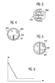
- the substrate holder 3 is pierced with an axial hole 9 which passes in particular through the solid electrode 6 and the upper layer 4 and which makes it possible to supply a network of channels 10 crisscrossed and hollowed out on the upper surface 2 into a gas such as helium or nitrogen which circulates therein in particular to promote cooling or detachment.
- a gas such as helium or nitrogen which circulates therein in particular to promote cooling or detachment.
- the pressure obtained above the filiform electrode 5 is equal to 0.85 Po if the electrode filiform 5 extends under 8% of the surface S of the substrate 1, the solid electrode 6 extending under the remaining 92%.
- the holding force is approximately 0.07 PoS, the contribution of the area above the solid electrode 6 being almost negligible.
- the pressure would be uniform over the entire substrate 1 but only equal to 0.25 Po, and for a holding force of 0.25 PoS, if two concentric electrodes of equal surfaces were used. This is one of the reasons for the interest of very different areas. A report of at least 5 is advised although no precise limit can be given.
- the substrate 1 is brought to the plasma potential. It also forms with the solid electrode 6 a planar capacitor.
- the electrostatic forces in place are both large and almost uniform over the entire substrate 1, which guarantees its flatness and therefore good thermal contact. It is not difficult to create a potential difference between the plasma and the solid electrode 6 sufficient to obtain the desired contact pressure (for example 500 g / cm2 of silicon).
- the much greater heat transmitted to the substrate 1 (of the order of five watts per square centimeter) is therefore removed quickly and uniformly by a large heat exchange surface because there is no yawning between the upper surface 2 of the door.
- the periphery of the substrate 1 which extends above the filiform electrode 5 is not necessarily kept in firm contact, but this drawback is immaterial because this part normally corresponds to a non-useful area of negligible surface.
Landscapes
- Container, Conveyance, Adherence, Positioning, Of Wafer (AREA)
- Chemical Vapour Deposition (AREA)
Applications Claiming Priority (2)
| Application Number | Priority Date | Filing Date | Title |
|---|---|---|---|
| FR9004728A FR2661039B1 (fr) | 1990-04-12 | 1990-04-12 | Porte-substrat electrostatique. |
| FR9004728 | 1990-04-12 |
Publications (2)
| Publication Number | Publication Date |
|---|---|
| EP0452222A1 true EP0452222A1 (de) | 1991-10-16 |
| EP0452222B1 EP0452222B1 (de) | 1997-01-08 |
Family
ID=9395718
Family Applications (1)
| Application Number | Title | Priority Date | Filing Date |
|---|---|---|---|
| EP91400977A Expired - Lifetime EP0452222B1 (de) | 1990-04-12 | 1991-04-11 | Elektrostatischer Substrathalter |
Country Status (3)
| Country | Link |
|---|---|
| EP (1) | EP0452222B1 (de) |
| DE (1) | DE69123995T2 (de) |
| FR (1) | FR2661039B1 (de) |
Cited By (29)
| Publication number | Priority date | Publication date | Assignee | Title |
|---|---|---|---|---|
| DE4107752A1 (de) * | 1990-03-13 | 1991-09-26 | Fuji Electric Co Ltd | Elektrostatische einspannvorrichtung fuer ein scheibenfoermiges substrat |
| EP0541400A3 (en) * | 1991-11-07 | 1993-06-30 | Varian Associates, Inc. | Anti-stick electrostatic chuck for a low pressure environment |
| WO1994020984A1 (en) * | 1993-03-08 | 1994-09-15 | Wolfowitz, Steven, Alan | Non-adhesive ecologically-pure electroadhesion method of clamping and fixing materials |
| EP0635869A1 (de) * | 1993-04-22 | 1995-01-25 | Applied Materials, Inc. | Halbleiterbehandlungsvorrichtung, Verfahren zur Herstellung und Verwendung desselben |
| EP0635870A1 (de) * | 1993-07-20 | 1995-01-25 | Applied Materials, Inc. | Eine elektrostatische Halteplatte mit einer gerillten Fläche |
| EP0634786A3 (de) * | 1993-07-15 | 1995-02-01 | Applied Materials Inc | |
| EP0644578A3 (de) * | 1993-09-16 | 1995-04-19 | Hitachi Ltd | |
| EP0601788A3 (de) * | 1992-12-02 | 1995-05-24 | Applied Materials Inc | Electrostatische Haltevorrichtung benutzbar in Hochdensitätsplasma. |
| EP0660378A1 (de) * | 1993-12-20 | 1995-06-28 | International Business Machines Corporation | Elektrostatische Halteplatte mit Isolator aus Oxiden |
| WO1995020838A1 (en) * | 1994-01-31 | 1995-08-03 | Applied Materials, Inc. | Electrostatic chuck with conformal insulator film |
| EP0683505A1 (de) * | 1994-05-18 | 1995-11-22 | Applied Materials, Inc. | Suszeptor nach einem Modell um die elektrostatische Kraft zu reduzieren |
| US5548470A (en) * | 1994-07-19 | 1996-08-20 | International Business Machines Corporation | Characterization, modeling, and design of an electrostatic chuck with improved wafer temperature uniformity |
| US5583736A (en) * | 1994-11-17 | 1996-12-10 | The United States Of America As Represented By The Department Of Energy | Micromachined silicon electrostatic chuck |
| US5631803A (en) * | 1995-01-06 | 1997-05-20 | Applied Materials, Inc. | Erosion resistant electrostatic chuck with improved cooling system |
| US5656093A (en) * | 1996-03-08 | 1997-08-12 | Applied Materials, Inc. | Wafer spacing mask for a substrate support chuck and method of fabricating same |
| US5729423A (en) * | 1994-01-31 | 1998-03-17 | Applied Materials, Inc. | Puncture resistant electrostatic chuck |
| US5761023A (en) * | 1996-04-25 | 1998-06-02 | Applied Materials, Inc. | Substrate support with pressure zones having reduced contact area and temperature feedback |
| US5764471A (en) * | 1996-05-08 | 1998-06-09 | Applied Materials, Inc. | Method and apparatus for balancing an electrostatic force produced by an electrostatic chuck |
| US5801915A (en) * | 1994-01-31 | 1998-09-01 | Applied Materials, Inc. | Electrostatic chuck having a unidirectionally conducting coupler layer |
| US5810933A (en) * | 1996-02-16 | 1998-09-22 | Novellus Systems, Inc. | Wafer cooling device |
| US5825607A (en) * | 1996-05-08 | 1998-10-20 | Applied Materials, Inc. | Insulated wafer spacing mask for a substrate support chuck and method of fabricating same |
| US5870271A (en) * | 1997-02-19 | 1999-02-09 | Applied Materials, Inc. | Pressure actuated sealing diaphragm for chucks |
| US5885469A (en) * | 1996-11-05 | 1999-03-23 | Applied Materials, Inc. | Topographical structure of an electrostatic chuck and method of fabricating same |
| US6104596A (en) * | 1998-04-21 | 2000-08-15 | Applied Materials, Inc. | Apparatus for retaining a subtrate in a semiconductor wafer processing system and a method of fabricating same |
| US6278600B1 (en) | 1994-01-31 | 2001-08-21 | Applied Materials, Inc. | Electrostatic chuck with improved temperature control and puncture resistance |
| EP0993024A3 (de) * | 1998-09-29 | 2002-07-17 | Ngk Insulators, Ltd. | Elektrostatischer Halter |
| US6524428B2 (en) | 1993-09-16 | 2003-02-25 | Hitachi, Ltd. | Method of holding substrate and substrate holding system |
| US6598559B1 (en) | 2000-03-24 | 2003-07-29 | Applied Materials, Inc. | Temperature controlled chamber |
| EP1548502A1 (de) * | 2003-12-15 | 2005-06-29 | ASML Netherlands BV | Lithographischer Apparat und Verfahren zur Herstellung einer Vorrichtung |
Families Citing this family (3)
| Publication number | Priority date | Publication date | Assignee | Title |
|---|---|---|---|---|
| FR2724269B1 (fr) | 1994-09-06 | 1996-10-18 | Commissariat Energie Atomique | Porte-substrat electrostatique |
| EP1498777A1 (de) | 2003-07-15 | 2005-01-19 | ASML Netherlands B.V. | Substrathalter und lithographischer Projektionsapparat |
| WO2025201814A1 (en) * | 2024-03-29 | 2025-10-02 | Asml Netherlands B.V. | An electrostatic clamp |
Citations (4)
| Publication number | Priority date | Publication date | Assignee | Title |
|---|---|---|---|---|
| EP0049588A2 (de) * | 1980-09-30 | 1982-04-14 | Fujitsu Limited | Verfahren und Vorrichtung zum Trockenätzen und darin benutzte Halterungsvorrichtung |
| EP0138254A1 (de) * | 1983-09-30 | 1985-04-24 | Philips Electronics Uk Limited | Elektrostatische Haltevorrichtung und Verfahren zum Beschicken |
| EP0171011A2 (de) * | 1984-07-31 | 1986-02-12 | Kabushiki Kaisha Tokuda Seisakusho | Elektrostatische Haltevorrichtung |
| EP0260150A2 (de) * | 1986-09-12 | 1988-03-16 | Kabushiki Kaisha Tokuda Seisakusho | Vorrichtung zur Vakuumbehandlung, in der die Temperatur geregelt werden kann |
Family Cites Families (1)
| Publication number | Priority date | Publication date | Assignee | Title |
|---|---|---|---|---|
| JPS60261377A (ja) * | 1984-06-08 | 1985-12-24 | Nippon Telegr & Teleph Corp <Ntt> | 静電チャックの製造方法 |
-
1990
- 1990-04-12 FR FR9004728A patent/FR2661039B1/fr not_active Expired - Fee Related
-
1991
- 1991-04-11 EP EP91400977A patent/EP0452222B1/de not_active Expired - Lifetime
- 1991-04-11 DE DE69123995T patent/DE69123995T2/de not_active Expired - Fee Related
Patent Citations (4)
| Publication number | Priority date | Publication date | Assignee | Title |
|---|---|---|---|---|
| EP0049588A2 (de) * | 1980-09-30 | 1982-04-14 | Fujitsu Limited | Verfahren und Vorrichtung zum Trockenätzen und darin benutzte Halterungsvorrichtung |
| EP0138254A1 (de) * | 1983-09-30 | 1985-04-24 | Philips Electronics Uk Limited | Elektrostatische Haltevorrichtung und Verfahren zum Beschicken |
| EP0171011A2 (de) * | 1984-07-31 | 1986-02-12 | Kabushiki Kaisha Tokuda Seisakusho | Elektrostatische Haltevorrichtung |
| EP0260150A2 (de) * | 1986-09-12 | 1988-03-16 | Kabushiki Kaisha Tokuda Seisakusho | Vorrichtung zur Vakuumbehandlung, in der die Temperatur geregelt werden kann |
Non-Patent Citations (1)
| Title |
|---|
| PATENT ABSTRACTS OF JAPAN, vol. 10, no. 133 (E-404)[2190] 17 mai 1986; & JP-A-60 261 377 (NIPPON DENSHIN DENWA KOSHA) 24 décembre 1985, * |
Cited By (50)
| Publication number | Priority date | Publication date | Assignee | Title |
|---|---|---|---|---|
| DE4107752A1 (de) * | 1990-03-13 | 1991-09-26 | Fuji Electric Co Ltd | Elektrostatische einspannvorrichtung fuer ein scheibenfoermiges substrat |
| DE4107752C2 (de) * | 1990-03-13 | 2003-04-24 | Fuji Electric Co Ltd | Elektrostatische Einspannvorrichtung für ein scheibenförmiges Substrat |
| EP0541400A3 (en) * | 1991-11-07 | 1993-06-30 | Varian Associates, Inc. | Anti-stick electrostatic chuck for a low pressure environment |
| EP0734055A3 (de) * | 1991-11-07 | 1996-11-27 | Varian Associates | Elektrostatische antiklebe Halteplatte für eine Niederdruckumgebung |
| US5539609A (en) * | 1992-12-02 | 1996-07-23 | Applied Materials, Inc. | Electrostatic chuck usable in high density plasma |
| EP0601788A3 (de) * | 1992-12-02 | 1995-05-24 | Applied Materials Inc | Electrostatische Haltevorrichtung benutzbar in Hochdensitätsplasma. |
| US5583737A (en) * | 1992-12-02 | 1996-12-10 | Applied Materials, Inc. | Electrostatic chuck usable in high density plasma |
| WO1994020984A1 (en) * | 1993-03-08 | 1994-09-15 | Wolfowitz, Steven, Alan | Non-adhesive ecologically-pure electroadhesion method of clamping and fixing materials |
| EP0635869A1 (de) * | 1993-04-22 | 1995-01-25 | Applied Materials, Inc. | Halbleiterbehandlungsvorrichtung, Verfahren zur Herstellung und Verwendung desselben |
| EP0634786A3 (de) * | 1993-07-15 | 1995-02-01 | Applied Materials Inc | |
| EP0635870A1 (de) * | 1993-07-20 | 1995-01-25 | Applied Materials, Inc. | Eine elektrostatische Halteplatte mit einer gerillten Fläche |
| US5522131A (en) * | 1993-07-20 | 1996-06-04 | Applied Materials, Inc. | Electrostatic chuck having a grooved surface |
| EP0644578A3 (de) * | 1993-09-16 | 1995-04-19 | Hitachi Ltd | |
| US6610171B2 (en) | 1993-09-16 | 2003-08-26 | Hitachi, Ltd. | Method of holding substrate and substrate holding system |
| US6610170B2 (en) | 1993-09-16 | 2003-08-26 | Hitachi, Ltd. | Method of holding substrate and substrate holding system |
| US6645871B2 (en) | 1993-09-16 | 2003-11-11 | Hitachi, Ltd. | Method of holding substrate and substrate holding system |
| US6899789B2 (en) | 1993-09-16 | 2005-05-31 | Hitachi, Ltd. | Method of holding substrate and substrate holding system |
| US6544379B2 (en) | 1993-09-16 | 2003-04-08 | Hitachi, Ltd. | Method of holding substrate and substrate holding system |
| US6524428B2 (en) | 1993-09-16 | 2003-02-25 | Hitachi, Ltd. | Method of holding substrate and substrate holding system |
| US5985035A (en) * | 1993-09-16 | 1999-11-16 | Hitachi, Ltd. | Method of holding substrate and substrate holding system |
| EP0921559A3 (de) * | 1993-09-16 | 1999-08-04 | Hitachi, Ltd. | Halteverfahren und Haltesystem für ein Substrat |
| US5906684A (en) * | 1993-09-16 | 1999-05-25 | Hitachi, Ltd. | Method of holding substrate and substrate holding system |
| US5792304A (en) * | 1993-09-16 | 1998-08-11 | Hitachi, Ltd. | Method of holding substrate and substrate holding system |
| US5535507A (en) * | 1993-12-20 | 1996-07-16 | International Business Machines Corporation | Method of making electrostatic chuck with oxide insulator |
| EP0660378A1 (de) * | 1993-12-20 | 1995-06-28 | International Business Machines Corporation | Elektrostatische Halteplatte mit Isolator aus Oxiden |
| US5753132A (en) * | 1994-01-31 | 1998-05-19 | Applied Materials, Inc. | Method of making electrostatic chuck with conformal insulator film |
| US5729423A (en) * | 1994-01-31 | 1998-03-17 | Applied Materials, Inc. | Puncture resistant electrostatic chuck |
| WO1995020838A1 (en) * | 1994-01-31 | 1995-08-03 | Applied Materials, Inc. | Electrostatic chuck with conformal insulator film |
| US5801915A (en) * | 1994-01-31 | 1998-09-01 | Applied Materials, Inc. | Electrostatic chuck having a unidirectionally conducting coupler layer |
| US6278600B1 (en) | 1994-01-31 | 2001-08-21 | Applied Materials, Inc. | Electrostatic chuck with improved temperature control and puncture resistance |
| US5986875A (en) * | 1994-01-31 | 1999-11-16 | Applied Materials, Inc. | Puncture resistant electrostatic chuck |
| US5745331A (en) * | 1994-01-31 | 1998-04-28 | Applied Materials, Inc. | Electrostatic chuck with conformal insulator film |
| EP0683505A1 (de) * | 1994-05-18 | 1995-11-22 | Applied Materials, Inc. | Suszeptor nach einem Modell um die elektrostatische Kraft zu reduzieren |
| US5531835A (en) * | 1994-05-18 | 1996-07-02 | Applied Materials, Inc. | Patterned susceptor to reduce electrostatic force in a CVD chamber |
| US5548470A (en) * | 1994-07-19 | 1996-08-20 | International Business Machines Corporation | Characterization, modeling, and design of an electrostatic chuck with improved wafer temperature uniformity |
| US5675471A (en) * | 1994-07-19 | 1997-10-07 | International Business Machines Corporation | Characterization, modeling, and design of an electrostatic chuck with improved wafer temperature uniformity |
| US5583736A (en) * | 1994-11-17 | 1996-12-10 | The United States Of America As Represented By The Department Of Energy | Micromachined silicon electrostatic chuck |
| US5631803A (en) * | 1995-01-06 | 1997-05-20 | Applied Materials, Inc. | Erosion resistant electrostatic chuck with improved cooling system |
| US5810933A (en) * | 1996-02-16 | 1998-09-22 | Novellus Systems, Inc. | Wafer cooling device |
| US5656093A (en) * | 1996-03-08 | 1997-08-12 | Applied Materials, Inc. | Wafer spacing mask for a substrate support chuck and method of fabricating same |
| US5761023A (en) * | 1996-04-25 | 1998-06-02 | Applied Materials, Inc. | Substrate support with pressure zones having reduced contact area and temperature feedback |
| US5764471A (en) * | 1996-05-08 | 1998-06-09 | Applied Materials, Inc. | Method and apparatus for balancing an electrostatic force produced by an electrostatic chuck |
| US5825607A (en) * | 1996-05-08 | 1998-10-20 | Applied Materials, Inc. | Insulated wafer spacing mask for a substrate support chuck and method of fabricating same |
| US5885469A (en) * | 1996-11-05 | 1999-03-23 | Applied Materials, Inc. | Topographical structure of an electrostatic chuck and method of fabricating same |
| US5870271A (en) * | 1997-02-19 | 1999-02-09 | Applied Materials, Inc. | Pressure actuated sealing diaphragm for chucks |
| US6104596A (en) * | 1998-04-21 | 2000-08-15 | Applied Materials, Inc. | Apparatus for retaining a subtrate in a semiconductor wafer processing system and a method of fabricating same |
| EP0993024A3 (de) * | 1998-09-29 | 2002-07-17 | Ngk Insulators, Ltd. | Elektrostatischer Halter |
| US6598559B1 (en) | 2000-03-24 | 2003-07-29 | Applied Materials, Inc. | Temperature controlled chamber |
| EP1548502A1 (de) * | 2003-12-15 | 2005-06-29 | ASML Netherlands BV | Lithographischer Apparat und Verfahren zur Herstellung einer Vorrichtung |
| US7187433B2 (en) | 2003-12-15 | 2007-03-06 | Asml Netherlands B.V. | Electrostatic clamp assembly for a lithographic apparatus |
Also Published As
| Publication number | Publication date |
|---|---|
| DE69123995T2 (de) | 1997-06-26 |
| EP0452222B1 (de) | 1997-01-08 |
| DE69123995D1 (de) | 1997-02-20 |
| FR2661039A1 (fr) | 1991-10-18 |
| FR2661039B1 (fr) | 1997-04-30 |
Similar Documents
| Publication | Publication Date | Title |
|---|---|---|
| EP0452222B1 (de) | Elektrostatischer Substrathalter | |
| FR2579910A1 (de) | ||
| EP0851465A1 (de) | Verfahren zum Trennen von mindestens zwei Elementen einer Struktur, die durch Ionenimplantation verbunden sind | |
| EP1055047B1 (de) | Herstellungsverfahren einer evakuierten isolierverglasung | |
| FR2813993A1 (fr) | Dispositif de semi-conducteur | |
| EP0334709B1 (de) | Vorrichtung für die selektive Verzinnungen der Leiterbahnen eines Trägers einer integrierten Schaltung mit hoher Dichte und ein eine derartige Vorrichtung verwendendes Verzinnungsverfahren | |
| CA2374143C (fr) | Substrat pour circuit electronique de puissance et module electronique de puissance utilisant un tel substrat | |
| FR2534743A1 (fr) | Procede de fabrication de plusieurs composants semi-conducteurs sur une couche conductrice commune et dispositif obtenu, en particulier diode hyperfrequence | |
| EP1635381A2 (de) | Dünnstsubstrathalter | |
| EP2115181A2 (de) | Verfahren zur montage von mindestens zwei platten und verwendung dieses verfahrens zur herstellung einer ionensputteranordnung | |
| FR2724269A1 (fr) | Porte-substrat electrostatique | |
| WO2013093238A1 (fr) | Support comportant un porte-substrat électrostatique | |
| EP0793269B1 (de) | Halbleiteranordnung mit einem auf einen Träger gelöteten Chip mit Durchgangsleitungen und Herstellungsverfahren dafür | |
| CA2350653C (fr) | Procede de maintien electrostatique et dispositif de mise en oeuvre du procede | |
| EP3948941B1 (de) | Verfahren zur herstellung eines halbleiter-auf-isolator-substrats | |
| EP0242667B1 (de) | Lötwerkzeug für elektronische Vorrichtungen | |
| EP1889342A2 (de) | Eine laservorrichtung bildender laserdiodenstapel | |
| FR2601818A1 (fr) | Montage d'un dispositif semiconducteur sur une embase | |
| EP0545748A1 (de) | Anordnung zur Zuführung einer Spannung auf einen Substrathalter | |
| FR3104175A1 (fr) | Nacelle pour dispositif de depot chimique en phase vapeur assiste par plasma | |
| FR2702329A1 (fr) | Procédé de fermeture hermétique d'enceinte en particulier d'enceinte contenant des circuits microélectroniques, et enceinte ainsi obtenue. | |
| WO2025185899A1 (fr) | Procede d'assemblage de deux substrats par adhesion moleculaire | |
| FR3160054A1 (fr) | Procede d’assemblage de deux substrats par adhesion moleculaire | |
| FR2587732A1 (fr) | Reacteur de depot chimique en phase vapeur assiste par plasma | |
| WO2025026895A1 (fr) | Substrat semiconducteur détachable en carbure de silicium polycristallin |
Legal Events
| Date | Code | Title | Description |
|---|---|---|---|
| PUAI | Public reference made under article 153(3) epc to a published international application that has entered the european phase |
Free format text: ORIGINAL CODE: 0009012 |
|
| AK | Designated contracting states |
Kind code of ref document: A1 Designated state(s): CH DE FR GB LI |
|
| 17P | Request for examination filed |
Effective date: 19920324 |
|
| 17Q | First examination report despatched |
Effective date: 19940614 |
|
| GRAG | Despatch of communication of intention to grant |
Free format text: ORIGINAL CODE: EPIDOS AGRA |
|
| GRAH | Despatch of communication of intention to grant a patent |
Free format text: ORIGINAL CODE: EPIDOS IGRA |
|
| GRAH | Despatch of communication of intention to grant a patent |
Free format text: ORIGINAL CODE: EPIDOS IGRA |
|
| GRAA | (expected) grant |
Free format text: ORIGINAL CODE: 0009210 |
|
| AK | Designated contracting states |
Kind code of ref document: B1 Designated state(s): CH DE FR GB LI |
|
| REG | Reference to a national code |
Ref country code: CH Ref legal event code: EP |
|
| REF | Corresponds to: |
Ref document number: 69123995 Country of ref document: DE Date of ref document: 19970220 |
|
| GBT | Gb: translation of ep patent filed (gb section 77(6)(a)/1977) |
Effective date: 19970403 |
|
| PLBE | No opposition filed within time limit |
Free format text: ORIGINAL CODE: 0009261 |
|
| STAA | Information on the status of an ep patent application or granted ep patent |
Free format text: STATUS: NO OPPOSITION FILED WITHIN TIME LIMIT |
|
| 26N | No opposition filed | ||
| PGFP | Annual fee paid to national office [announced via postgrant information from national office to epo] |
Ref country code: GB Payment date: 19980402 Year of fee payment: 8 |
|
| PGFP | Annual fee paid to national office [announced via postgrant information from national office to epo] |
Ref country code: DE Payment date: 19980404 Year of fee payment: 8 |
|
| PGFP | Annual fee paid to national office [announced via postgrant information from national office to epo] |
Ref country code: CH Payment date: 19980422 Year of fee payment: 8 |
|
| PG25 | Lapsed in a contracting state [announced via postgrant information from national office to epo] |
Ref country code: GB Free format text: LAPSE BECAUSE OF NON-PAYMENT OF DUE FEES Effective date: 19990411 |
|
| PGFP | Annual fee paid to national office [announced via postgrant information from national office to epo] |
Ref country code: FR Payment date: 19990427 Year of fee payment: 9 |
|
| PG25 | Lapsed in a contracting state [announced via postgrant information from national office to epo] |
Ref country code: LI Free format text: LAPSE BECAUSE OF NON-PAYMENT OF DUE FEES Effective date: 19990430 Ref country code: CH Free format text: LAPSE BECAUSE OF NON-PAYMENT OF DUE FEES Effective date: 19990430 |
|
| GBPC | Gb: european patent ceased through non-payment of renewal fee |
Effective date: 19990411 |
|
| REG | Reference to a national code |
Ref country code: CH Ref legal event code: PL |
|
| PG25 | Lapsed in a contracting state [announced via postgrant information from national office to epo] |
Ref country code: DE Free format text: LAPSE BECAUSE OF NON-PAYMENT OF DUE FEES Effective date: 20000201 |
|
| PG25 | Lapsed in a contracting state [announced via postgrant information from national office to epo] |
Ref country code: FR Free format text: LAPSE BECAUSE OF NON-PAYMENT OF DUE FEES Effective date: 20001229 |
|
| REG | Reference to a national code |
Ref country code: FR Ref legal event code: ST |