EP0452747A2 - Circuit d'insolation des intérférences des lignes de masse - Google Patents
Circuit d'insolation des intérférences des lignes de masse Download PDFInfo
- Publication number
- EP0452747A2 EP0452747A2 EP91105408A EP91105408A EP0452747A2 EP 0452747 A2 EP0452747 A2 EP 0452747A2 EP 91105408 A EP91105408 A EP 91105408A EP 91105408 A EP91105408 A EP 91105408A EP 0452747 A2 EP0452747 A2 EP 0452747A2
- Authority
- EP
- European Patent Office
- Prior art keywords
- lead
- output
- supply voltage
- ground
- circuit
- Prior art date
- Legal status (The legal status is an assumption and is not a legal conclusion. Google has not performed a legal analysis and makes no representation as to the accuracy of the status listed.)
- Withdrawn
Links
Images


Classifications
-
- H—ELECTRICITY
- H03—ELECTRONIC CIRCUITRY
- H03K—PULSE TECHNIQUE
- H03K19/00—Logic circuits, i.e. having at least two inputs acting on one output; Inverting circuits
- H03K19/003—Modifications for increasing the reliability for protection
- H03K19/00346—Modifications for eliminating interference or parasitic voltages or currents
- H03K19/00353—Modifications for eliminating interference or parasitic voltages or currents in bipolar transistor circuits
-
- H—ELECTRICITY
- H03—ELECTRONIC CIRCUITRY
- H03K—PULSE TECHNIQUE
- H03K21/00—Details of pulse counters or frequency dividers
- H03K21/08—Output circuits
Definitions
- This invention relates to integrated circuits and more particularly to output buffer stages and the fall time of such output stages when the output voltage switches from a high to a low voltage.
- Figure 1 is a diagram depicting a typical integrated circuit package 100 including an integrated circuit which has a plurality of output buffers 103-1 through 103-N.
- the ground lead of output buffers 103-1 through 103-N are connected to external ground 12 via a lead of package 100 which has associated therewith inductance 101.
- Each output buffer 103-1 through 103-N is connected to an associated load 112-1 through 112-N, respectively.
- inductance 101 causes ground bounce, i.e., an increase in the effective ground voltage above ground 102, when there is a change in the amount of current flowing through inductor 101. If for example output buffer 103-1 is sinking current from load 112-1 in a steady state condition, load 112-1 is held to a voltage substantially equal to the voltage of ground 102. If then one or more of the other output buffers switches in order to sink additional current through inductor 101, the "ground" voltage applied to load 112-1 will rise in voltage during the transient increase in current through inductor 101.
- FIG. 2 is a schematic diagram of a typical prior art medium speed output buffer.
- An input signal is applied to node N21 in order to control output pull up transistor 233 and output pull down transistor 235 which in turn source and sink, respectively, current to load 212.
- transistor 222 With a logical one input signal applied to node N21, transistor 222 turns on, causing diode 224 to reverse bias, causing pull up transistor 225 to supply base drive to transistor 226.
- Transistor 226 thus turns on, thereby turning off transistor 229, and in turn turning on phase splitter transistor 232.
- phase splitter transistor 232 With phase splitter transistor 232 turned on, pull up transistor 233 is turned off and pull down transistor is turned on, sinking current I load from load 212 through inductor 201 to ground 202.
- medium speed circuit 200 includes node N21 having a relatively large time constant, since capacitor 220 and pull up resistor 221 are relatively large. Circuit 200 also includes node N22 at the base of phase splitter transistor 232, which has a relatively small time constant, due to the rather small parasitic capacitance on node N22.
- FIG 3 is a circuit diagram of a typical prior art high speed output buffer.
- High speed output buffer 300 is similar to the medium speed output buffer 200 of Figure 2 except that the inversions provided by transistors 226 and 229 of Figure 2 are eliminated. This results in node N32 having a relatively large effective time constant, since node N32 follows node N31 through transistor 332 and diode 324. This has the effect of slowing the high to low transition of the output signal applied to load 312, while providing a low propagation delay.
- inductor 301 acts as a feedback impedance to the common emitter amplifier formed by transistors 332 and 335. Since node N32 has a large RC time constant, the voltage on node N32 acts as a small signal to the common emitter amplifier. The effect of the feedback impedance provided by inductor 301 reduces circuit gain and thus the output edge rate.
- Figure 5 is a diagram depicting the waveforms associates with high speed output buffer circuit 300 of Figure 3, showing a smaller propagation delay than that of Figure 4, but with an increased percentage of the total delay due to inductance effects.
- Figure 6 depicts a prior art integrated circuit lead frame 60 including two separate ground leads 61 and 62 for separate connections of grounds on an integrated circuit placed within cavity 64 of lead frame 60, for ultimate connection at pin 63 to a circuit ground.
- Such package has been used in the past in order to minimize ground noise problems.
- Figure 7 is a schematic diagram depicting a model of a typical prior art output circuit.
- a novel output buffer circuit which advantageously uses a simple integrated circuit package including two separate ground leads for connection to an externally supplied ground voltage.
- the relatively large pull down current which passes through the pull down transistor of one of more output buffers is fed through a first ground lead of the lead frame to the external ground and the remaining circuitry is connected to the external ground through the second ground lead of the lead frame. In this manner, the transients in the pull down current will cause ground bounce which affects the pull down transistor only, and not the remaining components of the output buffer.
- the amount of ground bounce is controlled to provide a desired characteristic of the output transition.
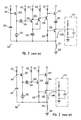
- FIG. 8 is a schematic diagram of one embodiment of an output buffer constructed in accordance with the teachings of this invention.
- Output buffer 800 includes ground inductance 803-1, corresponding to lead 61 of the integrated circuit package shown in Figure 6, for connecting external ground 802 to the driver circuitry of output buffer 800.
- Output buffer 800 also includes a second inductor 803-2 corresponding to lead 62 of the integrated circuit package shown in Figure 6 for connecting output pull down transistor 835 to external ground 802.
- Reference supply 882 provides a bias voltage V ref to the base of transistor 880 which is connected in a common emitter configuration with transistor 822 to current source 823. With a high signal applied to input node N81, transistor 822 turns on, causing transistor 880 to turn off, raising node N82 high.
- phase splitter transistor 832 This causes phase splitter transistor 832 to turn on, turning off output pull up transistor 833, and turning on output pulldown transistor 835.
- This causes pull down current I load to be sunk from load 812 through pull down transistor 835, through inductor 803-2, to ground 802.
- the ground bounce caused by inductor 803-2 is applied only to the emitter of output pull down transistor 835, and does not affect the components which are connected to ground through inductor 803-1 since there is no significant transient current through inductor 803-1 at this time.
- a small time constant and therefore a fast input edge rate is provided at node N82 due to its low capacitance, thereby allowing the high to low transition of the output voltage to be very rapid, thereby enhancing switching speed. Furthermore, this small time constant is provided at node N82 without the need for additional inversions between nodes N81 and N82, as is the case with the prior art medium speed output buffer circuit of Figure 2. Thus, without additional inversions between nodes N81 and N82, the propagation delay is reduced as compared with medium speed circuit 200 Figure 2.
- Figure 7 shows a portion of an output pull down transistor circuit 700 when pull down current I load is being conducted through pull down transistor 704 through package inductance 706 to ground 706.
- L dI/dt is small, limiting the range of charge removal from the output load, and therefore limiting the output edge rate.
- voltage V1 limits di/dt and therefore the speed of the high to low transition of the output voltage applied to load 707.
- V out is the output voltage applied to load 707, in order to provide maximum output switching speed.
- ground bounce should be maximized and the input edge rate should be maximized.
- the amount of ground bounce that a user of such a circuit can tolerate.
- ground bounce is desirably increased, in contrast to the thinking of the prior art. In order to achieve a distinct advantage, i.e., a very rapid high to low transition of the output voltage applied to the load.
- means is provided to control the voltage excursion on nodes N82 or N83, or means to control the rate at which the voltage are nodes N82 or N83.
- Such means include, for example, clamping the desired node to quiet ground 899, for example through one or more diodes or transistors.
- output edge rate/ground bounce is controlled by adding a capacitance in parallel with ground inductance 803-2, preferably in an amount equal to the sum of the load capacitances connected to the plurality of output buffers contained on an integrated circuit.
- a capacitance in parallel with ground inductance 803-2 preferably in an amount equal to the sum of the load capacitances connected to the plurality of output buffers contained on an integrated circuit.
- a smaller value of capacitance is connected to the base of transistors 832 or 835 and reflected through transistor 832 to inductor 803-2, thereby providing an effective capacitance equal to the value of the capacitance multiplied by the beta of transistor 835.
- FIG. 9 is a schematic diagram of another embodiment of an output pull down circuit constructed in accordance with the teachings of this invention.
- Output pull down circuit 900 of Figure 9 is similar to that of Figure 8, but includes transistor 990 and capacitor 991 in order to provide a transient current between the base of transistor 932 and inductor 903-2.
- Circuit elements 990 and 991 serve to prevent phase splitter transistor 932 from turning on during a brief period of time during which the emitter voltage of output pull down transistor 935 falls below ground 902. This occurs due to changes in ground current through other output circuits contained on the same integrated circuit. Such below-ground emitter voltage would ordinarily cause phase splitter transistor 932 to turn on even with relatively low voltage applied to its base.
- capacitor 991 supplies base drive to transistor 990 which turns on briefly in order to ensure that phase splitter transistor 932 remains turned off. Conversely, with the output voltage low, transistor 990 will not turn on even when noisy ground 998 changes voltage due to other output circuits switching current through package inductance 903-2.
- a means is provided to control the voltage excursion on node N92. By preventing the voltage on node N92 from exceeding a predetermined level, the edge rate of the output signal is controlled inversely to the amount of ground bounce permitted on the output signal.
- output edge rate/ground bounce is controlled by adding a capacitance in parallel with ground inductance 903-2, preferably in an amount equal to the sum of the load capacitances connected to the plurality of output buffers contained on an integrated circuit.
- a smaller value of capacitance is connected to the base of transistors 932 or 935 and beta multiplied.
- Figure 10 is a schematic diagram of an alternative embodiment of this invention, which is similar to that shown in Figure 9 and includes similar numbering.
- the embodiment of Figure 10 includes transistors 1001 and 1003, resistor 1002, and diode 1004 in order to prevent transistor 932 from inadvertently turning on when output terminal 917 is high. This may occur when noisy ground voltage present on node 998 glitches low with respect to quiet ground voltage present on node 999, for example when current I load in this or other output stages on the same integrated circuit begin to conduct an increased amount of current. During this time, the noisy ground voltage on node 998 goes lower with respect to the quiet ground voltage on node 999, thereby increasing the voltage across the base-emitter junction of transistor 932.
- transistor 1003 turns on due to its decreased emitter voltage, pulling down the base of transistor 932, preventing it from inadvertently turning on.
- Transistor 1001 and resistor 1002 provide base drive to transistor 1003, and diode 1004 clamps the base voltage of transistor 1003 to approximately 0.6 volts above the quiet ground voltage present on node 999.
Landscapes
- Physics & Mathematics (AREA)
- Engineering & Computer Science (AREA)
- Computer Hardware Design (AREA)
- Computing Systems (AREA)
- General Engineering & Computer Science (AREA)
- Mathematical Physics (AREA)
- Logic Circuits (AREA)
- Electronic Switches (AREA)
Applications Claiming Priority (2)
| Application Number | Priority Date | Filing Date | Title |
|---|---|---|---|
| US07/512,786 US5089721A (en) | 1990-04-20 | 1990-04-20 | Ground bounce isolation and high speed output circuit |
| US512786 | 1990-04-20 |
Publications (2)
| Publication Number | Publication Date |
|---|---|
| EP0452747A2 true EP0452747A2 (fr) | 1991-10-23 |
| EP0452747A3 EP0452747A3 (en) | 1991-12-04 |
Family
ID=24040559
Family Applications (1)
| Application Number | Title | Priority Date | Filing Date |
|---|---|---|---|
| EP19910105408 Withdrawn EP0452747A3 (en) | 1990-04-20 | 1991-04-05 | Ground bounce isolation network |
Country Status (4)
| Country | Link |
|---|---|
| US (1) | US5089721A (fr) |
| EP (1) | EP0452747A3 (fr) |
| JP (1) | JPH04229717A (fr) |
| KR (1) | KR0182286B1 (fr) |
Cited By (1)
| Publication number | Priority date | Publication date | Assignee | Title |
|---|---|---|---|---|
| CN108270423A (zh) * | 2018-01-26 | 2018-07-10 | 广东美的制冷设备有限公司 | Igbt模块的驱动保护电路和空调器 |
Families Citing this family (8)
| Publication number | Priority date | Publication date | Assignee | Title |
|---|---|---|---|---|
| US5168176A (en) * | 1991-07-23 | 1992-12-01 | Standard Microsystems Corporation | Apparatus and method to prevent the unsettling of a quiescent, low output channel caused by ground bounce induced by neighboring output channels |
| US5321320A (en) * | 1992-08-03 | 1994-06-14 | Unisys Corporation | ECL driver with adjustable rise and fall times, and method therefor |
| US5506521A (en) * | 1992-08-03 | 1996-04-09 | Unisys Corporation | ECL driver with adjustable rise and fall times, and method therefor |
| US5428303A (en) * | 1994-05-20 | 1995-06-27 | National Semiconductor Corporation | Bias generator for low ground bounce output driver |
| US6127876A (en) * | 1996-10-16 | 2000-10-03 | Texas Instruments Incorporated | Positive ground bounce compensation circuit for bipolar integrated devices |
| US6054874A (en) * | 1997-07-02 | 2000-04-25 | Cypress Semiconductor Corp. | Output driver circuit with switched current source |
| US6084439A (en) * | 1997-07-02 | 2000-07-04 | Cypress Semiconductor Corp. | Peak detector circuit with extended input voltage range |
| KR102749053B1 (ko) | 2021-12-08 | 2025-01-02 | 조하원 | 펌용 환원성 조성물 및 이의 제조방법 |
Family Cites Families (10)
| Publication number | Priority date | Publication date | Assignee | Title |
|---|---|---|---|---|
| US4613771A (en) * | 1984-04-18 | 1986-09-23 | Burroughs Corporation | Integrated circuit having three power bases and proportioned parasitic resistive and capacitive coupling to reduce output noise |
| US4609834A (en) * | 1984-12-24 | 1986-09-02 | Burroughs Corporation | Integrated logic circuit incorporating a module which generates a control signal that cancels switching noise |
| DE3680265D1 (de) * | 1985-02-28 | 1991-08-22 | Sony Corp | Halbleiterschaltungsanordnung. |
| KR960013630B1 (ko) * | 1986-06-30 | 1996-10-10 | 페어차일드 세미콘덕터 코퍼레이션 | 집적회로에서의 접지 변동 감소 장치 |
| US4975603A (en) * | 1986-07-02 | 1990-12-04 | Texas Instruments Incorporated | Method and circuitry for compensating for negative internal ground voltage glitches |
| JPS63234623A (ja) * | 1987-03-23 | 1988-09-29 | Toshiba Corp | 半導体集積回路 |
| JPH01113993A (ja) * | 1987-10-28 | 1989-05-02 | Toshiba Corp | 半導体集積回路 |
| DE3739872A1 (de) * | 1987-11-25 | 1989-06-08 | Texas Instruments Deutschland | Integrierte schaltung |
| US4862018A (en) * | 1987-11-30 | 1989-08-29 | Texas Instruments Incorporated | Noise reduction for output drivers |
| JP2511399Y2 (ja) * | 1988-02-29 | 1996-09-25 | シャープ株式会社 | コンパレ―タ回路 |
-
1990
- 1990-04-20 US US07/512,786 patent/US5089721A/en not_active Expired - Lifetime
-
1991
- 1991-04-05 EP EP19910105408 patent/EP0452747A3/en not_active Withdrawn
- 1991-04-19 JP JP3179066A patent/JPH04229717A/ja active Pending
- 1991-04-19 KR KR1019910006271A patent/KR0182286B1/ko not_active Expired - Fee Related
Cited By (1)
| Publication number | Priority date | Publication date | Assignee | Title |
|---|---|---|---|---|
| CN108270423A (zh) * | 2018-01-26 | 2018-07-10 | 广东美的制冷设备有限公司 | Igbt模块的驱动保护电路和空调器 |
Also Published As
| Publication number | Publication date |
|---|---|
| US5089721A (en) | 1992-02-18 |
| KR910019344A (ko) | 1991-11-30 |
| KR0182286B1 (ko) | 1999-04-15 |
| JPH04229717A (ja) | 1992-08-19 |
| EP0452747A3 (en) | 1991-12-04 |
Similar Documents
| Publication | Publication Date | Title |
|---|---|---|
| US4959563A (en) | Adjustable low noise output circuit | |
| US5118971A (en) | Adjustable low noise output circuit responsive to environmental conditions | |
| US5321319A (en) | High speed CMOS bus driver circuit that provides minimum output signal oscillation | |
| US4791326A (en) | Current controlled solid state switch | |
| JP2759577B2 (ja) | バッファ回路 | |
| EP0164615B1 (fr) | Circuit de commande pour le contrôle de la montée et de la décroissance d'un signal dans des circuits à transistor à effet de champ | |
| US5319260A (en) | Apparatus and method to prevent the disturbance of a quiescent output buffer caused by ground bounce or by power bounce induced by neighboring active output buffers | |
| US4877980A (en) | Time variant drive circuit for high speed bus driver to limit oscillations or ringing on a bus | |
| US5355029A (en) | Staged CMOS output buffer | |
| US5296765A (en) | Driver circuit for sinking current to two supply voltages | |
| JP2567153B2 (ja) | Cmos出力バッファ回路 | |
| US5168176A (en) | Apparatus and method to prevent the unsettling of a quiescent, low output channel caused by ground bounce induced by neighboring output channels | |
| US5089724A (en) | High-speed low-power ECL/NTL circuits with AC-coupled complementary push-pull output stage | |
| US5089721A (en) | Ground bounce isolation and high speed output circuit | |
| JP2941579B2 (ja) | 2乗則クランプ回路 | |
| US6111453A (en) | Power switching device | |
| US5010256A (en) | Gate output driver using slew-rate control | |
| US4924120A (en) | Low noise output circuit | |
| US5148048A (en) | CMOS output circuit having controlled slope | |
| EP0621693A2 (fr) | Circuit BiCMOS d'attaque de sortie | |
| US5517130A (en) | Method and structure for reducing noise in output buffer circuits | |
| US4877975A (en) | Logic circuit having an output signal with a gentle leading edge | |
| JPH03117915A (ja) | 駆動回路 | |
| US4975600A (en) | Bicmos TTL output driver circuit | |
| JPH03147422A (ja) | Ecl回路 |
Legal Events
| Date | Code | Title | Description |
|---|---|---|---|
| PUAI | Public reference made under article 153(3) epc to a published international application that has entered the european phase |
Free format text: ORIGINAL CODE: 0009012 |
|
| PUAL | Search report despatched |
Free format text: ORIGINAL CODE: 0009013 |
|
| AK | Designated contracting states |
Kind code of ref document: A2 Designated state(s): DE FR GB IT |
|
| AK | Designated contracting states |
Kind code of ref document: A3 Designated state(s): DE FR GB IT |
|
| 17P | Request for examination filed |
Effective date: 19920408 |
|
| 17Q | First examination report despatched |
Effective date: 19940715 |
|
| STAA | Information on the status of an ep patent application or granted ep patent |
Free format text: STATUS: THE APPLICATION IS DEEMED TO BE WITHDRAWN |
|
| 18D | Application deemed to be withdrawn |
Effective date: 19950126 |