EP0452955A2 - Capacitor and process for production thereof - Google Patents
Capacitor and process for production thereof Download PDFInfo
- Publication number
- EP0452955A2 EP0452955A2 EP91106343A EP91106343A EP0452955A2 EP 0452955 A2 EP0452955 A2 EP 0452955A2 EP 91106343 A EP91106343 A EP 91106343A EP 91106343 A EP91106343 A EP 91106343A EP 0452955 A2 EP0452955 A2 EP 0452955A2
- Authority
- EP
- European Patent Office
- Prior art keywords
- active agent
- surface active
- film
- liquid crystal
- crystal molecules
- Prior art date
- Legal status (The legal status is an assumption and is not a legal conclusion. Google has not performed a legal analysis and makes no representation as to the accuracy of the status listed.)
- Granted
Links
Images


Classifications
-
- B—PERFORMING OPERATIONS; TRANSPORTING
- B82—NANOTECHNOLOGY
- B82Y—SPECIFIC USES OR APPLICATIONS OF NANOSTRUCTURES; MEASUREMENT OR ANALYSIS OF NANOSTRUCTURES; MANUFACTURE OR TREATMENT OF NANOSTRUCTURES
- B82Y30/00—Nanotechnology for materials or surface science, e.g. nanocomposites
-
- H—ELECTRICITY
- H01—ELECTRIC ELEMENTS
- H01G—CAPACITORS; CAPACITORS, RECTIFIERS, DETECTORS, SWITCHING DEVICES, LIGHT-SENSITIVE OR TEMPERATURE-SENSITIVE DEVICES OF THE ELECTROLYTIC TYPE
- H01G4/00—Fixed capacitors; Processes of their manufacture
- H01G4/002—Details
- H01G4/018—Dielectrics
- H01G4/20—Dielectrics using combinations of dielectrics from more than one of groups H01G4/02 - H01G4/06
-
- B—PERFORMING OPERATIONS; TRANSPORTING
- B82—NANOTECHNOLOGY
- B82Y—SPECIFIC USES OR APPLICATIONS OF NANOSTRUCTURES; MEASUREMENT OR ANALYSIS OF NANOSTRUCTURES; MANUFACTURE OR TREATMENT OF NANOSTRUCTURES
- B82Y10/00—Nanotechnology for information processing, storage or transmission, e.g. quantum computing or single electron logic
-
- H—ELECTRICITY
- H01—ELECTRIC ELEMENTS
- H01G—CAPACITORS; CAPACITORS, RECTIFIERS, DETECTORS, SWITCHING DEVICES, LIGHT-SENSITIVE OR TEMPERATURE-SENSITIVE DEVICES OF THE ELECTROLYTIC TYPE
- H01G4/00—Fixed capacitors; Processes of their manufacture
- H01G4/002—Details
- H01G4/018—Dielectrics
- H01G4/06—Solid dielectrics
- H01G4/14—Organic dielectrics
-
- Y—GENERAL TAGGING OF NEW TECHNOLOGICAL DEVELOPMENTS; GENERAL TAGGING OF CROSS-SECTIONAL TECHNOLOGIES SPANNING OVER SEVERAL SECTIONS OF THE IPC; TECHNICAL SUBJECTS COVERED BY FORMER USPC CROSS-REFERENCE ART COLLECTIONS [XRACs] AND DIGESTS
- Y10—TECHNICAL SUBJECTS COVERED BY FORMER USPC
- Y10T—TECHNICAL SUBJECTS COVERED BY FORMER US CLASSIFICATION
- Y10T29/00—Metal working
- Y10T29/43—Electric condenser making
- Y10T29/435—Solid dielectric type
Definitions
- the dielectric films formed according to the conventional methods are poor in performance and unsatisfactory in reliability.
- the present invention has for its object to provide a small-sized high-performance thin film capacitor at low cost. More specifically, the present invention is aimed at eliminating said prior art defects and relates to a process for producing a capacitor of the type recited, characterized by comprising a step of forming one or more layers of pinhole-free monomolecular film with high dielectric strength on the surface of a thin film electrode according to a chemical adsorption method by using a chlorosilane surface active agent in the dielectric film coating operation in the capacitor production process, and to a capacitor obtained according to said process.
- a process for producing a capacitor characterized by comprising a step of forming a layer of monomolecular film by having a chlorosilane surface active agent in a non-aqueous organic solvent chemically adsorbed on the surface of a metallic film electrode either directly or indirectly with interposition of an appropriate thin film so as to constitute chemical bonding of a siloxane (-SiO-) on said metallic electrode surface.
Landscapes
- Engineering & Computer Science (AREA)
- Chemical & Material Sciences (AREA)
- Nanotechnology (AREA)
- Power Engineering (AREA)
- Crystallography & Structural Chemistry (AREA)
- Microelectronics & Electronic Packaging (AREA)
- Manufacturing & Machinery (AREA)
- Physics & Mathematics (AREA)
- Condensed Matter Physics & Semiconductors (AREA)
- Theoretical Computer Science (AREA)
- Composite Materials (AREA)
- Mathematical Physics (AREA)
- General Physics & Mathematics (AREA)
- Materials Engineering (AREA)
- Fixed Capacitors And Capacitor Manufacturing Machines (AREA)
- Organic Insulating Materials (AREA)
- Liquid Crystal (AREA)
- Addition Polymer Or Copolymer, Post-Treatments, Or Chemical Modifications (AREA)
- Laminated Bodies (AREA)
Abstract
Description
- This invention relates to a capacitor and a process for producing the same. More particularly, it pertains to a method for forming a dielectric thin film on a film electrode in the production of a capacitor.
- For forming a dielectric thin film in the production of capacitors, there have been generally employed a method in which a polyester resin or an epoxy resin is coated on each film electrode and a method in which a polyester film is held between the film electrodes.
- It has become apparent, however, that the dielectric films formed according to the conventional methods are poor in performance and unsatisfactory in reliability. For instance, it has been revealed that according to the conventional coating techniques, when the thickness of the coating film is reduced for enlarging the static capacity, although a satisfactory mechanical strength can be obtained, there arises a risk of forming many pinholes, which leads to a poor yield and greatly deteriorated environmental resistance and dielectric strength of the film.
- In view of these defects of the conventional capacitors, the present invention has for its object to provide a small-sized high-performance thin film capacitor at low cost. More specifically, the present invention is aimed at eliminating said prior art defects and relates to a process for producing a capacitor of the type recited, characterized by comprising a step of forming one or more layers of pinhole-free monomolecular film with high dielectric strength on the surface of a thin film electrode according to a chemical adsorption method by using a chlorosilane surface active agent in the dielectric film coating operation in the capacitor production process, and to a capacitor obtained according to said process.
- In an aspect of the present invention, there is provided a capacitor comprising a dielectric thin film being sandwiched by two layers of thin film electrodes directly or through interposition of a suitable thin film, and lead electrodes connected to said thin film electrodes, said dielectric thin film being a chemically adsorbed monomolecular film or a chemically adsorbed monomolecular built-up film made from a chlorosilane surface active agent.
- In another aspect of the present invention, there is provided a process for producing a capacitor characterized by comprising a step of forming a layer of monomolecular film by having a chlorosilane surface active agent in a non-aqueous organic solvent chemically adsorbed on the surface of a metallic film electrode either directly or indirectly with interposition of an appropriate thin film so as to constitute chemical bonding of a siloxane (-SiO-) on said metallic electrode surface.
- FIG. 1 is a diagrammatic illustration of a thin film electrode for capacitor having a chemical adsorption monomolecular film formed thereon as a dielectric film.
- FIGS. 2 to 8 are diagrammatic representations of the steps shown by magnifying the encircled portion A in FIG. 1 to the molecular level.
- FIG. 9 is a schematic illustration of a process for continuously producing the thin film electrodes for capacitor having a dielectric film formed thereon.
- FIG. 10 is a perspective view of a capacitor produced in an embodiment of the present invention.
- FIG. 11 is a schematic sectional view of a capacitor produced in another embodiment of the present invention.
- The present invention provides a capacitor characterized in that the electrode surface is coated, either directly or through a medium of an appropriate thin film, with a monomolecular chemically adsorbed film or a monomolecular built-up chemically adsorbed film composed of a chlorosilane surface active agent, and a process for producing such a capacitor.
- According to the present invention, by use of chemical adsorption techniques, it is possible to form a thin film dielectric material having high moisture resistance and excellent dielectric strength and to provide a small-sized high-performance capacitor.
- Further, the capacitor of this invention can be produced with ease and at low cost since the production process merely comprises chemical adsorption of a chlorosilane surface active agent on substrates for thin film metallic electrodes.
- In the following, embodiments of this invention are described with reference to FIGS. 1 to 11.
- As shown in FIG. 1, on a film 1 made of a metal (such as Al, Sn, Cu, stainless steel or an alloy containing said metal(s)) designed to serve as a thin film electrode for capacitor and formed by suitable means such as rolling, there is formed a monomolecular
dielectric film 3 made of a chlorosilane surface active agent by having said chlorosilane surface active agent adsorbed on said metallic film 1 by a chemical adsorption method either directly or with the intermedium therebetween of a suitable thin film such as anatural oxide film 2. - Instead of forming said
natural oxide film 2, an electrolytic oxide film may be formed on said metallic film surface by means of electrolytic oxidation or a thin film of an oxide such as Al₂O₃, SnO₂, Cu₂O, or Fe₂O₃ may be formed on said metallic film surface to a thickness of several thousands of angstroms by suitable means such as sputtering deposition. This enables obtainment of a capacitor with even higher performance. - Chemical adsorption in the above operation can be performed in the following way. A hydrophilic metallic film 1 is dried well. Then a solution is prepared by dissolving a chlorosilane surface active agent, e.g., CH₂ = CH-(CH₂)n-SiCl₃ (n represents an integer preferably from 10 up to about 25 for best handling), in an 80:12:8 mixture (by weight ratio) of n-hexadecane, tetrachlorocarbon and chloroform to a concentration of 2 x 10⁻³ to 5 x 10⁻² mol/l, and said metallic film 1 is dipped in this solution at room temperature for about one hour.
- In this process, if an oxide is formed on the surface of said metallic film, it is hydrophilic, and -OH groups are contained in the film surface. Consequently, there takes place a dehydrochlorination reaction between -SiCl₃ groups and -OH groups to form bonding of siloxane (-SiO-), and as a result, as shown in FIG. 2, a
dielectric film 3 made of a monomolecular chemically adsorbedfilm 4 is formed, by the action of said chlorosilane surface active agent, on the surface of the monolayer metallic film 1 to a thickness of 20 - 30 Å. In FIG. 2, numeral 5 denotes a vinyl group. - It is possible to further strengthen and stabilize the
monomolecular film 4 by crosslinking (indicated by 6 in FIG. 3) the vinyl groups (CH₂ = CH-) 5 juxtaposed in the film surface by irradiating it with energy beams such as electron rays, X-rays, γ-rays, ultraviolet rays or ionic rays at a dose of 2 to 5 Mrad in an inert gas such as helium. - If a fluorine-containing surface active agent such as CF₃-(CF₂)n-(CH₂)m-SiCl₃ (m and n are the integers the sum of which is preferably from about 10 to about 25 for best handling quality) or CF₃-(CF₂)n-(CH₂)m-O-SiCl₃ (m and n are the integers the sum of which is preferably from about 10 to about 25 for best handling quality) is used as said chlorosilane surface active agent as shown in FIG. 4, there can be obtained a fluorine-containing adsorption film which is improved in dielectric constant. In FIG. 4, numeral 7 denotes a fluorine atom.
- When it is desired to obtain a film with a slightly greater thickness, a metallic film formed with a single layer of
monomolecular film 4 shown by FIG. 2 is dipped in a THF solution of diborane in a concentration of 1 mol/l at room temperature and then further dipped in a 30% H₂O₂ aqueous solution of sodium hydroxide (NaOH) in a concentration of 0.1 mol/l at room temperature for about one hour to add the hydroxyl groups (OH) 8 to the vinyl groups in the monomolecular film surface as shown in FIG. 5. Thereafter, by repeating the chemical adsorption step using the same reaction solution as used in the above-described adsorbing operation and the OH group addition step, it is possible to obtain a monomolecular built-up film having a desired thickness for use as a dielectric film such as shown in FIG. 6. - Also, in the step of adding hydroxyl groups 8, when radiation such as electron rays, X-rays, γ-rays or ionic rays are applied at a dose of 1-10 Mrad in an atmosphere of an inert gas such as oxygen, nitrogen or water vapor instead of performing the oxidation using a chemical, the active groups such as OH groups, amino groups (NH₂) or imino groups (NH) can be added to the portion of vinyl groups, so that by repeating the chemical adsorption step using the same reaction solution and the addition step by irradiation of energy beams, it is possible to obtain a required film thickness for use as a dielectric film.
- The similar effect can be obtained by conducting a plasma treatment in an active gas atmosphere at 100 W for about 10 minutes instead of applying radiation as in the above embodiment.
- Increase of dielectric constant of the monomolecular chemically adsorbed film can be effected by using as adsorbing reagent a chlorosilane surface active agent having a chemical structure with the molecules with large dipoles such as liquid crystal molecules at a part of the linear carbon chain of the chlorosilane surface active agent.
- If an adsorption reagent prepared by adding trichlorosilyl groups, through a carbon chain, to the molecules of liquid crystal such as nematic liquid crystal or other ferroelectric liquid crystals such as azomethine type, azoxy type or ester type is used as the chlorosilane surface active agent having said liquid crystal molecules, it is possible to form a monomolecular film such as shown in FIG. 7 or FIG. 8. (In the representations of FIGS. 7 and 8, R1 and R2 each represents a substituent.) In FIG. 7, numeral 9 denotes a nematic liquid crystal portion, and in FIG. 8,
numeral 10 denotes a ferroelectric liquid crystal portion. Further, in FIGS. 3 to 8,numerals 4A through 4F denote monomolecular films having different chemical structures. - In this process, if chemical adsorption of the adsorption reagent containing the liquid crystal molecules is conducted after said monomolecular built-up film has been formed, there can be obtained a monomolecular built-up film containing the liquid crystal molecules in the outermost surface.
- Also, when R1 or R2 in the molecule of the chlorosilane surface active agent for chemical adsorption in FIG. 7 or 8 is defined to be a vinyl group, acetylene group or cyano group, it is possible to obtain a monomolecular dielectric built-up film containing the liquid crystal molecules in the whole structure of the monomolecular film by using the above-mentioned monomolecular film build-up method in which chemical adsorption is performed by treatments with a chemical agent or by irradiation.
- Further, since the dielectric film thus obtained has a structure in which the dipoles in the molecules constituting each layer of monomolecular adsorption film are arranged in order, the obtained dielectric film can have a very high dielectric constant.
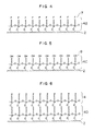
- According to a process where the above-described steps are conducted continuously, as shown in FIG. 9, a metal ingot 11 (e.g., Al or Al-containing alloy) is rolled into a film by a rolling
mill 12, and by using acapstan 13, the film is subjected to the successive treatments in anadsorption tank 14, awashing cistern 15, anelectron ray irradiator 16, anadsorption tank 17, awashing cistern 18 ..., and lastly, after a desired number of layers of monomolecular film were obtained by repeatedly conducting said successive treatments, the thin film electrode forcapacitor 20 comprising the thus formed dielectric film is taken up on adrum 19. This process can be conducted continuously. - In case the natural oxide film is not sufficiently formed on the metallic film surface immediately after rolling, it needs to set, in the rear of the rolling mill, a tank containing an aqueous solution of dilute nitric acid or such for dipping the film therein for a short period of time. It is possible to add a step or steps before the adsorption step, such as a step for electrolytically oxidizing said metallic film surface or a step for sputter-depositing a thin film of an oxide such as SiO₂.
- As for the adsorbing reagent, CH₂ = CH-(CH₂)n-SiOl₃ was used in the above-described embodiment, but it is also possible to use a reagent in which the vinyl group is replaced by acetylene or cyano group, or the trichlorosilyl group is replaced by dichlorosilyl or monochlorosilyl group, or a reaction group is allowed to coexist with said groups.
- Lastly, 2 sheets of thin film electrode formed with said dielectric film are placed one on the other and rolled up as shown in FIG. 10, or 2 sheets of thin film electrode are laminated and press-bonded as shown in FIG. 11, with
lead wires dielectric film 3 by sputtering. - If an electrolyte prepared by dissolving water or boric acid in an amount of a few percents in glycerin or ethylene glycol is held between the electrodes each having a coat of a monomolecular film of monomolecular built-up film, there can be obtained an electrolytic capacitor.
- The present invention provides a capacitor characterized in that the electrode surface is coated, either directly or indirectly by interposing a suitable thin film, with a chemically adsorbed film or a chemically adsorbed monomolecular built-up film composed of a chlorosilane surface active agent, and a process for producing such a capacitor, so that according to this invention it is possible to easily form an extremely thin, high-density faultless dielectric film having a high dielectric constant on the surface of a metallic thin film electrode.
- Also, since this dielectric film is bonded to the electrode surface through a strong siloxane bond, a small-sized high-performance capacitor with excellent moisture resistance and dielectric strength can be offered at notably low cost.
- Further, since the dielectric film formed by said chemical adsorption method can be incorporated with a chemical structure having the molecules with large dipoles (e.g., nematic liquid crystal molecules or ferroelectric liquid crystal molecules), it is possible to control the dielectric constant of the dielectric film.
Claims (20)
- A capacitor comprising a dielectric thin film being sandwiched by two layers of thin film electrodes directly or through interposition of a suitable thin film, and lead electrodes connected to said thin film electrodes, said dielectric thin film being a chemically adsorbed monomolecular film or a chemically adsorbed monomolecular built-up film made from a chlorosilane surface active agent.
- The capacitor according to Claim 1, wherein the chlorosilane surface active agent has a linear carbon chain with 10 to 25 carbon atoms.
- The capacitor according to Claim 1, wherein the chlorosilane surface active agent has at one molecular end thereof a suitable substituent and at the other end molecular thereof a chlorosilyl group.
- The capacitor according to Claim 1, wherein the chlorosilane surface active agent is a compound in which chlorosilyl groups are bonded to part of the liquid crystal molecules through a carbon chain.
- The capacitor according to Claim 4, wherein the liquid crystal molecules are nematic liquid crystal molecules.
- The capacitor according to Claim 4, wherein the liquid crystal molecules are ferroelectric liquid crystal molecules.
- The capacitor according to Claim 6, wherein the ferroelectric liquid crystal is azomethine type, azoxy type or ester type.
- The capacitor according to Claim 6, wherein CH₂ = CH-(CH₂)n-SiCl₃ (wherein n is an integer) is used as the chlorosilane surface active agent.
- The capacitor according to Claim 1, wherein an electrolyte is held between a pair of opposing electrodes made by a chemical adsorption technique method using a chlorosilane surface active agent.
- A process for producing a capacitor, which comprises a step of forming a single layer of monomolecular film on both surfaces of a metallic electrode by letting a chlorosilane surface active agent in a non-aqueous organic solvent be chemically adsorbed on the surface of the electrode-forming film either directly or by interposing therebetween a suitable thin film, and thereby effecting chemical bondings of siloxane.
- The process according to Claim 10, wherein the metallic electrode-forming film is made of Al or an Al-containing alloy.
- The process according to Claim 10, wherein the chlorosilane surface active agent has a linear hydrocarbon chain.
- The process according to Claim 12, wherein the linear carbon chain is terminated at one end thereof with a suitable substituent and at the other end thereof with a chlorosilyl group.
- The process according to Claim 10, wherein the chlorosilane surface active agent has a structure in which chlorosilyl groups are bonded to a part of the liquid crystal molecules through a carbon chain.
- The process according to Claim 14, wherein the liquid crystal molecules are nematic liquid crystal molecules.
- The process according to Claim 14, wherein the liquid crystal molecules are ferroelectric liquid crystal molecules.
- The process according to Claim 16, wherein the ferroelectric liquid crystal is azomethine type, azoxy type or ester type.
- The process according to Claim 10, wherein said chlorosilane surface active agent has at one end thereof a substituent selected from vinyl group, acetylene group and cyano group and has at the other end thereof a chlorosilyl group, said process further compring a step of reacting said substituent by a treatment with a chemical agent for adding a hydroxyl group and then effectuating chemical adsorption of said chlorosilane surface active agent, said step being performed after the step of forming a single layer of monomolecular film by having said chlorosilane surface active agent chemically adsorbed on the metallic electrode surface.
- The process according to Claim 10, wherein the reaction of the substituent is performed by application of radiation or a plasma treatment, and the process includes a step of effecting chemical adsorption of the chlorosilane surface active agent.
- The process according to claim 18, wherein CH₂ = CH(CH₂)n-SiCl₃ (n being an integer) is used as the chlorosilane surface active agent.
Applications Claiming Priority (2)
| Application Number | Priority Date | Filing Date | Title |
|---|---|---|---|
| JP106163/90 | 1990-04-20 | ||
| JP2106163A JPH0752699B2 (en) | 1990-04-20 | 1990-04-20 | Capacitor and its manufacturing method |
Publications (3)
| Publication Number | Publication Date |
|---|---|
| EP0452955A2 true EP0452955A2 (en) | 1991-10-23 |
| EP0452955A3 EP0452955A3 (en) | 1992-08-19 |
| EP0452955B1 EP0452955B1 (en) | 1996-01-31 |
Family
ID=14426616
Family Applications (1)
| Application Number | Title | Priority Date | Filing Date |
|---|---|---|---|
| EP91106343A Expired - Lifetime EP0452955B1 (en) | 1990-04-20 | 1991-04-19 | Capacitor and process for production thereof |
Country Status (4)
| Country | Link |
|---|---|
| US (1) | US5103371A (en) |
| EP (1) | EP0452955B1 (en) |
| JP (1) | JPH0752699B2 (en) |
| DE (1) | DE69116717T2 (en) |
Cited By (4)
| Publication number | Priority date | Publication date | Assignee | Title |
|---|---|---|---|---|
| US5125936A (en) * | 1988-06-03 | 1992-06-30 | Boliden Contech Ab | Emission electrode |
| EP0518219A3 (en) * | 1991-06-14 | 1993-06-16 | Matsushita Electric Industrial Co., Ltd. | Capacitor and method of manufacturing the same |
| EP0523503A3 (en) * | 1991-07-15 | 1994-02-16 | Matsushita Electric Industrial Co Ltd | |
| WO1999023677A1 (en) * | 1997-11-05 | 1999-05-14 | The Secretary Of State For Defence | High storage capacitors |
Families Citing this family (15)
| Publication number | Priority date | Publication date | Assignee | Title |
|---|---|---|---|---|
| CA2060294C (en) * | 1991-02-06 | 2000-01-18 | Kazufumi Ogawa | Chemically absorbed film and method of manufacturing the same |
| JPH0786493B2 (en) * | 1992-04-24 | 1995-09-20 | 松下電器産業株式会社 | Humidity sensor |
| JP3098651B2 (en) * | 1993-03-31 | 2000-10-16 | 松下電器産業株式会社 | Polymer electric device |
| US6265058B1 (en) | 1998-03-11 | 2001-07-24 | Tpl, Inc. | Polymer/paper capacitor film |
| US6483694B1 (en) * | 1999-06-22 | 2002-11-19 | Showa Denko Kabushiki Kaisha | Electrode for electrolytic capacitor, electrolytic capacitor, and manufacturing method therefor |
| US20050067532A1 (en) * | 2003-09-25 | 2005-03-31 | Hindel James T. | Radar absorbing electrothermal de-icer |
| US7658975B2 (en) * | 2003-12-12 | 2010-02-09 | Intel Corporation | Sealing porous dielectric materials |
| DE102004005082B4 (en) * | 2004-02-02 | 2006-03-02 | Infineon Technologies Ag | A capacitor comprising a self-assembled monolayer organic compound dielectric and a method of making the same |
| JP4383227B2 (en) * | 2004-03-31 | 2009-12-16 | 三洋電機株式会社 | Solid electrolytic capacitor and manufacturing method thereof |
| EP1866202B1 (en) * | 2005-04-04 | 2012-11-21 | Goodrich Corporation | Electrothermal deicing apparatus and a dual function heater conductor for use therein |
| US7633450B2 (en) * | 2005-11-18 | 2009-12-15 | Goodrich Corporation | Radar altering structure using specular patterns of conductive material |
| US7455261B2 (en) * | 2006-03-08 | 2008-11-25 | Prudential Co., Ltd. | Tightening mechanism for adjustably setting a tape holder to an immovable state on a tape dispenser |
| JP5831140B2 (en) * | 2011-11-02 | 2015-12-09 | 株式会社村田製作所 | Capacitor |
| US10784049B2 (en) * | 2014-02-03 | 2020-09-22 | Lg Chem, Ltd. | Winding-type stacked body for condenser with high electrostatic capacitance and stacked winding-type condenser using the same |
| JP7673985B2 (en) * | 2020-08-14 | 2025-05-09 | 国立研究開発法人理化学研究所 | Dielectric Materials and Capacitors |
Family Cites Families (4)
| Publication number | Priority date | Publication date | Assignee | Title |
|---|---|---|---|---|
| DE1266671B (en) * | 1964-09-30 | 1968-04-18 | Dr Hans Kuhn | Process for the manufacture of devices for optical and / or electrical purposes, such as thin film capacitors, interference filters and photoresistors |
| JPS5084860A (en) * | 1973-11-30 | 1975-07-09 | ||
| JPS62221103A (en) * | 1986-03-24 | 1987-09-29 | 松下電器産業株式会社 | Capacitor and manufacture of the same |
| JPH0697571B2 (en) * | 1987-12-07 | 1994-11-30 | 信越化学工業株式会社 | Organic high dielectric |
-
1990
- 1990-04-20 JP JP2106163A patent/JPH0752699B2/en not_active Expired - Lifetime
-
1991
- 1991-04-11 US US07/683,857 patent/US5103371A/en not_active Expired - Lifetime
- 1991-04-19 DE DE69116717T patent/DE69116717T2/en not_active Expired - Lifetime
- 1991-04-19 EP EP91106343A patent/EP0452955B1/en not_active Expired - Lifetime
Cited By (7)
| Publication number | Priority date | Publication date | Assignee | Title |
|---|---|---|---|---|
| US5125936A (en) * | 1988-06-03 | 1992-06-30 | Boliden Contech Ab | Emission electrode |
| EP0518219A3 (en) * | 1991-06-14 | 1993-06-16 | Matsushita Electric Industrial Co., Ltd. | Capacitor and method of manufacturing the same |
| EP0523503A3 (en) * | 1991-07-15 | 1994-02-16 | Matsushita Electric Industrial Co Ltd | |
| US5436033A (en) * | 1991-07-15 | 1995-07-25 | Matsushita Electric Industrial Co., Ltd. | Method of manufacturing a polymer ultra thin film electret |
| WO1999023677A1 (en) * | 1997-11-05 | 1999-05-14 | The Secretary Of State For Defence | High storage capacitors |
| GB2346011A (en) * | 1997-11-05 | 2000-07-26 | Secr Defence | High storage capacitors |
| GB2346011B (en) * | 1997-11-05 | 2002-05-22 | Secr Defence | High storage capacitors |
Also Published As
| Publication number | Publication date |
|---|---|
| JPH0752699B2 (en) | 1995-06-05 |
| US5103371A (en) | 1992-04-07 |
| JPH043907A (en) | 1992-01-08 |
| EP0452955B1 (en) | 1996-01-31 |
| DE69116717D1 (en) | 1996-03-14 |
| DE69116717T2 (en) | 1996-08-14 |
| EP0452955A3 (en) | 1992-08-19 |
Similar Documents
| Publication | Publication Date | Title |
|---|---|---|
| EP0452955B1 (en) | Capacitor and process for production thereof | |
| EP0518219A2 (en) | Capacitor and method of manufacturing the same | |
| EP0523503B1 (en) | Ultra thin polymer film electret and method of manufacturing the same | |
| EP0975026A2 (en) | Metal complex useful as sensitizer, dye-sensitized oxide semiconductor electrode and solar cell using same | |
| EP0282188A1 (en) | Recording medium and method of producing the same | |
| EP0599150B1 (en) | Hydrophilic thin coating and method of manufacturing the same | |
| JPH0271873A (en) | Production of monomolecular built-up film | |
| JP2506973B2 (en) | Method of manufacturing optical recording medium | |
| JPH0513530B2 (en) | ||
| Reniers | The development of a transfer mechanism between UHV and electrochemistry environments | |
| Romann et al. | Formation of the bismuth thiolate compound layer on bismuth surface | |
| EP1712298B1 (en) | Organic thin film insulator | |
| US5277772A (en) | Chemical modification of surfaces using heterocyclic azides | |
| JPH0748459A (en) | Ion conductive thin film and manufacturing method thereof | |
| KR102785963B1 (en) | Interstitially mixed self-assembled monolayers and Manufacturing method of the same by ReSEM Method | |
| JPH0629147A (en) | Laminate for laminated film capacitor | |
| JP3074903B2 (en) | Dielectric film for capacitors | |
| JP2617734B2 (en) | Method for manufacturing solid electrolytic capacitor | |
| JPH07192970A (en) | Capacitor and manufacturing method thereof | |
| JPH0560994B2 (en) | ||
| JPH0516087B2 (en) | ||
| JP4084673B2 (en) | Electrolytic capacitor | |
| JPH01275614A (en) | Method for producing polyacetylene or polyacene type ultralong conjugated polymer | |
| JPS6339664A (en) | Method for manufacturing semiconducting or conductive thin films | |
| JPH08124797A (en) | Dielectric thin film, manufacturing method thereof, and capacitor |
Legal Events
| Date | Code | Title | Description |
|---|---|---|---|
| PUAI | Public reference made under article 153(3) epc to a published international application that has entered the european phase |
Free format text: ORIGINAL CODE: 0009012 |
|
| AK | Designated contracting states |
Kind code of ref document: A2 Designated state(s): DE FR GB |
|
| PUAL | Search report despatched |
Free format text: ORIGINAL CODE: 0009013 |
|
| AK | Designated contracting states |
Kind code of ref document: A3 Designated state(s): DE FR GB |
|
| 17P | Request for examination filed |
Effective date: 19920925 |
|
| 17Q | First examination report despatched |
Effective date: 19940725 |
|
| GRAA | (expected) grant |
Free format text: ORIGINAL CODE: 0009210 |
|
| AK | Designated contracting states |
Kind code of ref document: B1 Designated state(s): DE FR GB |
|
| REF | Corresponds to: |
Ref document number: 69116717 Country of ref document: DE Date of ref document: 19960314 |
|
| ET | Fr: translation filed | ||
| PLBE | No opposition filed within time limit |
Free format text: ORIGINAL CODE: 0009261 |
|
| STAA | Information on the status of an ep patent application or granted ep patent |
Free format text: STATUS: NO OPPOSITION FILED WITHIN TIME LIMIT |
|
| 26N | No opposition filed | ||
| REG | Reference to a national code |
Ref country code: GB Ref legal event code: IF02 |
|
| PGFP | Annual fee paid to national office [announced via postgrant information from national office to epo] |
Ref country code: GB Payment date: 20100325 Year of fee payment: 20 |
|
| PGFP | Annual fee paid to national office [announced via postgrant information from national office to epo] |
Ref country code: FR Payment date: 20100521 Year of fee payment: 20 |
|
| PGFP | Annual fee paid to national office [announced via postgrant information from national office to epo] |
Ref country code: DE Payment date: 20100430 Year of fee payment: 20 |
|
| REG | Reference to a national code |
Ref country code: DE Ref legal event code: R071 Ref document number: 69116717 Country of ref document: DE |
|
| REG | Reference to a national code |
Ref country code: GB Ref legal event code: PE20 Expiry date: 20110418 |
|
| PG25 | Lapsed in a contracting state [announced via postgrant information from national office to epo] |
Ref country code: GB Free format text: LAPSE BECAUSE OF EXPIRATION OF PROTECTION Effective date: 20110418 |
|
| PG25 | Lapsed in a contracting state [announced via postgrant information from national office to epo] |
Ref country code: DE Free format text: LAPSE BECAUSE OF EXPIRATION OF PROTECTION Effective date: 20110419 |