EP0453161A2 - Appareil d'enregistrement optique - Google Patents
Appareil d'enregistrement optique Download PDFInfo
- Publication number
- EP0453161A2 EP0453161A2 EP91303148A EP91303148A EP0453161A2 EP 0453161 A2 EP0453161 A2 EP 0453161A2 EP 91303148 A EP91303148 A EP 91303148A EP 91303148 A EP91303148 A EP 91303148A EP 0453161 A2 EP0453161 A2 EP 0453161A2
- Authority
- EP
- European Patent Office
- Prior art keywords
- recording
- optical
- data read
- signal
- light source
- Prior art date
- Legal status (The legal status is an assumption and is not a legal conclusion. Google has not performed a legal analysis and makes no representation as to the accuracy of the status listed.)
- Withdrawn
Links
- 230000003287 optical effect Effects 0.000 title claims abstract description 82
- 238000001514 detection method Methods 0.000 claims abstract description 33
- 239000004065 semiconductor Substances 0.000 claims abstract description 24
- 238000012544 monitoring process Methods 0.000 claims abstract description 6
- 238000005259 measurement Methods 0.000 claims description 17
- 238000013524 data verification Methods 0.000 claims description 3
- 238000010586 diagram Methods 0.000 description 24
- 238000000034 method Methods 0.000 description 8
- KNMAVSAGTYIFJF-UHFFFAOYSA-N 1-[2-[(2-hydroxy-3-phenoxypropyl)amino]ethylamino]-3-phenoxypropan-2-ol;dihydrochloride Chemical compound Cl.Cl.C=1C=CC=CC=1OCC(O)CNCCNCC(O)COC1=CC=CC=C1 KNMAVSAGTYIFJF-UHFFFAOYSA-N 0.000 description 5
- 230000035945 sensitivity Effects 0.000 description 5
- 238000006243 chemical reaction Methods 0.000 description 3
- 230000000694 effects Effects 0.000 description 3
- 230000003252 repetitive effect Effects 0.000 description 3
- 230000004044 response Effects 0.000 description 3
- 230000032683 aging Effects 0.000 description 2
- 230000003247 decreasing effect Effects 0.000 description 2
- 238000005516 engineering process Methods 0.000 description 2
- 238000013459 approach Methods 0.000 description 1
- 230000015572 biosynthetic process Effects 0.000 description 1
- 239000013078 crystal Substances 0.000 description 1
- 238000007599 discharging Methods 0.000 description 1
- 230000006870 function Effects 0.000 description 1
- 230000000977 initiatory effect Effects 0.000 description 1
- 238000007726 management method Methods 0.000 description 1
- 230000010355 oscillation Effects 0.000 description 1
- 239000010453 quartz Substances 0.000 description 1
- 230000000630 rising effect Effects 0.000 description 1
- VYPSYNLAJGMNEJ-UHFFFAOYSA-N silicon dioxide Inorganic materials O=[Si]=O VYPSYNLAJGMNEJ-UHFFFAOYSA-N 0.000 description 1
- 238000012795 verification Methods 0.000 description 1
Images







Classifications
-
- G—PHYSICS
- G11—INFORMATION STORAGE
- G11B—INFORMATION STORAGE BASED ON RELATIVE MOVEMENT BETWEEN RECORD CARRIER AND TRANSDUCER
- G11B7/00—Recording or reproducing by optical means, e.g. recording using a thermal beam of optical radiation by modifying optical properties or the physical structure, reproducing using an optical beam at lower power by sensing optical properties; Record carriers therefor
- G11B7/12—Heads, e.g. forming of the optical beam spot or modulation of the optical beam
- G11B7/125—Optical beam sources therefor, e.g. laser control circuitry specially adapted for optical storage devices; Modulators, e.g. means for controlling the size or intensity of optical spots or optical traces
- G11B7/126—Circuits, methods or arrangements for laser control or stabilisation
-
- G—PHYSICS
- G11—INFORMATION STORAGE
- G11B—INFORMATION STORAGE BASED ON RELATIVE MOVEMENT BETWEEN RECORD CARRIER AND TRANSDUCER
- G11B27/00—Editing; Indexing; Addressing; Timing or synchronising; Monitoring; Measuring tape travel
- G11B27/36—Monitoring, i.e. supervising the progress of recording or reproducing
Definitions
- the present invention relates to optical recording apparatus, and particularly to means for controlling an output from a light source of the apparatus for information recording.
- Figure 2 is a graph showing the relation between light output (P) and drive current (I) for a semi-conductor laser.
- the I-P characteristics of a semi-conductor laser have temperature dependence. That is, at a normal temperature T0, the oscillation threshold current (Ith) is Ith0 and the I-P characteristic is as shown at 106. When the temperature of the semi-conductor laser has risen to T1, the I-P characteristic is shifted as shown at 107.
- the drive current Iw has a fixed value as shown in the Figure at a time of recording, the laser power will drop from P0 to P1 in response to a temperature fluctuation.
- APC automatic power control
- ALPC automatic laser power control
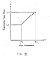
- Figure 3 is a graph showing the relation between a recorded data pulse width and disk temperature when recording is done in a state where the recording power is maintained fixed.
- the recording sensitivity rises and the recorded pits become larger so that the data pulse width increases from L1 to L2.
- This sort of prior technology has a problem in that the recording power ends up slipping away from the most suitable value and the signal quality of the data signal deteriorates.
- the present invention seeks to resolve the problems described above and to provide optical recording apparatus capable of recording information without being affected by fluctuations in the recording sensitivity of a disk resulting from temperature changes and/or ageing.
- optical recording apparatus having an optical head with a laser as a light source, optical output control means for generating signals for controlling the optical output of the light source for information recording, and optical source drive means for driving the light source according to the output of the optical output control means, characterised by data read means for generating data read signals obtained by monitoring recorded pits in a recording medium, and recording state detection means, which detect the state of the recorded pits based on the data read signals and which co-operates with the optical output control means so as to control the optical output of the light source at the time of information recording in dependence upon the state of the recorded pits.
- the state of the data read signals obtained from the recorded pits is monitored by the recording state detection means, and, when the recording power is judged to be excessive, the optical output control means reduces the output of the light source appropriately. Conversely, when the recording power is judged to be too little, the optical output control means increases the output of the light source appropriately. In this way, the output of the light source is controlled to optimise the state of the recorded pits so that information can be continuously recorded with an optimum recording power.
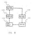
- Figure 1 is a block diagram of optical recording apparatus according to the present invention comprising a semi conductor laser as a light source within an optical head 101.
- the laser records information in the form of pits in an optical disk, and the type of optical disk recording employed may be a write-once type or a magneto-optical or phase change erasable type.
- a drive or write current supplied by optical source drive means 105 is set by optical output control means 104 so that a previously determined recording power is achieved.
- the optical source drive means 105 drive the semi-conductor laser in the optical head 101 to record data.
- data verification is carried out conventionally by checking to see if the data has been written correctly.
- the state of a signal read out by data read means 102 is detected by recording state detection means 103.
- the optical output control means 104 responds by commanding the optical source drive means 105 to increase the drive current for the semi-conductor laser and hence to increase the optical output.
- the data read signal is recognised as being at a value representing a recording power higher than the optimum value, an operation is carried out that is the reverse of the above.
- the recording power is thus constantly controlled by such a sequence so as to have an optimum value.
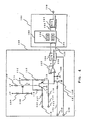
- Figure 4 is a specific circuit diagram of a part of a first embodiment of the recording state detection means 103, comprising pulse width measurement means 139, together with the output control means 104.
- the recording state detection means 103 also comprises bistable means for converting the output from the data read means 102 into a digital signal, but explanation of these bistable means will be omitted because such means can be accomplished with conventional circuit elements, such as comparators.
- a constant current source consists of resistors 108, 109 and 110 and a transistor 111.
- the value of the constant current is assumed to be I.
- This current may be switched by transistors 112 and 113.
- Resistors 114, 115, 116, 117 and 118 impart biases to the two transistors 112 and 113.
- a signal 120, which is a digitised string of data read pulses supplied by the data read means 102, is input at a terminal 119, and similarly a signal 122, which is a digitised string of data read pulses, is input at a terminal 121.
- the signal 120 will be "H” in a pit segment and "L” between pits, and the signal 122 is of opposite phase.
- the transistor 113 turns on, the transistor 112 turns off and the constant current I flows to a condenser 126 in the pit segments.
- the constant current I flows from the collector of the transistor 112 to GND between the pits.
- a transistor 125 is provided for the purpose of discharging the charge stored in the condenser 126 at a time when a re-set signal 124 input from a terminal 123 becomes “H” and makes the transistor 125 turn on.
- V I T/C That is, V is proportional to T.
- the voltage V is converted to digital form by an A/D converter 129 to provide pulse width data 132, an A/D conversion timing signal 131 being input from a terminal 130.
- the A/D conversion is effected in response to the rising edge of the signal 131.
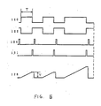
- Figure 5 shows the signal wave forms at several parts of the pulse width measurement means 139 of Figure 4.
- the circuit of the optical output control means 104 in Figure 4 will be explained next.
- the operational functions for recording power control are carried out by a CPU 133.
- the CPU 133 is a one chip structure containing a ROM 134 and a RAM 135.
- the ROM 134 contains a control program and constants.
- the RAM 135 stores data, such as the results of operations, and is used when necessary.
- the CPU 133 compares the pulse width data 132 arriving from the pulse width measurement means 139 against a specified value. When the former is less than the specified value, the CPU 133 outputs data 136 to a D/A converter 137, which effects D/A conversion to supply a laser power control signal from a terminal 138 so that the pulse current at recording time is increased and the recording power becomes greater.
- the pulse width data 132 is greater than the specified value, operations the reverse of those just described are carried out so that the recording power is made smaller.
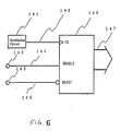
- Figure 6 shows an alternative example of the pulse width measurement means 139 comprising a quartz crystal oscillator 141 for generating a clock signal 142 for a counter 140.
- a signal 144 which is a digitised string of data read pulses supplied by the data read means 102, is input from a terminal 143. This signal becomes "H” at a pit segment, and the counter 140 goes to an enable state at this time.
- a re-set signal 146 for the counter 140 is input from a terminal 145, and when this signal becomes "L", the counter 140 is re-set.
- the output 147 of the counter 140 constitutes data from measurement of the pulse width.
- Figure 7 shows the signal wave forms at each part of the circuit of Figure 6.
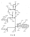
- FIG 8 is a circuit diagram of a part of another embodiment of the recording state detection means 103 of the apparatus of Figure 1, in the form of duty detection means.
- a digital signal 149 provided by the bistable means of the recording state detection means 103 mentioned above, is input at a terminal 148 and a re-set signal is input at a terminal 150.
- a transistor 151 turns on and the charge stored in a condenser 152 is discharged.
- the re-set signal becomes "H” only for a pre-determined time before the state of the data read signal is detected.
- a constant current source comprises resistors 153, 154 and 155 and a transistor 156. The value of the constant current is assumed to be 1.
- a transistor 157 turns on, and base voltage of a transistor 158 attains a value determined by a voltage +V divided by resistors 159 and 160. At this time, current passes through the transistor 158 and charges the condenser 152.
- the transistor 157 turns off, the base of the transistor 158 is fixed at the voltage +V, and the transistor 158 is turned off so that the current I does not flow into the condenser 152.
- the voltage V0 retains the value that it had previously and the output 162 is converted to a digital signal 164 by an A/D converter 163.
- the optical output control means 104 is responsive to the digital signal 164, and acts so as to increase recording power when the duty ratio is low and conversely to decrease recording power when it is high.
- Figure 9 shows the signal wave forms for the circuit of Figure 8 when the recording power is lower than the optimum value. With the optical output of the laser in its shortest repetitive pattern 165, the recorded pit string is as shown at 166. The corresponding data read signal 167 then gives the digitised signal 149 as shown. It can be understood that the most suitable recording power will be obtained when the duty ratio of this signal is 1:1. In the case of Figure 9, however, the duty ratio of the signal 149 is less than 50%.
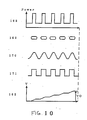
- Figure 10 shows the signal wave forms for the circuit of Figure 8 when the recording power is at the most suitable level.
- the recorded pits become as shown at 169.
- the wave form of the data read signal 170 then gives a digitised signal 171.
- the duty ratio of the signal 171 is 50%, and it will be understood that the recording power is now at the most suitable level.
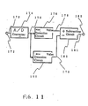
- FIG 11 is a circuit diagram of an alternative form of the recording state detection means 103 comprising amplitude measurement means.
- a data read signal 173 input from a terminal 172 is supplied to an A/D converter 174 and converted to a digital signal 175.
- the maximum value of the digital signal 175 is detected by a maximum value detection circuit 176 for generating a corresponding output 178, and the minimum value of the digital signal is detected by a minimum value detection circuit 177 for generating a corresponding output 179.
- amplitude data 181 is provided to a terminal 182 by subtracting the minimum value output 179 from the maximum value output 178 using a subtraction circuit 180.
- FIG 12 is a circuit diagram of another example of the amplitude measurement means.
- a data read signal 186 is input from a terminal 185 to an amplifier 187, which supplies an output signal 188 of the same phase as the signal 186 and an output signal 189 of the opposite phase from the signal 186. Further, the direct current biases of the outputs 188 and 189 are of the same potential.
- Full-wave rectification is carried out by transistors 190 and 191 and resistors 192 and 193.
- a condenser 194 is installed in order to smooth the signal after rectification.
- a buffer comprising an Op amp 195 then supplies an output signal 196 from a terminal 197, which represents the amplitude of the signal 186.
- FIG. 13 is a circuit diagram of an example of the optical output control means 104 and the optical source drive means 105.
- the optical output control means 104 will be explained first. Control of the optical output is carried out by a CPU 200.
- the CPU 200 has a one chip structure containing a ROM 203 and a RAM 204.
- the control program and constants are stored in the ROM 203, and the various measurement values and set values are stored in the RAM 204 to be used as necessary.
- a signal 202 representing the recording state of the pits is supplied from the recording state detection means 103 to a terminal 201.
- the CPU 200 supplies digital data 205 corresponding to the recording state to a D/A converter 206 for controlling recording power to set the pulse drive current of the semi-conductor laser at recording time.
- the optical source drive means 105 which generates a drive current for driving a semi-conductor laser 225, will now be explained.
- Current I LD flowing in the semi-conductor laser 225 comprises the sum of a bias current 229 (Ib) and a pulse current 228 (Ip).
- the bias current control circuit will be described first.
- the optical output of the semi-conductor laser 225 is detected by a monitoring photo-diode 226.
- a bias current control circuit 228 controls the current Ib so that the value of a monitor signal 227 is constant.
- the current Ib is held at its value immediately before recording by a control signal 231 input from a terminal 230.
- a constant current source which determines the pulse current Ip, comprises resistors 209 and 210, a transistor 211 and an Op amp 208.
- the current value is determined by an output signal 207 of the D/A converter 206 of the optical output control means 104.
- Transistors 217 and 218 switch the said current, and resistors 212, 213, 214, 215 and 216 impart biases to the transistors 217 and 218.
- Recording pulse data 222 is input from a terminal 221.
- An open collector type buffer 219 (a TTL 74LS07), and an open collector type inverter 220 (a TTL 74LS06) are also provided.
- the recording pulse data 222 is "L”
- the transistor 218 is on, the transistor 217 is off and the pulse current Ip flows to a resistor 223 without flowing to the semi-conductor laser 225.
- the recording pulse data 222 is "H”
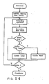
- Figure 14 is a flow chart showing the operation of the optical output control means 104 in Figure 13.
- the control process based on this Figure comprises the following steps:
- Figure 15 is a circuit diagram corresponding to Figure 13 but showing a modified form of the optical output control means 104.
- the circuit includes means for controlling the recording power and recording pulse width at the time of information recording.
- the same numbers are shown for the same elements as those appearing in Figure 13.
- the current drive circuit for the semi-conductor laser of the optical source control means 105 is identical to that shown in Figure 13 and, since it has been explained above, a further description will be omitted here.
- the optical output control means 104 only will be explained.
- the CPU 200 is a one chip structure containing the ROM 203 and the RAM 204.
- the control program and constants are stored in the ROM 203, and each measurement value and data for recording power and recording pulse width settings are stored in the RAM 204 for use as necessary.
- the CPU 200 transmits digital data 205 for controlling the recording power to the D/A converter 206, and sets the pulse current Ip, which drives the semi-conductor laser at the time of recording as above.
- a mono-stable multi-vibrator 240 using a TTL 74LS123 generates a recording pulse 241 of fixed duration T in response to the leading edge of pulses of the recording pulse data 222 input from the terminal 221.
- the resistance value of a resistor 242 is taken as R
- the capacitance of a condenser 243 is taken as C0
- the capacitance of a condenser 241 is taken as C1
- the capacitance of a condenser 245 is taken as C2.
- Transistors 246 and 247 serve as switches for controlling combinations of the capacitances C0, C1 and C2. Resistors 248 and 249 impart transistor bias currents. When a control signal 250 output from the CPU 200 becomes “H”, the transistor 246 turns on. In the same manner, when a control signal 251 becomes “H”, the transistor 247 turns on.
- the CPU 200 changes the recording power and the recording pulse width according to the signal 202 representing the recording state supplied from the recording state detection means 103 to terminal 201 for maintaining the optimum recording state.
- Figure 16 shows the sector format of an optical recording disk.
- the format has 1360 bytes per sector.
- the first five bytes constitute sector marks SM indicating the beginning of the sector.
- the next forty seven bytes are for ID, being the region where the track address and sector address are written. These five and forty seven bytes are pre-recorded as "pre-pits".
- the next fourteen bytes constitute the region called ODF flag and gaps.
- the last two bytes of this region designated 255 constitute the region called ALPC, which is furnished for calibration of the optical output of the semi-conductor laser, and can be used freely without stipulation as to use.
- the optical recording apparatus of the present invention may drive the semi-conductor laser to generate recording pulses of a specified pattern in the said ALPC region, detect the recording state from the data read signals of these pits recorded, and control the optical output of the semi-conductor laser so as to produce the optimum recording state.
- the recording state detection means 103 together with recording pulse formation means in this instance are shown in Figure 17.
- a pre-pit or start signal 257 is received at a terminal 256 and is input to a sector mark detection circuit 258, and a sector mark is detected and a corresponding signal 259 is output.
- a timing generation circuit 260 generates an ALPC timing signal 261 based on the sector mark signal 259.
- an MO signal 263 is input to a bistable circuit 264, to produce digital data 265.
- a duty detection circuit 266 measures the duty ratio of the digital data 265 while the ALPC timing signal 261 is active, and outputs a recording state detection signal 267 to a terminal 268.
- a recording clock signal 270 from a terminal 269 is input to a recording pulse generation circuit 271. While the ALPC timing signal 261 is active, the recording pulse generation circuit 271 generates a recording pulse 272 for output to a terminal 273.
- Figure 18 shows the signal wave forms for each part of the circuit of Figure 17.
- the ALPC timing signal 261 becomes active in the ALPC two-byte region except for two bits at each of the front and back portions of the region. This is for precision in the timing generation circuit and for absorbing disk rotation unevenness.
- the pattern of the recording data 274 repeats 010 in a shortest repetitive pattern of 2-7 modulation data, which results in the recording pulse 272 as shown.
- the duty ratio of the digital data 265, which is a digital representation of the data read signal 263 based on recorded pits 275, is 50% and corresponds with the optimum recording state. In this example, the pits are recorded in fours.
- Figure 19 shows a format diagram of the user data region of an optical recording disk.
- the leading twelve bytes designated 276 are an ID region called VFO3.
- the channel bit pattern of VFO3 is the shortest repetitive pattern 010010010010010010 ... 010010.
- the recording power of the semi-conductor laser is controlled so that the duty ratio is 50%.
- Recording pattern is shown in Figure 19.
- Such recording pattern composed of identification field and data field.
- the indentification field has VFO3 including twelve bytes such as the repetition of 010010 ... and SYNC pattern 3B, continuously. Actual data is written in the data field, successively.
- the length of a bit is unitary, it is possible to measure the duration of a pulse based on a bit not only in the VFO3 region but anywhere in the user zone, employing a pit position detection method.
- a pit edge recording method either a part or all of the pit length can be measured relative to the VFO3 pattern where the duration is pre-determined.
- the present invention as described above has the effect of allowing recording to be controlled so that the recording power is constantly at an optimum consistent with variation in recording sensitivity as a result of disk temperature changes and ageing.
- the apparatus is advantageous from the stand point of disk inter-changeability because optimisation of the recording power is performed automatically by the apparatus for disks of different recording sensitivies.
Landscapes
- Physics & Mathematics (AREA)
- Optics & Photonics (AREA)
- Optical Recording Or Reproduction (AREA)
Applications Claiming Priority (2)
| Application Number | Priority Date | Filing Date | Title |
|---|---|---|---|
| JP94621/90 | 1990-04-10 | ||
| JP9462190A JP2910143B2 (ja) | 1989-08-28 | 1990-04-10 | 光学式記録再生装置 |
Publications (2)
| Publication Number | Publication Date |
|---|---|
| EP0453161A2 true EP0453161A2 (fr) | 1991-10-23 |
| EP0453161A3 EP0453161A3 (en) | 1992-07-08 |
Family
ID=14115329
Family Applications (1)
| Application Number | Title | Priority Date | Filing Date |
|---|---|---|---|
| EP19910303148 Withdrawn EP0453161A3 (en) | 1990-04-10 | 1991-04-10 | Optical recording apparatus |
Country Status (1)
| Country | Link |
|---|---|
| EP (1) | EP0453161A3 (fr) |
Cited By (5)
| Publication number | Priority date | Publication date | Assignee | Title |
|---|---|---|---|---|
| EP0544276A3 (en) * | 1991-11-25 | 1993-12-08 | Sony Corp | Writable optical disk recording apparatus |
| US5490127A (en) * | 1993-05-11 | 1996-02-06 | Sony Corporation | Asymmetry detector for use in an optical recording and reproducing device |
| EP0684599A3 (fr) * | 1994-05-26 | 1996-07-31 | Ibm | ContrÔle et réglage de la puissance laser d'éniture dans un enregistreur de données optique. |
| US5970026A (en) * | 1990-07-11 | 1999-10-19 | Sony Corporation | Temperature invariant, magneto-optic modulator coil driving circuit |
| WO2005057564A1 (fr) * | 2003-12-09 | 2005-06-23 | Koninklijke Philips Electronics N.V. | Procede et appareil permettant l'inscription sur disques optiques avec etalonnage de puissance optimise |
Family Cites Families (6)
| Publication number | Priority date | Publication date | Assignee | Title |
|---|---|---|---|---|
| JPS54143109A (en) * | 1978-04-28 | 1979-11-08 | Hitachi Ltd | Optical information device |
| JPS5668935A (en) * | 1979-10-22 | 1981-06-09 | Discovision Ass | Device for recording dataasignal on movable optical recording medium |
| US4358774A (en) * | 1980-07-14 | 1982-11-09 | Discovision Associates | Apparatus and method for controlling focus in a recording system |
| FR2546325B1 (fr) * | 1983-05-20 | 1988-07-08 | Thomson Csf | Procede et dispositif de calibration de la puissance optique appliquee a un disque optique pour l'enregistrement de donnees |
| EP0289004B1 (fr) * | 1987-04-28 | 1994-03-23 | Sharp Kabushiki Kaisha | Appareil d'enregistrement et de reproduction |
| ATE114856T1 (de) * | 1989-06-23 | 1994-12-15 | Philips Nv | Aufzeichnungsanordnung zum anbringen eines informationsmusters auf einem strahlungsempfindlichen aufzeichnungsträger. |
-
1991
- 1991-04-10 EP EP19910303148 patent/EP0453161A3/en not_active Withdrawn
Cited By (6)
| Publication number | Priority date | Publication date | Assignee | Title |
|---|---|---|---|---|
| US5970026A (en) * | 1990-07-11 | 1999-10-19 | Sony Corporation | Temperature invariant, magneto-optic modulator coil driving circuit |
| EP0544276A3 (en) * | 1991-11-25 | 1993-12-08 | Sony Corp | Writable optical disk recording apparatus |
| US5353270A (en) * | 1991-11-25 | 1994-10-04 | Sony Corporation | Writable optical disk recording apparatus |
| US5490127A (en) * | 1993-05-11 | 1996-02-06 | Sony Corporation | Asymmetry detector for use in an optical recording and reproducing device |
| EP0684599A3 (fr) * | 1994-05-26 | 1996-07-31 | Ibm | ContrÔle et réglage de la puissance laser d'éniture dans un enregistreur de données optique. |
| WO2005057564A1 (fr) * | 2003-12-09 | 2005-06-23 | Koninklijke Philips Electronics N.V. | Procede et appareil permettant l'inscription sur disques optiques avec etalonnage de puissance optimise |
Also Published As
| Publication number | Publication date |
|---|---|
| EP0453161A3 (en) | 1992-07-08 |
Similar Documents
| Publication | Publication Date | Title |
|---|---|---|
| US5629921A (en) | Level detector for detecting a voltage level of a signal | |
| CA1277766C (fr) | Methode et appareil d'enregistrement et de lecture optiques | |
| US6269062B1 (en) | Arrangements for using detected phase differences for setting laser power levels | |
| US4788674A (en) | Optical disc record reproducing apparatus | |
| US7009923B2 (en) | Method of and apparatus for recording information | |
| US7242653B2 (en) | Optical disc apparatus capable of detecting recording characteristics based on a predetermined signal prerecorded and reproduced | |
| US6577571B2 (en) | Optical disk recording apparatus and method of recording data on optical disk | |
| BR9917693B1 (pt) | Circuito de escrita adaptativo para escrita de dado de entrada em um mecanismo de registro ótico, e circuito de geração de pulso de escrita adaptativo | |
| KR100679169B1 (ko) | 광 디스크 기록장치 및 광 디스크 기록매체 | |
| JPS61216141A (ja) | 光学式記録再生装置における半導体レーザ劣化判別装置 | |
| US5798992A (en) | Laser diode monitoring apparatus for determining the decay of laser diode | |
| EP0453161A2 (fr) | Appareil d'enregistrement optique | |
| US6487152B1 (en) | Method of recording information in phase-change recording medium and recording medium for use in the method | |
| US20030156515A1 (en) | Methods of determining the optimal erase and write power, and recording apparatus with devices for said methods | |
| US5493549A (en) | Optical recording regeneration apparatus with compensation circuit | |
| EP0621589B1 (fr) | Méthode pour obtenir un signal "qualité" d'un signal lu, ainsi qu'un dispositif d'enregistrement et un dispositif de lecture utilisant une telle méthode | |
| JPH04149824A (ja) | 光ディスクの情報読取装置 | |
| US7522509B2 (en) | Semiconductor laser driving device and optical disc device | |
| US7126896B2 (en) | Information recording method, recording condition detection method, and information recording apparatus | |
| KR100498474B1 (ko) | 레이저 파워 모니터 장치와 그를 포함하는 광픽업 장치 및광 기록 재생 기기 | |
| JP3518186B2 (ja) | 試し書き方法及びそれを用いた情報記録再生装置 | |
| KR19990016023A (ko) | 레이저 다이오드 광출력 제어방법 및 장치 | |
| JP2910143B2 (ja) | 光学式記録再生装置 | |
| JP3259640B2 (ja) | 最適記録パワー検出方法 | |
| US5719838A (en) | β compensation using a defocus technique |
Legal Events
| Date | Code | Title | Description |
|---|---|---|---|
| PUAI | Public reference made under article 153(3) epc to a published international application that has entered the european phase |
Free format text: ORIGINAL CODE: 0009012 |
|
| AK | Designated contracting states |
Kind code of ref document: A2 Designated state(s): DE FR GB NL |
|
| PUAL | Search report despatched |
Free format text: ORIGINAL CODE: 0009013 |
|
| AK | Designated contracting states |
Kind code of ref document: A3 Designated state(s): DE FR GB NL |
|
| 17P | Request for examination filed |
Effective date: 19921230 |
|
| 17Q | First examination report despatched |
Effective date: 19940720 |
|
| STAA | Information on the status of an ep patent application or granted ep patent |
Free format text: STATUS: THE APPLICATION IS DEEMED TO BE WITHDRAWN |
|
| 18D | Application deemed to be withdrawn |
Effective date: 19980707 |