EP0453814A2 - Système adaptatif d'estimation de réponses impulsionnelles de canal au moyen d'estimation de séquence ayant un maximum de vraisemblance - Google Patents
Système adaptatif d'estimation de réponses impulsionnelles de canal au moyen d'estimation de séquence ayant un maximum de vraisemblance Download PDFInfo
- Publication number
- EP0453814A2 EP0453814A2 EP91105002A EP91105002A EP0453814A2 EP 0453814 A2 EP0453814 A2 EP 0453814A2 EP 91105002 A EP91105002 A EP 91105002A EP 91105002 A EP91105002 A EP 91105002A EP 0453814 A2 EP0453814 A2 EP 0453814A2
- Authority
- EP
- European Patent Office
- Prior art keywords
- output
- circuit
- outputting
- received signal
- switch
- Prior art date
- Legal status (The legal status is an assumption and is not a legal conclusion. Google has not performed a legal analysis and makes no representation as to the accuracy of the status listed.)
- Granted
Links
Images


Classifications
-
- H—ELECTRICITY
- H04—ELECTRIC COMMUNICATION TECHNIQUE
- H04L—TRANSMISSION OF DIGITAL INFORMATION, e.g. TELEGRAPHIC COMMUNICATION
- H04L25/00—Baseband systems
- H04L25/02—Details ; arrangements for supplying electrical power along data transmission lines
- H04L25/03—Shaping networks in transmitter or receiver, e.g. adaptive shaping networks
- H04L25/03006—Arrangements for removing intersymbol interference
- H04L25/03178—Arrangements involving sequence estimation techniques
- H04L25/03337—Arrangements involving per-survivor processing
-
- H—ELECTRICITY
- H04—ELECTRIC COMMUNICATION TECHNIQUE
- H04L—TRANSMISSION OF DIGITAL INFORMATION, e.g. TELEGRAPHIC COMMUNICATION
- H04L25/00—Baseband systems
- H04L25/02—Details ; arrangements for supplying electrical power along data transmission lines
- H04L25/03—Shaping networks in transmitter or receiver, e.g. adaptive shaping networks
- H04L25/03006—Arrangements for removing intersymbol interference
- H04L25/03178—Arrangements involving sequence estimation techniques
- H04L25/03248—Arrangements for operating in conjunction with other apparatus
- H04L25/03292—Arrangements for operating in conjunction with other apparatus with channel estimation circuitry
Definitions
- the present invention relates to a digital data communication system and, more particularly, to an adaptive channel impulse response estimation system for estimating an impulse response reliably at the receiving side of a channel which varies with time and suffers from distortions due to intersymbol intereference and an adaptive maximum likelihood sequence estimation (MLSE) system for demodulating received data correctly by reducing the influence of demodulation delay.
- an adaptive channel impulse response estimation system for estimating an impulse response reliably at the receiving side of a channel which varies with time and suffers from distortions due to intersymbol intereference
- an adaptive maximum likelihood sequence estimation (MLSE) system for demodulating received data correctly by reducing the influence of demodulation delay.
- the receiving side needs an adaptive equalizer adapting itself to the characteristic of the channel to demodulate received data correctly. If the impulse response of the channel is known, the adaptive equalizer can be constructed to satisfy a predetermined characteistic. It is therefore necessary to estimate the impulse response of the time-varying channel from a received signal, so that the equalizer may follow the channel.
- a conventional implementation for estimating a channel impulse response from a received signal consists in applying the output of a decision unit to a replica generating filter which generates a replica of a received signal and is implemented as a transversal filter, comparing the replica with the actual received signal, and controlling the tap coefficients of the filter in such a manner as to reduce a difference therebetween, as disclosed in, for example, Proakis "Digital Communications", McGraw-Hill, 1983 (referred to as PRIOR ART I hereinafter).
- the tap coefficients of the replica generating filter are outputted as an estimated channel impulse response, and an adaptive equalizer is controlled in matching relation to the estimated channel impulse response.
- estimating a channel impulse response from a decision result is disadvanageous in that a decision error would cause the replica generating filter to diverge and thereby render the operation of the adaptive equalizer itself unstable, resulting in error propagation.
- the adaptive equation system may be implemented by MLSE using Viterbi algorithm, as taught in, for example, Hayes "The Viterbi Algorithm Applied to Digital Data Transmission", IEEE, Communication Society, 1975, No. 13 (hereinafter referred to as PRIOR ART II).
- This scheme successfully reduces decision errors and, therefore, stabilizes the operation of the replica generating filter so long as the channel varies slowly.
- the ability of the filter to follow the channel variation is degraded due to demodulation delay particular to the MLSE scheme with the result that the decision error is aggravated.
- an MLSE system for a digital data communication system which transmits data over a transmission channel comprises a circuit for estimating an MLS on the basis of a received signal and a predicted future channel impulse response applied thereto, and outputting the result of estimation, a circuit for generating a replica of the received signal on the basis of the result of estimation and internal states thereof, producing a difference between the received signal and the replica, changing the internal states in a direction for reducing the difference, and outputting the result of change, and a circuit for predicting a future channel impulse response on the basis of the result of change applied thereto by using the result of change as a past change in internal states, and outputting the result of prediction.
- an adaptive MLSE apparatus using Viterbi algorithm and applicable to a digital data communication system which transmits data over a transmission channel comprises a matched filter to which a received signal and a predicted future channel impulse response are applied, a branchmetric compute circuit for calculating, in response to the predicted future channel impulse response and an output of the matched filter, a branchmetric of the received signal and outputting the branchmetric, an add, compare and select (ACS) circuit for estimating an MLS in response to an output of the branchmetric compute circuit, and outputting the result of estimation, a delay circuit for delaying the received signal by a demodulation time in which the result of estimation is outputted, a received signal regenerating filter for regenerating and outputting the received signal in response to an output of the ACS circuit, a filter control circuit for updating, in response to an output of the delay circuit, an output of the received signal regenerating filter, and internal states of the received signal regenerating filter, the internal states of the received signal regenerating filter such that a difference
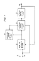
- the system has input terminals 12 and 14, a replica generating filter 16 for generating a replica of a received signal, an internal state convert circuit 18, a decision error detect circuit 20, an internal state update circuit 22, and an output terminal 24.
- a signal representative of the result of decision is applied via the input terminal 12 to the replica generating filter 16.
- the received signal is applied via the input terminal 14 to the replica generating filter 16 and internal state convert circuit 18.
- the filter 16 may be implemented as a 3-tap transversal filter having an input terminal 32 which is supplied with the signal of the result of decision and an input terminal 34 which is supplied with the received signal, shift registers 36, 38 and 40, tap coefficient memories 42, 44 and 46, multipliers 48, 50 and 52, an adder 54, a subtractor 56, output terminals 58, 60, 62 and 64, and input/output terminal 66, 68 and 70.
- the tap coefficients of the transversal filter 16, i.e., the outputs appearing on the input/output terminals 66, 68 and 70 are the estimated values of channel impulse response.
- the tap coefficients, signals stored in the registers 36, 38 and 40, i.e., outputs appearing on the output terminals 60, 62 and 64, and an error signal, i.e., output appearing on the output terminal 58 define the internal states of the filter 16.
- the replica generating filter 16 outputs the current internal state thereof to the internal state convert circuit and decision error detect circuit 20.
- the decision error detect circuit 20 determines whether or not a decision error has occurred on the basis of the internal states. On determining that a decision error has occurred, the detecting circuit 20 feeds a start control pulse to the internal state convert circuit 18.
- the convert circuit 18 converts the internal states on the basis of the received signal from the input terminal 14 and the internal states of the filter 16 in such a manner as to eliminate error propagation. The result of conversion is applied to the internal state update circuit 22.
- the update circuit 22 feeds updated values of tap coefficients to the filter 16 while feeding the estimated channel impulse response values, i.e., updated tap coefficients to the output terminal 24.
- FIG. 3 An alternative embodiment of the present invention is shown in Fig. 3 and implemented by applying the adaptive channel impulse response estimation system to the MLSE system.
- the system has an input terminal 82, an MLSE circuit 84, a replica generating filter 86, an error propagation suppress circuit 88, a comparator 90, a tap coefficient updatae circuit 92, and an output terminal 94.
- the replica generating filter 86, error propagation suppress circuit 88, comparator 90 and tap coefficient update circuit 92 constitute the gist of this embodiment.
- the filter 86 may also be implemented as a 3-tap transversal filter, as shown in Fig. 2.
- a received signal arrived at the input terminal 82 is applied to the MLSE circuit 84, replica generating filter 86, and error propagation suppress circuit 88.
- the MLSE circuit 84 involves demodulation delay, it is necessary to delay the received signal by the demodulation delay before feeding it to the filter 86 and suppress circuit 88.
- the demodulation delay in the MLSE circuit 84 be assumed to be zero.
- the MLSE circuit 84 executes MLSE with the received signal and applies the result of estimation to the output terminal 94 and filter 86.
- the filter 86 produces a signal representative of a difference between the received signal come in through the input terminal 82 and a received signal replica which the filter 86 generates.
- the internal states (decision pattern) of the shift registers 36, 38 and 40 appearing on the output terminals 60, 62 and 64, Fig. 2, tap coefficients appearing on the input/output terminals 66, 68 and 70, Fig. 2, and the error signal appearing on the output terminal 58, Fig. 2 are representative of the internal states of the filter 86.
- the filter 86 delivers such an internal states to the error propagation suppress circuit 88 and comparator 90.
- the comparator 90 detects, among the input internal states, the level of the error signal and compares it with a predetermined threshold level which exceeds, for example, a decision range.
- the comparator 90 feeds a start control pulse to the error propagation suppress circuit 88 determining that a decision error has occurred.
- the suppress circuit 88 converts the internal states from the filter 86 in such a manner as to suppress error propagation and then outputs the result of conversion.
- Fig. 4 shows a specific construction of the error propagation suppress circuit 88.
- the construction of Fig. 4 is applicable to a case wherein the filter 86 has three taps as shown in Fig. 2, i.e., the number n of shift registers is "3" while the number n of signals in each shift register is "1". Generally, the construction is extendible even when n and m each has any other value. In Fig.
- the internal states from the filter 86 are applied to the input terminals 100, 102, 104, 106, 108, 110 and 112. Specifically, signals on the output terminals 60, 62 and 64, Fig. 2, are respectively applied to the input terminals 100, 102 and 104, signals on the output terminals 66, 68 and 70, Fig. 2, are respectively applied to the input terminals 106, 108 and 110, and the signal on the output terminal 58, Fig. 2, is applied to the input terminal 112. Applied to the input terminals 114 and 116 are the control pulse from the comparator 90 and the received signal, respectively. On receiving the control pulse via the input terminal 114, the control circuit 118 delivers a start control signal to the decision result pattern generate circuit 120.
- the control circuit 118 feeds control signals to the switches 150 and 154 and thereby causes them to deliver input signals to, respectively, the switches 148 and 156 as initial states.
- the control circuit 118 causes the switches 150 and 154 to deliver input signals to the switches 152 and 159, respectively. Further, the control circuit 118 applies control signals to the switches 152 and 159 to cause them to output the signals from the switches 150 and 154, respectively.
- the switches 152 and 159 outputs respectively the signals from the input terminals 112 and 100 when not supplied with the control signals from the control circuit 118.
- the decision pattern generate circuit 120 In response to the control signal from the control circuit 118, the decision pattern generate circuit 120 generates all of m T possible decision patterns. In the embodiment, m is assumed to be "1".
- the decision patterns are fed from the decision pattern generate section 120 to the multiplier 132.
- the internal states of the filter 86 are stored in the memories 128 and 130.
- the multipliers 132, 134 and 136 and adder 138 weight the signals stored in the memories 128 and 130 and the signal from the decision pattern generate circuit 120 by the signals stored in the tap coefficients memories 122, 124 and 126 and then add the weighted signals.
- the subtractor 140 produces a signal representative of a difference between the output of the adder 138 and the received signal come in through the input terminal 114.
- This output of the subtractor 140 is fed to the power detect circuit 142 and switch 148.
- the switch 148 is so set as to select the output of the subtractor 140 and apply it to the memory 158.
- the memory 158 usually delivers the content thereof to the switch 150 and power detect circuit 144.
- the power detect circuit 144 detects the power of the input signal and feeds it to the comparator 146.
- the comparator 146 selects smaller one of the outputs of the power detecting circuits 142 and 144.
- the comparator 146 controls the switch 148 such that if the output of the power detect circuit 144 is smaller than that of the power detect circuit 142, the output of the switch 150 is fed to the memory 158 or, if otherwise, the output of the subtractor 140 is fed to the memory 158.
- the memory 58 stores an error signal minimizing the power at all times.
- the comparator 146 controls the switch 156 such that if the output of the power detect circuit 142 is smaller than that of the power detect circuit 144, the output of the decision pattern generate circuit 120 is fed to the memory 160 or, if otherwise, the output of the switch 154 is fed to the memory 60.
- the switch 156 is so set as to select the output of the decision pattern generate circuit 120.
- the memory 160 always stores a decision pattern which provides the minimum error signal power.
- the internal states undergone conversion as stated above are transferred to the tap coefficient update circuit 92.
- the filter 86 and the error propagation suppress circuit 88 have the specific constructions shown in Figs. 2 and 4, respectively.
- the tap coefficients of the filter 86 applied to the output terminals 162, 164 and 166, Fig. 4 are the estimated values of the path impulse response at a time K-1.
- the update circuit 92 determines tap coefficients at a time k by using the converted internal states and algorithm such as LMS algorithm taught in the previously stated PRIOR ART I. Such tap coefficients are applied to the MLSE circuit 84 and filter 86.
- the MLSE circuit 84 and filter 86 each continues adaptive oeprations while updating the internal states thereof in response to the output of the update circuit 92.
- the system has an input terminal 182, an MLSE circuit 184, a received signal regenerating filter 186, a channel impulse response predict circuit 188, and an output terminal 190.
- a received signal is applied to the MLSE circuit 184 and received signal regenerating filter 186 via the input terminal 182.
- the MLSE circuit 184 executes MLSE with the received signal and feeds the result of estimation to the outptut 190 and filter 186.
- the filter 186 generates a replica of the received signal on the basis of the result of estimation and the internal states thereof.
- the filter 186 compares the received signal come in through the input terminal 182 and the replica and updates the internal states thereof in such a manner as to reduce their difference or error.
- the updated states of the filter 186 are fed to the channel impulse response predict circuit 188.
- the predict circuit 188 predicts a future channel impulse response and delivers the result of prediction to the MLSE circuit 184.
- the MLSE circuit 184 changes the internal states thereof in matching relation to the future channel impulse response.
- Fig. 6 shows a fourth embodiment of the present invention which is concerned with the adaptive MLSE system.
- an input terminal 202 a matched filter 204, a branchmetric compute circuit 206, an add, compare and select (ACS) circuit 208, a delay circuit 210, a received signal regenerating filter 212, a channel impulse response predict circuit 214, an output terminal 216, and a filter control circuit 218.
- the matched filter 202, sayhmetric compute circuit 206 and ACS circuit 208 constitute in combination an MLSE circuit using Viterbi algorithm.
- the matched filter 204 and branchmetric compute circuit 206 each has dependency on channel impulse response (see PRIOR ART II).
- the received signal from the input terminal 202 is applied to the MLSE circuit constituted by the matched filter 204, branchmetric compute circuit 206, and ACS circuit 208, and to the delay circuit 210.
- the ACS circuit 208 delivers the MLSE result to the regenerating filter 212.
- the replica of the received signal and the internal states of the regenerating filter 212 are applied to the filter control circuit 218.
- Also applied to the filter control circuit 218 is the received signal having been delayed by an MLSE modulation time by the delay circuit 210. Assuming that the channel impulse response has a length of "3", then the filter 212 and filter control circuit 218 may be implemented as a transversal filter and a processor, as shown in Fig. 7.
- Fig. 7 there are shown input terminals 222 and 224, shift registers 226 and 228, multipliers 230, 232 and 234, an adder 236, a subtractor 238, a processor 240, circuits 242, 244 and 246 for generating channel impulse response values ⁇ o (k), ⁇ 1(k) and ⁇ 2(k), respectively, and output terminals 248, 250 and 252.
- the estimated channel impulse response values 242, 244 and 246 and the contents of the shift registers 226 and 228 are the internal states of the regenerating filter 212.
- the result of decision a (k) from the ACS circuit 208 is applied to the input terminal 222.
- the multipliers 230, 232 and 234 multiply the results of decision a (k-2) to a (k) by the channel impulse response values ⁇ 0(k) to ⁇ 2(k) estimated at the time k , while the adder 236 adds the resulted products. As a result, a replica of the k th received signal r(k) appears on the output of the adder 236. On the other hand, a received signal r(k) delayed by the delay circuit 210 arrives at the input terminal 224. The subtractor 238 produces a difference or error ⁇ ( ⁇ (k)) between the received signal r (k) and the output of the adder 236 and delivers it to a processor 240.
- the processor 240 updates the channel impulse response vaues ⁇ 0(k) to ⁇ 2(k) such that the square mean, for example, of the error ⁇ ( ⁇ (k)) becomes minimum.
- the processor 240 updates ⁇ 0(k) to ⁇ 2(k) by the following calculations: where ⁇ is the step size and * is the complex conjugate.
- the processor 240 delivers resulted ⁇ 0(k + 1), ⁇ 1(k + 1) and ⁇ 2(k + 1) to the circuits 242, 244 and 246, respectively, and to the output terminals 248, 250 and 252 as an estimated impulse response.
- the received signal regenerating filter 212 can estimate only the path impulse response delayed by the modulation delay of the MLSE circuit 184. To correct the delay, the output of the filter control circuit 218 is applied to the channel impulse response predict circuit 214.
- the channel impulse response predict circuit 214 may be constituted by a 3-tap transversal filter and a processor.
- the arrangement shown in Fig. 8 has an input terminal 262, shift registers 264, 266, 268, 270, 272 and 274, multipliers 276, 278 and 280, an adder 282, a subtractor 284, tap coefficient circuits 286, 288 and 290, a processor 292, and an output terminal 294.
- the shift registers 264, 266 and 268 store past estimated channel impulse response values ⁇ i (k - 1), ⁇ i (k - 2) and ⁇ i (k - 3), respectively.
- the multipliers 276, 278 and 280 multiply respectively such impulse response values ⁇ i (k - 1), ⁇ i (k - 2) and ⁇ i (k - 3) by the tap coefficients of the tap coefficient circuits 286, 288 and 290, while the adder 282 adds the resulted products.
- the output of the adder 282 is fed to the output terminal 294 and shift register 270 as a predicted path impulse response value ⁇ i (k + 3) 3T ahead.
- the shift registers 270, 272 and 274 shift the contents thereof, i.e., the past predicted channel impulse response values ⁇ i (k + 2), ⁇ i (k + 1) and ⁇ i (k).
- the subtractor 284 produces a difference or error ⁇ ( i (k)) between the output ⁇ i of the shift register 274 and the predicted past impulse response value ⁇ i (k) fed from the input terminal 262 and feeds it to the processor 292.
- the processor 292 updates tap coefficients P0(k) P1(k) and P2(k) by using an adaptation algorithm such that the square mean, for example, of the error ⁇ (h i (k)) becomes smallest. Assuming that use is made of MLS algorithm as the adaptation algorithm, the processor 292 updates the above-mentioned tap coefficients, as follows: where ⁇ is the step size and * is the complex conjugate.
- the illustrative embodiment predicts the current channel impulse response on the basis of the past estimated channel impulse response and causes the matched filter 204 and branchmetric compute circuit 206 to change adaptively by using the predicted value. This is successful in reducing the influence of demodulation delay particular to the MLSE system and, therefore, in realizing highly reliable demodulation.
- the present invention provides a digital data communication system which estimates a channel impulse response reliably even when the transmission channel is time-varying and suffers from intersymbol interference.
- the influence of demodulation delay occurring in an MLSE estimator is reduced to implement highly reliable data transmission.
Landscapes
- Engineering & Computer Science (AREA)
- Physics & Mathematics (AREA)
- Optics & Photonics (AREA)
- Power Engineering (AREA)
- Computer Networks & Wireless Communication (AREA)
- Signal Processing (AREA)
- Cable Transmission Systems, Equalization Of Radio And Reduction Of Echo (AREA)
- Filters That Use Time-Delay Elements (AREA)
- Dc Digital Transmission (AREA)
Applications Claiming Priority (4)
| Application Number | Priority Date | Filing Date | Title |
|---|---|---|---|
| JP85640/90 | 1990-03-30 | ||
| JP85638/90 | 1990-03-30 | ||
| JP8563890A JPH03284013A (ja) | 1990-03-30 | 1990-03-30 | 適応型最尤系列推定方式及び装置 |
| JP2085640A JP2546022B2 (ja) | 1990-03-30 | 1990-03-30 | 適応型通信路インパルスレスポンス推定方式 |
Publications (3)
| Publication Number | Publication Date |
|---|---|
| EP0453814A2 true EP0453814A2 (fr) | 1991-10-30 |
| EP0453814A3 EP0453814A3 (en) | 1992-09-23 |
| EP0453814B1 EP0453814B1 (fr) | 1997-01-29 |
Family
ID=26426647
Family Applications (1)
| Application Number | Title | Priority Date | Filing Date |
|---|---|---|---|
| EP91105002A Expired - Lifetime EP0453814B1 (fr) | 1990-03-30 | 1991-03-28 | Système adaptatif d'estimation de réponses impulsionnelles de canal au moyen d'estimation de séquence ayant un maximum de vraisemblance |
Country Status (4)
| Country | Link |
|---|---|
| US (1) | US5224127A (fr) |
| EP (1) | EP0453814B1 (fr) |
| CA (1) | CA2039373C (fr) |
| DE (1) | DE69124413T2 (fr) |
Cited By (11)
| Publication number | Priority date | Publication date | Assignee | Title |
|---|---|---|---|---|
| EP0508407A3 (en) * | 1991-04-08 | 1993-07-07 | Nippon Telegraph And Telephone Corporation | Maximum likelihood sequence estimation for rapidly varying mobile radio communication channels |
| DE4201810A1 (de) * | 1992-01-24 | 1993-07-29 | Aeg Mobile Communication | Digitales nachrichtenuebertragungssystem |
| EP0550143A3 (en) * | 1991-12-31 | 1993-09-29 | American Telephone And Telegraph Company | Mlse for mobile radio channels |
| DE4290581C2 (de) * | 1991-02-28 | 1994-05-05 | Motorola Inc | Signalwichtungssystem für einen Digitalempfänger |
| EP0660543A3 (fr) * | 1993-12-24 | 1996-12-18 | Nec Corp | Système et procédé adaptatif d'estimation de séquence à maximum de vraisemblance. |
| US5862192A (en) * | 1991-12-31 | 1999-01-19 | Lucent Technologies Inc. | Methods and apparatus for equalization and decoding of digital communications channels using antenna diversity |
| GB2335123A (en) * | 1998-03-07 | 1999-09-08 | Siemens Ag | Equaliser with adaptable channel impulse response estimation |
| RU2144739C1 (ru) * | 1994-09-14 | 2000-01-20 | Эрикссон Инк. | Способ демодулирования сигналов данных, модулированных цифровым способом |
| US6111923A (en) * | 1991-10-21 | 2000-08-29 | Motorola, Inc. | System and method for calculating a state transition metric in a viterbi equalizer |
| WO2001031866A3 (fr) * | 1999-10-25 | 2001-10-25 | Ericsson Inc | isaCESSEUR DE BANDE DE BASE A CAPACITES D'EVALUATION DE PARAMETRES ANTICIPEE |
| US7440489B2 (en) | 2001-08-07 | 2008-10-21 | Ericsson Inc. | Method and apparatus for selective demodulation and decoding of communications signals |
Families Citing this family (9)
| Publication number | Priority date | Publication date | Assignee | Title |
|---|---|---|---|---|
| JP2546022B2 (ja) | 1990-03-30 | 1996-10-23 | 日本電気株式会社 | 適応型通信路インパルスレスポンス推定方式 |
| DE4135953A1 (de) * | 1991-10-31 | 1993-05-06 | Rohde & Schwarz Gmbh & Co Kg, 8000 Muenchen, De | Verfahren zum bestimmen der komplexen impulsantwort eines funkkanals |
| US5615233A (en) * | 1992-07-22 | 1997-03-25 | Motorola, Inc. | Method for channel estimation using individual adaptation |
| US5615226A (en) * | 1995-02-27 | 1997-03-25 | Motorola, Inc. | Method and receiver for demodulating a received signal |
| JPH09294095A (ja) * | 1996-04-26 | 1997-11-11 | Oki Electric Ind Co Ltd | 適応等化器 |
| JPH1141115A (ja) * | 1997-07-23 | 1999-02-12 | Mitsubishi Electric Corp | ディジタルデータ復調装置 |
| JPH1188118A (ja) * | 1997-09-03 | 1999-03-30 | Matsushita Electric Ind Co Ltd | マッチトフィルタ及びタイミング検出方法 |
| FI104772B (fi) | 1998-03-23 | 2000-03-31 | Nokia Networks Oy | Itseoptimoiva kanavakorjaus- ja ilmaisumenetelmä ja itseoptimoiva kanavakorjain/ilmaisin |
| US6820227B2 (en) * | 2001-11-15 | 2004-11-16 | International Business Machines Corporation | Method and apparatus for performing error checking |
Family Cites Families (4)
| Publication number | Priority date | Publication date | Assignee | Title |
|---|---|---|---|---|
| JPS62233933A (ja) * | 1986-04-03 | 1987-10-14 | Toshiba Corp | ヴイタビ復号法 |
| GB8609711D0 (en) * | 1986-04-21 | 1986-05-29 | Clark A P | Channel estimation & detection |
| US4885757A (en) * | 1987-06-01 | 1989-12-05 | Texas Instruments Incorporated | Digital adaptive receiver employing maximum-likelihood sequence estimation with neural networks |
| JPH03195129A (ja) * | 1989-12-22 | 1991-08-26 | Mitsubishi Electric Corp | 最尤系列推定装置 |
-
1991
- 1991-03-28 DE DE69124413T patent/DE69124413T2/de not_active Expired - Lifetime
- 1991-03-28 EP EP91105002A patent/EP0453814B1/fr not_active Expired - Lifetime
- 1991-03-28 CA CA002039373A patent/CA2039373C/fr not_active Expired - Lifetime
- 1991-04-01 US US07/678,519 patent/US5224127A/en not_active Expired - Lifetime
Cited By (16)
| Publication number | Priority date | Publication date | Assignee | Title |
|---|---|---|---|---|
| DE4290581C2 (de) * | 1991-02-28 | 1994-05-05 | Motorola Inc | Signalwichtungssystem für einen Digitalempfänger |
| US5436928A (en) * | 1991-04-08 | 1995-07-25 | Nippon Telegraph And Telephone Corporation | Method and apparatus for equalizing transmission line characteristics which vary at high speed in mobile radio communication |
| EP0508407A3 (en) * | 1991-04-08 | 1993-07-07 | Nippon Telegraph And Telephone Corporation | Maximum likelihood sequence estimation for rapidly varying mobile radio communication channels |
| US6111923A (en) * | 1991-10-21 | 2000-08-29 | Motorola, Inc. | System and method for calculating a state transition metric in a viterbi equalizer |
| US5862156A (en) * | 1991-12-31 | 1999-01-19 | Lucent Technologies Inc. | Adaptive sequence estimation for digital cellular radio channels |
| US5862192A (en) * | 1991-12-31 | 1999-01-19 | Lucent Technologies Inc. | Methods and apparatus for equalization and decoding of digital communications channels using antenna diversity |
| EP0550143A3 (en) * | 1991-12-31 | 1993-09-29 | American Telephone And Telegraph Company | Mlse for mobile radio channels |
| DE4201810A1 (de) * | 1992-01-24 | 1993-07-29 | Aeg Mobile Communication | Digitales nachrichtenuebertragungssystem |
| EP0660543A3 (fr) * | 1993-12-24 | 1996-12-18 | Nec Corp | Système et procédé adaptatif d'estimation de séquence à maximum de vraisemblance. |
| US5673288A (en) * | 1993-12-24 | 1997-09-30 | Nec Corporation | System and method for adaptive maximum likelihood sequence estimation |
| RU2144739C1 (ru) * | 1994-09-14 | 2000-01-20 | Эрикссон Инк. | Способ демодулирования сигналов данных, модулированных цифровым способом |
| GB2335123A (en) * | 1998-03-07 | 1999-09-08 | Siemens Ag | Equaliser with adaptable channel impulse response estimation |
| GB2335123B (en) * | 1998-03-07 | 2003-08-13 | Siemens Ag | Communications receiver and method of detecting data from received signals |
| WO2001031866A3 (fr) * | 1999-10-25 | 2001-10-25 | Ericsson Inc | isaCESSEUR DE BANDE DE BASE A CAPACITES D'EVALUATION DE PARAMETRES ANTICIPEE |
| US6570910B1 (en) | 1999-10-25 | 2003-05-27 | Ericsson Inc. | Baseband processor with look-ahead parameter estimation capabilities |
| US7440489B2 (en) | 2001-08-07 | 2008-10-21 | Ericsson Inc. | Method and apparatus for selective demodulation and decoding of communications signals |
Also Published As
| Publication number | Publication date |
|---|---|
| CA2039373C (fr) | 1996-09-10 |
| DE69124413T2 (de) | 1997-06-05 |
| CA2039373A1 (fr) | 1991-10-01 |
| US5224127A (en) | 1993-06-29 |
| EP0453814B1 (fr) | 1997-01-29 |
| EP0453814A3 (en) | 1992-09-23 |
| DE69124413D1 (de) | 1997-03-13 |
Similar Documents
| Publication | Publication Date | Title |
|---|---|---|
| US5224127A (en) | Digital data communication system | |
| US5465276A (en) | Method of forming a channel estimate for a time-varying radio channel | |
| US6347126B1 (en) | Receiver with a frequency offset correcting function | |
| US5202903A (en) | Noise-immune space diversity receiver | |
| EP0684706B1 (fr) | Procede de demodulation adaptative produisant des repliques et demodulateur l'utilisant | |
| EP0604208B1 (fr) | Equilibreur adaptatif | |
| EP0443997B1 (fr) | Méthode pour réduire la cause du fading dans un récepteur Viterbi ayant au moins deux antennes | |
| US5579344A (en) | Adaptive maximum likelihood sequence estimation apparatus and adaptive maximum likelihood sequence estimation method | |
| US6952570B2 (en) | Wireless communication receiver that determines frequency offset | |
| EP0426026B1 (fr) | Egaliseur | |
| EP0615347B1 (fr) | Recepteur a egalisation adaptative et recepteur a estimation de sequence a probabilite maximum | |
| US5210774A (en) | Adaptive equalization system and method for equalizing a signal in a dce | |
| US5272727A (en) | Adaptive maximum likelihood sequence estimator using channel estimators of respective order of impulse response | |
| US4633482A (en) | Method of and arrangement for determining the optimum position of the reference tap of an adaptive equalizer | |
| EP0529585A2 (fr) | Estimateur de la réponse impulsionelle d'un canal, pour récepteur à estimation de séquence à maximum de vraisemblance, pour canaux variants rapidement | |
| US5272726A (en) | Blind type sequence estimator for use in communications system | |
| US6349112B1 (en) | Adaptive equalizer compensating signal distortion on transmission path | |
| KR100202944B1 (ko) | 에러 궤환을 이용한 결정 궤환 등화기 | |
| JP4290597B2 (ja) | 波形等化器 | |
| EP1156634A1 (fr) | Estimateur de séquence et égaliseur | |
| JP2546022B2 (ja) | 適応型通信路インパルスレスポンス推定方式 | |
| KR100199184B1 (ko) | 디지탈 등화기회로 | |
| KR100265058B1 (ko) | 블라인드등화장치및방법 | |
| JP2846958B2 (ja) | レプリカを生成する適応形復調方法及びそれを使った復調器 | |
| JPWO1995012926A1 (ja) | レプリカを生成する適応形復調方法及びそれを使った復調器 |
Legal Events
| Date | Code | Title | Description |
|---|---|---|---|
| PUAI | Public reference made under article 153(3) epc to a published international application that has entered the european phase |
Free format text: ORIGINAL CODE: 0009012 |
|
| 17P | Request for examination filed |
Effective date: 19910424 |
|
| AK | Designated contracting states |
Kind code of ref document: A2 Designated state(s): DE GB SE |
|
| PUAL | Search report despatched |
Free format text: ORIGINAL CODE: 0009013 |
|
| AK | Designated contracting states |
Kind code of ref document: A3 Designated state(s): DE GB SE |
|
| 17Q | First examination report despatched |
Effective date: 19941018 |
|
| GRAH | Despatch of communication of intention to grant a patent |
Free format text: ORIGINAL CODE: EPIDOS IGRA |
|
| GRAH | Despatch of communication of intention to grant a patent |
Free format text: ORIGINAL CODE: EPIDOS IGRA |
|
| GRAA | (expected) grant |
Free format text: ORIGINAL CODE: 0009210 |
|
| AK | Designated contracting states |
Kind code of ref document: B1 Designated state(s): DE GB SE |
|
| REF | Corresponds to: |
Ref document number: 69124413 Country of ref document: DE Date of ref document: 19970313 |
|
| PLBE | No opposition filed within time limit |
Free format text: ORIGINAL CODE: 0009261 |
|
| STAA | Information on the status of an ep patent application or granted ep patent |
Free format text: STATUS: NO OPPOSITION FILED WITHIN TIME LIMIT |
|
| 26N | No opposition filed | ||
| REG | Reference to a national code |
Ref country code: GB Ref legal event code: IF02 |
|
| PGFP | Annual fee paid to national office [announced via postgrant information from national office to epo] |
Ref country code: GB Payment date: 20100322 Year of fee payment: 20 |
|
| PGFP | Annual fee paid to national office [announced via postgrant information from national office to epo] |
Ref country code: DE Payment date: 20100429 Year of fee payment: 20 |
|
| PGFP | Annual fee paid to national office [announced via postgrant information from national office to epo] |
Ref country code: SE Payment date: 20100310 Year of fee payment: 20 |
|
| REG | Reference to a national code |
Ref country code: DE Ref legal event code: R071 Ref document number: 69124413 Country of ref document: DE |
|
| REG | Reference to a national code |
Ref country code: GB Ref legal event code: PE20 Expiry date: 20110327 |
|
| REG | Reference to a national code |
Ref country code: SE Ref legal event code: EUG |
|
| PG25 | Lapsed in a contracting state [announced via postgrant information from national office to epo] |
Ref country code: GB Free format text: LAPSE BECAUSE OF EXPIRATION OF PROTECTION Effective date: 20110327 |
|
| PG25 | Lapsed in a contracting state [announced via postgrant information from national office to epo] |
Ref country code: DE Free format text: LAPSE BECAUSE OF EXPIRATION OF PROTECTION Effective date: 20110328 |