EP0453945A1 - Heteroübergangsbipolartransistor - Google Patents
Heteroübergangsbipolartransistor Download PDFInfo
- Publication number
- EP0453945A1 EP0453945A1 EP91106160A EP91106160A EP0453945A1 EP 0453945 A1 EP0453945 A1 EP 0453945A1 EP 91106160 A EP91106160 A EP 91106160A EP 91106160 A EP91106160 A EP 91106160A EP 0453945 A1 EP0453945 A1 EP 0453945A1
- Authority
- EP
- European Patent Office
- Prior art keywords
- layer
- collector layer
- collector
- bandgap
- ingaas
- Prior art date
- Legal status (The legal status is an assumption and is not a legal conclusion. Google has not performed a legal analysis and makes no representation as to the accuracy of the status listed.)
- Granted
Links
Images


Classifications
-
- H—ELECTRICITY
- H10—SEMICONDUCTOR DEVICES; ELECTRIC SOLID-STATE DEVICES NOT OTHERWISE PROVIDED FOR
- H10D—INORGANIC ELECTRIC SEMICONDUCTOR DEVICES
- H10D10/00—Bipolar junction transistors [BJT]
- H10D10/80—Heterojunction BJTs
- H10D10/821—Vertical heterojunction BJTs
Definitions
- the present invention relates to a semiconductor device, particularly a heterojunction bipolar transistor.
- bipolar transistor uses Si (silicon) as a material, but Si puts a physical limitation to the speedup of the bipolar transistor. In such circumstances, it is wished that a bipolar transistor using materials which are more effective for the speedup thereof will be developed.
- Such bipolar transistor is a heterojunction bipolar transistor (HBT) or the like having a base and a collector which are made of compound semiconductors, Ge (germanium) or others.
- the HBT can have good emitter-base electron injection efficiency by using the heterojunction between the emitter and the base.
- the doping of the emitter layer and the base layer is not limited, and the design freedom is accordingly high. Consequently it is possible to make a device design suitable for speedup.
- the HBT is much expected to break the deadlock, it is said Si bipolar transistors have encountered in terms of speedup.
- the HBT made of compound semiconductors is advantageous to ultra-speedup because of its superior electron transport characteristic in the base layer and the depletion layer of the collector layer and, in addition, further expands the design freedom including the band structure. This HBT is being vigorously studied.
- the breakdown voltage between the base and the collector is determined by the breakdown of a p-n junction between the base and the collector.
- both the tunnel effect and the avalanche effect are important mechanisms, and usually the avalanche effect determines the breakdown voltage.
- the bandgap Eg in the depletion region of the p-n junction is made large.
- a collector layer 112 is made of a semiconductor material having a wider bandgap Eg than that of a base layer 110.
- a graded layer 114 having a gradually changing bandgap.
- the other side of the collector layer 112, whose bandgap is wider, is jointed to a sub-collector layer 118 with a narrower bandgap doped with a high concentration of an impurity through a graded layer 116 with a gradually changing bandgap doped with a high concentration of an impurity.
- the collector layer 112 is made of SiGe or others. In the case the base layer 110 is made of, e.g., InGaAs, the collector layer 112 is made of InAlAs or others.
- the base layer is made of InGaAs
- the collector layer is made of InAlAs
- an energy level difference ⁇ E ⁇ -L between ⁇ -alley and L-valley in InAlAs is relatively as small as 0.23 eV
- electrons injected from the base layer into the collector layer to easily transferred from ⁇ -valley to L-valley, so, velocity overshoot is not so effective with the result of decrease of the velocity of the electrons. Accordingly the increase of the velocity of the electrons due to the velocity overshoot effect cannot be realized, and it is a problem that the speedup of the bipolar transistor cannot be realized.
- What is more important in terms of the design of the device structure for further super-speedup is to reduce a transit time in the base layer and the collector depletion layer as well as reduction of parasitic capacitance and parasitic resistance.
- the reduction of a transit time in the base layer is realized by, e.g., thinning the base layer and grading the base layer, and the reduction of a transit time in the collector depletion layer is realized by optimizing the electric field in the depletion layer by using a p-type collector, an i-type collector or the structure of a BCT (Ballistic Collection Transistor)
- FIG. 3 shows band structures and layer structures of a usual HBT.
- FIG. 4 shows band structures and layer structures of a BCT using i/p+/n+ structure as the high-speed collector structures.
- HBT and BCT are common in n-type emitter layers 122, 132, and p+-type base layers 124, 134, but an n-type collector layer 126 of the HBT corresponds to a collector layer of the BCT comprising an i-type layer 136, p+-type planar doped layer 138 and an n+-type layer 140.
- the electric field in the i-type layer 136 is optimized by adjusting the concentration of the p+-type planar doped layer 138 so that electrons velocity-overshoot and transit "quasi-ballistically" in the entire region of the i-type layer 136 having a lower concentration of an impurity.
- a report says that the i/p+/n+ multi-layer collector structure was adapted to the HBT using AlGaAs/GaAs heterojunction, whereby a maximum cut-off frequency of 105 GHz was realized ( T. Ishibashi et al., "ULTRA-HIGH SPEED AlGaAs/GaAs HETEROJUNCTION BIPOLAR TRANSISTOR", 1988 International Electron Devices Meeting TECHNICAL DIGEST, pp 826 - 829). This report have evidenced the utility of this structure.
- a HBT using the InAlAs/InGaAs or InP/InGaAs systems having base layers made of InGaAs with a narrow bandgap have, in comparison with the HBT having base layers made of GaAs, higher electron mobility and higher speed, and also lower turn-on voltage and accordingly low power consumption.
- the collector structure of the HBT becomes the i-type InGaAs/p+-type InGaAs/n+-type InGaAs system.
- InGaAs has such a high electron mobility and a large energy difference between the ⁇ -valley and the L-valley that the velocity-overshoot works more effectively.
- the electric field in the depletion layer between p+-type planar doped layer 138 and a n+-collector layer 140 is more intense than that in the collector depletion layer of the usual collector structure. Accordingly the breakdown voltage of this collector structure is determined by a p+-n+ junction between the p+-type planar doped layer 138 and the n+-type collector layer 140 and is lower than that of the usual collector structure.
- the collector layer of InGaAs.
- Narrow bandgap semiconductors such as InGaAs, whose ionization ratio is high, tend to cause the avalanche effect and also the tunnel effect.
- the collector breakdown voltage is further lowered in the case the collector layer is made of semiconductor with a narrow bandgap.
- the problem is that the decrease of the breakdown voltage characteristic of the collector greatly limits the circuit structure, making the circuitry operation difficult.
- An object of the present invention is to provide a semiconductor device which can realize high base-collector breakdown voltage while realizing high speed operations.
- the object of the present invention is achieved by a semiconductor device comprising: an emitter layer; a first conduction type base layer formed in contact with the emitter layer; a first collector layer formed in contact with the first conduction type base layer, and having a bandgap substantially equal to that of the first conduction type base layer; and a second collector layer formed in contact with the first collector layer, and having a bandgap wider than that of the first collector layer, the first collector layer having such a thickness that kinetic energy of carriers injected from the first conduction type base layer and flowing in the first collector layer is substantially equal to or higher than the bandgap of the first collector layer at an interface between the first collector layer and the second collector layer and is sufficient not to cause an avalanche breakdown.
- the first collector layer as well as the first conduction type base layer has a narrow bandgap
- carriers injected into the base layer can flow at very high speed in the first collector layer.
- kinetic energy Ek of the carriers is higher than the bandgap of the first collector layer and is substantially equal to or higher than the bandgap of the first collector layer at an interface between the first collector layer and the second collector layer and is sufficient not to cause an avalanche breakdown, the avalanche breakdown never takes place in the first collector layer.
- the bandgap Eg of the second collector layer widens from the interface thereof with the first collector layer, kinetic energy Ek of carriers injected from the first collector layer into the second collector layer is substantially 1.0 to 1.5 times or lower than the bandgap of the second collector layer at positions in the second collector layer. Accordingly the avalanche effect never takes place in the second collector layer either. Thus high breakdown-voltage of the collectors can be realized.
- a semiconductor device comprising: an emitter layer; a first conduction type base layer formed in contact with the emitter layer; a first collector layer formed in contact with the first conduction type base layer, and having a bandgap substantially equal to that of the first conduction type base layer and higher than kinetic energy of carriers injected from the first conduction type base layer and flowing in the first collector layer; a second collector layer formed in contact with the first collector layer, planar-doped first conduction type, and having a bandgap higher than kinetic energy of carriers flowing in the second collector layer; and a second conduction type third collector layer formed in contact with the second collector layer, and having a bandgap higher than that of the first collector layer and higher than kinetic energy of carriers flowing in the third collector layer.
- the electric field in the first collector layer is set by a difference in impurity concentration between the base layer and the second collector layer.
- the difference can be so set that the effect of carrier velocity-overshoot in the first collector layer is maximum in its operational state. Consequently, carriers injected from the base layer into the collector layer can transit in a velocity-overshooting condition quasi-ballistically in the ⁇ -valley where their transit speed is higher. Resultantly ultra-high speed operations can be realized.
- the second collector layer and the third collector layer are partially depleted by the p-n junction. But because the third collector layer has a wide bandgap, even when transiting carriers are given kinetic energy by the electric field, the avalanche effect can be prevented.
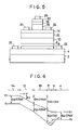
- FIGs. 5 and 6 The semiconductor device according to a first embodiment of the present invention will be explained in good detail using FIGs. 5 and 6.
- FIG. 5 shows a sectional view of the semiconductor device according to the first embodiment.
- n+-InGaAs sub-collector layer 4 with thickness of 500 nm is formed on an InP substrate 2.
- a quaternary alloy n+-(InGaAs) 0.4 (InAlAs) 0.6 wide-bandgap collector layer 8 with thickness of 50 nm is formed through a quaternary alloy n+-(InGaAs) 1-x (InAlAs) x graded layer 6 with thickness of 50 nm.
- InAlAs mole fraction x of the graded layer 6 varies from 0 to 0.6 continuously from the interface thereof with the sub-collector layer 4 to the interface thereof with the wide bandgap-collector layer 8.
- n-InAlAs emitter layer 16 with thickness of 200 nm is formed on the base layer 14.
- Collector electrodes 22, base electrodes 24, and an emitter electrode 26 are provided respectively on the sub-collector layer 4, the base layer 14 and the cap layer 20.
- an InAlAs/InGaAs HBT having a emitter provided by the InAlAs emitter layer 16, a base provided by the InGaAs base layer 14, and a collector provided by the InGaAs highly electron mobility collector layer 12, by the (InGaAs) 1-x (InAlAs) x breakdown-resistant collector layer 10 and by the (InGaAs) 0.4 (InAlAs) 0.6 wide bandgap collector layer 8.
- FIG. 6 shows the energy band structure of the base-collector of the semiconductor device of FIG. 5 in operation.
- the bandgaps Eg of the p+-InGaAs base layer 14 and the i-InGaAs high electron mobility collector layer 12 are 0.76 eV.
- the bandgap Eg of the i-(InGaAs) 1-x (InAlAs) x breakdown voltage collector layer 10 is a gradually changing bandgap which increases continuously from 0.76 eV at the interface thereof with the high electron mobility collector layer 12 to around 1.2 eV at the interface thereof with the wide bandgap collector layer 8 in accordance with the change of InAlAs mole fraction x.
- the bandgap Eg of the n+-(InGaAs) 0.4 (InAlAs) 0.6 wide bandgap collector layer 8 is around 1,2 eV but has a bending due to a high concentration of n+-doping.
- the bandgap Eg of the n+-(InGaAs) 1-x (InAlAs) x graded layer 6 is a gradually changing bandgap which decreases continuously from around 1.2 eV at the interface thereof with the wide bandgap collector layer 8 to 0.76 eV at the interface thereof with the sub-collector layer 4 in accordance with InAlAs mole fraction x.
- the bandgap Eg of the n+-InGaAs sub-collector 4 is 0.76 eV.
- the electrons flow at very high speed.
- the breakdown-resistant collector layer 10 its bandgap Eg increases continuously from 0.76 eV at the interface thereof with the high electron mobility collector layer 12 to around 1,2 eV at the interface thereof with the wide bandgap collector layer 8. Although kinetic energy of the electrons flowing in the breakdown-resistant layer 10 becomes gradually higher, the bandgap of the breakdown-resistant collector layer 10 is always lower than the kinetic enery of the electrons. Consequently the electrons flow in the breakdown-resistant collector layer 10 without causing the avalanche effect.
- the wide bandgap collector layer 8 its thickness is as thin as 50 nm but is heavily doped to be n+-type. Consequently an expansion of the depletion layer due to an base-collector applied voltage is accommodated in the wide bandgap collector layer 8, spaced a little from the interface of the breakdown-resistant collector layer 10. Accordingly decrease of the electron velocity due to the wide bandgap is not so effective to transit time.
- the base layer 14 and the high electron mobility collector layer 12 are made of InGaAs with narrow bandgaps, which is superior in electron mobility, electrons injected from the emitter layer 16 are allowed to flow at very high speed in the base layer 14 and the high electron mobility collector layer 12, and the bipolar transistor can be operative at high speed.
- the high electron mobility collector layer 12 not only has InGaAs with higher electron mobility, but also has an energy difference ⁇ E ⁇ -L between the ⁇ -valley and the L-valley relatively as high as 0.53 eV in comparison with InAlAs. This enables the electron velocity overshooting effect to be realized. Furthermore this is very effective to realize the speedup of the bipolar transistor.
- the gradually changing bandgap Eg is continuously widened in the direction of flow of electrons. Its bandgap is higher at respective positions thereof than kinetic energy Ek of the electrons flowing there, which allows the electrons flowing in the breakdown-resistant collector layer 10 to flow therethrough without the avalanche breakdown. Consequently high breakdown-voltage of the collector can be realized.
- the electrons flowing in the breakdown-resistant collector layer 10 do not flow "quasi-ballistically" and dispersed by the L-valley, etc., losing the kinetic energy Ek. Consequently the breakdown voltage can be made higher than the bandgap Eg widening in the direction of flow of electrons.
- the wide bandgap collector layer 8 is heavily doped to be n+-type, the expansion of the depletion layer can be confined within the wide bandgap collector layer 8. Consequently the breakdown voltage of the collector can be improved, and at the same time the decrease of mobility due to a wide bandgap little affects the electrons flowing through the wide bandgap collector layer 8.
- the high electron mobility collector layer 12 is preferablly more thick for reducing the transit time. But when the collector layer 12 is thick to excess, the kinetic energy Ek of electrons is too high to suppress the occurrence of the breakdown causes by the avalanche breakdown, with the breakdown voltage decreasing. Thus the thickness of the collector layer 12 is preferably the upper limit without causing the breakdown.
- the bandgap of the breakdown-resistant collector layer 10 changes gradually higher from the interface thereof with the high electron mobility collector layer 12. It is preferable for higher electron mobility and for reducing the transit time that the bandgap of the breakdown-resistant collector layer 10 changes more slightly. But when changes in the bandgap of the breakdown-resistant collector layer 10 are very slight, the kinetic energy Ek of electrons is too high to suppress the occurrence of the breakdown causes by the avalanche breakdown, with the breakdown voltage decreasing. Thus the bandgap of the breakdown-resistant collector layer 10 is preferably the lower limit without causing the breakdown.
- the limits of the kinetic energy Ek of electrons for the bandgap Eg without causing the avalanche breakdown to the breakdown will be explained below.
- Eg ⁇ Ek ⁇ 1.5Eg the limits of the kinetic energy Ek of electrons without causing the avalanche breakdown are given by Eg ⁇ Ek ⁇ 1.5Eg .
- the thickness of the high electron mobility collector layer 12 is determined so that the kinetic energy Ek of electrons flowing in the high electron mobility collector layer 12 is below 1.0 to 1.5 times the bandgap thereof.
- the changes in the bandgap of the breakdown-resistant collector layer 10 is determined so that the kinetic energy Ek of electrons flowing in the breakdown-resistant collector layer 10 is below 1.0 to 1.5 times the bandgap thereof.
- a preferable thickness range of the high electron mobility collector layer 12 will be explained in detail.
- Electrons injected from a base to a collector are accelerated by voltage applied between the base and the collector.
- the kinetic energy of electrons flowing in the collector differs depending on the voltage applied between the base and the collector.
- the preferable thickness range of the high electron mobility collector layer 12 differs depending on the voltage.
- An ECL gate of FIG. 7 will be selected as a typical circuit using HBTs according to the present invention.
- a transistor Tr1 has a collector connected to a collector supply voltage V CC through a resistor R1, and a base connected to an input voltage Vin.
- a transistor Tr2 has a collector connected to VCC through a resistor R2, and a base connected to an reference voltage Vr. Emitters of the transistors Tr1 and Tr2 are commonly connected to an emitter supply voltage V EE through a constant current source I1.
- a transistor Tr3 has a collector connected to V CC , a base connected to the collector of the transistor Tr2, and an emitter connected to V EE through a constant current source I2.
- An output voltage Vout is outputted from the emitter of the transistor Tr3.
- Vr V CC - Von - V1/2 where Von is a turn-on voltage of the HBT, and V1 a logic swing.
- Collector-base voltages Vbc which are applied between the collectors and the bases of the transistor Tr1, Tr2, and Tr3 are as follows respectively.
- the semiconductor device is an InAlAs/InGaAs heterojunction bipolar transistor, which have the emitter layer 16 made of n-InAlAs, and the base layer 14 made of p+-InGaAs.
- a turn-on voltage Von of the InAlAs/InGaAs HBT is about 0.80 volts.
- Vbc is a maximum of 0.60 volts.
- Vbc is a maximum of 1.20 volts.
- an electric field Fc ( Vbi + Vbc ) / Wc where Vbi is a build-in voltage between a base and a collector, Wc a width of the collector layer 12, and Eg a bandgap of the collector layer 12.
- d Wc x Eg x n / ( Vbi + Vbc ) .
- the thickness d of the high electron mobility collector layer 12 is given by When the HBT turns off, the thickness d of the high electron mobility collector layer 12 is given by
- the preferable thickness range of the high electron mobility collector layer 12 is 153.7 - 230.6 nm when the HBT turns on, or 109.4 - 164.2 nm when the HBT turns off.
- FIGs. 8 and 9 The semiconductor device according to a second embodiment of the present invention will be explained in good detail using FIGs. 8 and 9.
- FIG. 8 shows a sectional view of the semiconductor device according to the second embodiment.
- n+-InGaAs sub-collector layer 4 with thickness of 300 nm is formed on an InP substrate 2.
- an n-InP wide-bandgap collector layer 9 with thickness of 50 nm is formed through a quaternary alloy n+-InGaAsP graded layer 7 with thickness of 50 nm.
- a fraction of the graded layer 7 varies continuously from the interface thereof with the sub-collector layer 4 to the interface thereof with the wide bandgap-collector layer 9.
- a quaternary alloy i-InGaAsP breakdown-resistant collector layer 11 with thickness of 50 nm is formed on the wide-bandgap collector layer 9.
- n-InP emitter layer 17 with thickness of 200 nm is formed on the base layer 14.
- Collector electrodes 22, base electrodes 24, and an emitter electrode 26 are provided respectively on the sub-collector layer 4, the base layer 14 and the cap layer 20.
- an InP/InGaAs HBT having a emitter provided by the InP emitter layer 17, a base provided by the InGaAs base layer 14, and a collector provided by the InGaAs high electron mobility collector layer 12, by the InGaAsP breakdown-resistant collector layer 11 and by the InP wide bandgap collector layer 9.
- FIG. 9 shows the energy band structure of the base-collector of the semiconductor device of FIG. 8 in operation.
- the bandgaps Eg of the p+-InGaAs base layer 14 and the i-InGaAs high electron mobility collector layer 12 are 0.76 eV.
- the bandgap Eg of the i-InGaAsP breakdown voltage collector layer 11 is a gradually changing bandgap which increases continuously from 0.76 eV at the interface thereof with the high electron mobility collector layer 12 to around 1.35 eV at the interface thereof with the wide bandgap collector layer 9 in accordance with the change of mole fraction.
- the bandgap Eg of the n-InP wide bandgap collector layer 9 is around 1.35 eV.
- the bandgap Eg of the n+-InGaAsP graded layer 7 is a gradually changing bandgap which decreases continuously from around 1.35 eV at the interface thereof with the wide bandgap collector layer 9 to 0.76 eV at the interface thereof with the sub-collector layer 4 in accordance with mole fraction.
- the bandgap Eg of the n+-InGaAs sub-collector 4 is 0.76 eV.
- the breakdown-resistant collector layer 11 its bandgap Eg increases continuously from 0.76 eV at the interface thereof with the high electron mobility collector layer 12 to around 1.35 eV at the interface thereof with the wide bandgap collector layer 9. Although kinetic energy of the electrons flowing in the breakdown-resistant layer 11 becomes gradually higher, the bandgap of the breakdown-resistant collector layer 11 is always higher than the kinetic enery of the electrons. Consequently the electrons flow in the breakdown-resistant collector layer 11 without causing the avalanche breakdown.
- the base layer 14 and the high electron mobility collector layer 12 are made of InGaAs with narrow bandgaps, which is superior in electron mobility, electrons injected from the emitter layer 17 are allowed to flow at very high speed in the base layer 14 and the high electron mobility collector layer 12, and the bipolar transistor can be operative at high speed.
- the gradually changing bandgap Eg is continuously widened in the direction of flow of electrons. Its bandgap is higher at respective positions thereof than kinetic energy Ek of the electrons flowing there, which allows the electrons flowing in the breakdown-resistant collector layer 11 to flow therethrough without the avalanche breakdown. Consequently high breakdown-voltage of the collector can be realized.
- a preferable thickness range of the high electron mobility collector layer 12 of the InP/InGaAs HBT according to the second embodiment will be calculated by the same method as the HBT of the first embodiment.
- a turn-on voltage Von of the InP/InGaAs HBT is about 0.80 volts.
- Vbc is a maximum of 0.55 volts.
- the thickness d of the high electron mobility collector layer 12 is given by When the HBT turns on, the thickness d of the high electron mobility collector layer 12 is given by When the HBT turns off, the thickness d of the high electron mobility collector layer 12 is given by Thus the preferable thickness range of the high electron mobility collector layer 12 is 159.0 - 238.7 nm when the HBT turns on, or 112.1 - 168.2 nm when the HBT turns off.
- FIGs. 10 and 11 The semiconductor device according to a third embodiment of the present invention will be explained in good detail using FIGs. 10 and 11.
- FIG. 10 shows a sectional view of the semiconductor device according to the third embodiment.
- n+-GaAs sub-collector layer 34 with thickness of 500 nm is formed on a GaAs substrate 32.
- a n ⁇ -Al 0.75 Ga 0.25 As wide-bandgap collector layer 38 with thickness of 100 nm is formed through a n+-Al x Ga 1-x As graded layer 36 with thickness of 50 nm.
- AlAs mole fraction x of the graded layer 36 varies from 0.00 to 0.25 continuously from the interface thereof with the sub-collector layer 34 to the interface thereof with the wide bandgap-collector layer 38.
- An i-Al x Ga 1-x As breakdown-resistant collector layer 40 with thickness of 50 nm is formed on the wide-bandgap collector layer 38.
- AlAs mole fraction x of the breakdown-resistant collector layer 40 varies from 0.25 to 0.00 continuously from the interface thereof with the wide bandgap-collector layer 38 to the interface thereof with the high electron mobility collector layer 42.
- a p+-Al x Ga 1-x As base layer 44 with thickness of 100 nm is formed on the high electron mobility collector layer 42.
- On the base layer 44 is formed an n-Al x Ga 1-x As graded layer 45 with thickness of 50 nm.
- On the graded layer 45 is formed an n-Al 0.75 Ga 0.25 As emitter layer 46 with thickness of 150 nm.
- AlAs mole fraction x of the base layer 44 varies from 0.00 to 0.10 continuously from the interface thereof with the high electron mobility collector layer 42 to the interface thereof with the graded layer 45.
- AlAs mole fraction x of the graded layer 45 varies from 0.10 to 0.25 continuously from the interface thereof with the base layer 44 to the interface thereof with the emitter layer 46.
- AlAs mole fraction x of the graded layer 48 varies from 0.25 to 0.00 continuously from the interface thereof with the emitter layer 46 to the interface thereof with the cap layer 50.
- Collector electrodes 52, base electrodes 54, and an emitter electrode 56 are provided respectively on the sub-collector layer 34, the base layer 44 and the cap layer 50.
- an AlGaAs/GaAs HBT having a emitter made of AlGaAs, a base made of AlGaAs, and a collector made of GaAs and AlGaAs.
- FIG. 11 shows the energy band structure of the base-collector of the semiconductor device of FIG. 10 in operation.
- the bandgap Eg of the the p+-AlGaAs base layer 44 is a gradually changing bandgap which decreases continuously from 1.55 eV at the graded layer 45 to around 1.42 eV at the interface thereof with the interface thereof with the high electron mobility collector layer 42 in accordance with the change of AlAs mole fraction.
- the bandgaps Eg of the i-GaAs high electron mobility collector layer 42 are 1.42 eV.
- the bandgap Eg of the i-AlGaAs breakdown voltage collector layer 40 is a gradually changing bandgap which increases continuously from 1.42 eV at the interface thereof with the high electron mobility collector layer 42 to around 1.80 eV at the interface thereof with the wide bandgap collector layer 38 in accordance with the change of mole fraction.
- the bandgap Eg of the n-Al 0.75 Ga 0.25 As wide bandgap collector layer 38 is around 1.80 eV.
- the bandgap Eg of the n+Al x Ga 1-x As graded layer 36 is a gradually changing bandgap which decreases continuously from around 1.80 eV at the interface thereof with the wide bandgap collector layer 38 to 1.42 eV at the interface thereof with the sub-collector layer 34 in accordance with mole fraction.
- the bandgap Eg of the n+GaAs sub-collector 34 is 1.42 eV.
- the breakdown-resistant collector layer 40 its bandgap Eg increases continuously from 1.42 eV at the interface thereof with the high electron mobility collector layer 42 to around 1.80 eV at the interface thereof with the wide bandgap collector layer 38.
- kinetic energy of the electrons flowing in the breakdown-resistant collector layer 40 becomes gradually higher, the bandgap of the breakdown-resistant collector layer 40 is always higher than the kinetic enery of the electrons. Consequently the electrons flow in the breakdown-resistant collector layer 40 without causing the avalanche breakdown.
- the base layer 44 and the high electron mobility collector layer 42 are made of GaAs, electrons injected from the emitter layer 46 are allowed to flow at very high speed in the base layer 44 and the high electron mobility collector layer 42, and the bipolar transistor can be operative at high speed.
- the gradually changing bandgap Eg is continuously widened in the direction of flow of electrons. Its bandgap is higher at respective positions thereof than kinetic energy Ek of the electrons flowing there, which allows the electrons flowing in the breakdown-resistant collector layer 40 to flow therethrough without the avalanche breakdown. Consequently high breakdown-voltage of the collector can be realized.
- a preferable thickness range of the high electron mobility collector layer 42 of the AlGaAs/GaAs HBT according to the third embodiment will be calculated by the same method as the HBT of the first embodiment.
- a turn-on voltage Von of the AlGaAs/GaAs HBT is about 1.60 volts.
- Vbc is a maximum of 1.40 volts.
- the thickness d of the high electron mobility collector layer 42 is given by
- the preferable thickness range of the high electron mobility collector layer 42 is 145.6 - 218.4 nm when the HBT turns on, or 120.9 - 181.3 nm when the HBT turns off.
- both the breakdown-resistant collector layer 10, 11 or 40 and the high electron mobility collector layer 12 or 42 are formed to be i-type, but they may be p ⁇ -type or n ⁇ -type. Especially in the case of the p ⁇ -type, the band bending due to their doping further thickens the high electron mobility collector layer 12 or 42 enjoying high mobility. Consequently the speedup of the bipolar transistor can be further improved.
- the base layer 14 and the high electron mobility collector layer 12 are made of InGaAs but may be made of, e.g., Ge, SiGe or others.
- FIG. 12 shows a sectional view of the HBT according to the fourth embodiment.
- n+-InGaAs collector contact layer 64 with thickness of 300 to 500 nm is formed on an InP substrate 62.
- On the n+-InGaAs collector contact layer 64 are formed the following layers one on another in the sequence to be shown below; i.e., an n+-InGaAsP quaternary alloy graded layer 66 with thickness of 50 nm, an n+-InP wide bandgap collector layer 68 with thickness of 100 nm, a quaternary alloy n+-InGaAsP graded layer 70 with thickness of 50 nm, a p+-InGaAs planar doped layer 72 with thickness of 20 nm, an i-InGaAs narrow bandgap collector layer 74 with thickness of 200 nm, a p+-InGaAs base layer 76 with thickness of 50 to 100 nm, an n-InP emitter layer 78 with thickness of 200 nm, a quaternary
- Collector electrodes 84, base electrodes 86, and an emitter electrode 88 are formed respectively on the n+-InGaAs collector contact layer 64, the p+-InGaAs base layer 76, and the n+-InGaAs emitter contact layer 82.
- the quaternary alloy n+-InGaAsP graded layers 66, 70, 80 are (InP) x (InGaAs) 1-x where InP mole fraction x is varied from 1 to 0 or from 0 to 1.
- the p-type impurity concentrations of the p+-InGaAs base layer 76 and the p+-InGaAs planar doped layer 72 are so set that a concentration difference between the two concentrations can generate an electric field which maximizes the velocity-overshoot of transiting electrons in the i-InGaAs narrow bandgap collector layer 74.
- the n+-InGaAs collector contact layer 64 is for obtaining a low contact resistance.
- the quaternary alloy n+-InGaAsP graded layer 66 is for smoothly connecting the energy bands of the n+-InGaAs collector contact layer 64 and the n+-InP wide bandgap collector layer 68 so that no spike takes place in the conduction band of the junction therebetween.
- FIG. 13 is an energy bandgap structure of the HBT of FIG. 12.
- the emitter-base junction between the n-InP emitter layer 78 and the p+-InGaAs base layer 76 is an abrupt junction, and an around 0.3eV-spike is generated on the bottom of the conduct ion band Ec of the junction. Resultantly electrons injected from the n-InP emitter layer 78 to the p+-InGaAs base layer 76 have the hot electron effect and can transit at very high speed in the p+-InGaAs base layer 76.
- a turn-on voltage which is a voltage necessary to put this HBT turn on, is determined by the bandgap of the base layer.
- the effective electron mass of InGaAs which has a low bandgap, is small, and accordingly their characteristics of electron transport is quite good, which contributes to increasing transit speed of the electrons in the p+-InGaAs base layer 76 and their transit time in the base can be shortened.
- the electrons which have been transiting at very high speed in the p+-InGaAs base layer are injected into the i-InGaAs narrow bandgap collector layer 74.
- the i-InGaAs narrow bandgap collector layer 74 as well as the p+-InGaAs base layer 76 has a narrow bandgap and, at the same time, an i-type layer of a low impurity. Accordingly the scattering due to impurities is very little.
- the electric field in the i-InGaAs narrow bandgap collector layer 74 is so optimized that the velocity overshoot of the electrons is maximized due to a p-type impurity concentration difference between the p+-InGaAs base layer 76 and the p+-InGaAs planar doped layer 72. Consequently the electrons velocity overshoot in the entire region of the i-InGaAs narrow bandgap collector layer 74 and can transit quasi-ballistically in the ⁇ -valley where the transit speed is higher.
- Parts of the p+-InGaAs planar doped layer 72, the n+-InGaAsP quaternary alloy graded layer 70, and the n+-InP wide bandgap collector layer 68 are made depletion layers by the p+-n+ junction, with an intense electric field applied to.
- the electrons which have been transiting at ultra-high speed in the i-InGaAs narrow bandgap collector layer 74 enter this intense-field region.
- the avalanche breakdown of the electrons can be prevented because the bandgap of the quaternary alloy n+-InGaAsP graded layer 70 changes and widened gradually from 0.76 eV to 1.35 eV, and the bandgap of the n+-InP wide bandgap collector layer 68 is as wide as 1.35 eV. Consequently a sufficient collector breakdown voltage can be obtained.
- the electrons transit from the ⁇ -valley, where they have transited, to the L-valley.
- the distance over which the electrons transit in the L-valley is short because the width of the depletion layers do not widen because of high impurity concentrations of the n+-InGaAsP quaternary alloy graded layer 70 and the n+-InP wide bandgap collector layer 68. Consequently the depletion layers do not contribute much to the transit time.
- the turn-on voltage can be decreased to make a low power consumptive operation possible, the transit time in the base and the collector can be reduced to make an ultra-high speed operation possible, and a sufficiently high breakdown-voltage for the operation of circuits can be obtained because of the following features: 1) a spike generated on the bottom of the conduction band of the emitter-base junction between the n-InP emitter layer 78 and the p+-InGaAs layer 76 produces the hot electron effect; 2) both the p+-InGaAs base layer 76 and the i-InGaAs narrow bandgap collector layer 74 have narrow bandgaps; 3) the i-InGaAs narrow bandgap collector layer 74, the p+-InGaAs planar doped layer 72 and the n+-InGaAsP quaternary alloy layer 70 constitute an i/p+/n+ collector structure, and the electric field in the i-InGaAs narrow bandga
- the p+-type planar doped layer is provided by the p+-InGaAs planar doped layer 72 made of InGaAs, whose bandgap is narrow, as is the p+-InGaAs layer 76, but may be provided by a graded layer made of the same quaternary alloy InGaAsP as the quaternary alloy n-InGaAsP graded layer 70.
- an InGaAsP quaternary alloy graded layer whose bandgap is sloped and gradually widened is formed between the i-InGaAs narrow bandgap collector layer 74 and the n+-InP wide bandgap collector layer 68.
- the part of the InGaAsP quaternary alloy graded layer at the junction with the i-InGaAs narrow bandgap collector layer 74 is doped with a p-type impurity to form a quaternary alloy p+-InGaAsP planar doped layer 72, and the remainder of the InGaAsP quaternary alloy graded layer at the junction with the n+-InP wide bandgap collector layer 68 is doped with an n-type impurity to form an quaternary alloy n+-InGaAsP graded layer whose bandgap is continuous with that of the quaternary alloy p+-InGaAsP planar doped layer.
- This quaternary alloy p+-InGaAsP planer doped layer is depleted with an intense electric field applied to. For this reason, it is more preferable than the above-described embodiment, for the collector high breakdown voltage characteristic that the p+-InGaAsP quaternary alloy planer doped layer is a graded layer having a bandgap sloped and gradually widened.
- the collector layer contacting with the p+-InGaAs base layer 76 is provided by the i-InGaAs narrow bandgap collector layer 74, but it is not essential that the layer 74 is i-type and may be p-type or n-type. It is generally known that p-type is superior for the purpose of extending, at a low current density, the distance over which electrons transit in a ⁇ -valley for the speedup. But n-type is more preferable for the purpose of, at a high current density, preventing Kirk effect for the high speed operation.
- the n-InP emitter layer 78 is not limited to InP and may be, e.g., an n-InAlAs emitter layer.
- the InP layers may be InAlAs layers, and the InGaAsP layers may be InAlGaAs layers.
- the p+-InGaAs base layer 76 and the i-InGaAs narrow bandgap collector layer 74 are made of InGaAs, whose bandgap is narrow. But in the case the breakdown voltage is given preference to the speedup, it is not essential to use a semiconductor material with a narrow bandgap, and GaAs, for example, may be used.
Landscapes
- Bipolar Transistors (AREA)
Applications Claiming Priority (4)
| Application Number | Priority Date | Filing Date | Title |
|---|---|---|---|
| JP2102143A JP3046320B2 (ja) | 1990-04-18 | 1990-04-18 | 半導体装置 |
| JP102143/90 | 1990-04-18 | ||
| JP249088/90 | 1990-09-19 | ||
| JP2249088A JP3030070B2 (ja) | 1990-09-19 | 1990-09-19 | 半導体装置 |
Publications (2)
| Publication Number | Publication Date |
|---|---|
| EP0453945A1 true EP0453945A1 (de) | 1991-10-30 |
| EP0453945B1 EP0453945B1 (de) | 1997-10-08 |
Family
ID=26442879
Family Applications (1)
| Application Number | Title | Priority Date | Filing Date |
|---|---|---|---|
| EP91106160A Expired - Lifetime EP0453945B1 (de) | 1990-04-18 | 1991-04-17 | Bipolarer Transistor |
Country Status (3)
| Country | Link |
|---|---|
| US (1) | US5150185A (de) |
| EP (1) | EP0453945B1 (de) |
| DE (1) | DE69127849T2 (de) |
Families Citing this family (25)
| Publication number | Priority date | Publication date | Assignee | Title |
|---|---|---|---|---|
| EP0413333A3 (en) * | 1989-08-18 | 1991-07-24 | Hitachi, Ltd. | A superconductized semiconductor device |
| JP3130545B2 (ja) * | 1991-03-06 | 2001-01-31 | 株式会社東芝 | 半導体装置および半導体装置の製造方法 |
| US5270223A (en) * | 1991-06-28 | 1993-12-14 | Texas Instruments Incorporated | Multiple layer wide bandgap collector structure for bipolar transistors |
| US5508535A (en) * | 1992-01-09 | 1996-04-16 | Mitsubishi Denki Kabushiki Kaisha | Compound semiconductor devices |
| US5349201A (en) * | 1992-05-28 | 1994-09-20 | Hughes Aircraft Company | NPN heterojunction bipolar transistor including antimonide base formed on semi-insulating indium phosphide substrate |
| JPH0815214B2 (ja) * | 1993-03-12 | 1996-02-14 | 日本電気株式会社 | 量子細線構造 |
| JP3292894B2 (ja) * | 1993-05-12 | 2002-06-17 | 日本電信電話株式会社 | 集積化受光回路 |
| US5554882A (en) * | 1993-11-05 | 1996-09-10 | The Boeing Company | Integrated trigger injector for avalanche semiconductor switch devices |
| US5631477A (en) * | 1995-06-02 | 1997-05-20 | Trw Inc. | Quaternary collector InAlAs-InGaAlAs heterojunction bipolar transistor |
| US7692212B1 (en) * | 2004-12-07 | 2010-04-06 | Hrl Laboratories, Llc | Transistor with InGaAsP collector region and integrated opto-electronic devices employing same |
| US20020163013A1 (en) * | 2000-09-11 | 2002-11-07 | Kenji Toyoda | Heterojunction bipolar transistor |
| US6624449B1 (en) * | 2001-07-17 | 2003-09-23 | David C. Scott | Three terminal edge illuminated epilayer waveguide phototransistor |
| US7038224B2 (en) * | 2002-07-30 | 2006-05-02 | Applied Materials, Israel, Ltd. | Contact opening metrology |
| US7473911B2 (en) * | 2002-07-30 | 2009-01-06 | Applied Materials, Israel, Ltd. | Specimen current mapper |
| US6841795B2 (en) * | 2002-10-25 | 2005-01-11 | The University Of Connecticut | Semiconductor devices employing at least one modulation doped quantum well structure and one or more etch stop layers for accurate contact formation |
| JP4134715B2 (ja) * | 2002-12-19 | 2008-08-20 | 住友電気工業株式会社 | バイポーラトランジスタ |
| US7038250B2 (en) * | 2003-05-28 | 2006-05-02 | Kabushiki Kaisha Toshiba | Semiconductor device suited for a high frequency amplifier |
| US6841806B1 (en) * | 2003-06-24 | 2005-01-11 | The University Of Connecticut | Heterojunction thyristor-based amplifier |
| TWM253058U (en) * | 2003-09-05 | 2004-12-11 | Visual Photonics Epitaxy Co Lt | Heterogeneous junction dipole transistor structure for adjusting on voltage of base and emitter |
| KR100568567B1 (ko) * | 2003-12-19 | 2006-04-07 | 한국전자통신연구원 | 이종 접합 쌍극자 트랜지스터 및 그 제조 방법 |
| JP2007103784A (ja) * | 2005-10-06 | 2007-04-19 | Matsushita Electric Ind Co Ltd | ヘテロ接合バイポーラトランジスタ |
| CN102412285B (zh) * | 2011-11-01 | 2014-10-08 | 上海华虹宏力半导体制造有限公司 | 一种锗硅异质结三极管器件结构及其制造方法 |
| CN104995724B (zh) | 2013-02-18 | 2017-09-01 | 株式会社村田制作所 | 双极型晶体管 |
| CN105378904B (zh) * | 2013-07-10 | 2017-09-05 | 株式会社村田制作所 | 半导体装置 |
| US10263125B2 (en) * | 2014-05-16 | 2019-04-16 | Qorvo Us, Inc. | Varactor diode with heterostructure |
Citations (3)
| Publication number | Priority date | Publication date | Assignee | Title |
|---|---|---|---|---|
| EP0097767A2 (de) * | 1982-06-30 | 1984-01-11 | International Business Machines Corporation | Halbleitervorrichtung |
| EP0273363A2 (de) * | 1986-12-22 | 1988-07-06 | Nec Corporation | Bipolarer Heteroübergangs-Transistor mit ballistischem Betrieb |
| EP0278386A2 (de) * | 1987-02-06 | 1988-08-17 | Nippon Telegraph And Telephone Corporation | Bipolarer Transistor mit Heteroübergang |
-
1991
- 1991-04-12 US US07/684,385 patent/US5150185A/en not_active Expired - Lifetime
- 1991-04-17 DE DE69127849T patent/DE69127849T2/de not_active Expired - Fee Related
- 1991-04-17 EP EP91106160A patent/EP0453945B1/de not_active Expired - Lifetime
Patent Citations (3)
| Publication number | Priority date | Publication date | Assignee | Title |
|---|---|---|---|---|
| EP0097767A2 (de) * | 1982-06-30 | 1984-01-11 | International Business Machines Corporation | Halbleitervorrichtung |
| EP0273363A2 (de) * | 1986-12-22 | 1988-07-06 | Nec Corporation | Bipolarer Heteroübergangs-Transistor mit ballistischem Betrieb |
| EP0278386A2 (de) * | 1987-02-06 | 1988-08-17 | Nippon Telegraph And Telephone Corporation | Bipolarer Transistor mit Heteroübergang |
Non-Patent Citations (1)
| Title |
|---|
| APPLIED PHYSICS LETTERS vol. 53, no. 11, 12 September 1988, pages 983-985, New York, NY, US; W.T. TSANG et al.: "GaInAs/GaInAsP/InP heterostructure bipolar transistors with very thin base (150 A) grown by chemical beam epitaxy" * |
Also Published As
| Publication number | Publication date |
|---|---|
| US5150185A (en) | 1992-09-22 |
| DE69127849D1 (de) | 1997-11-13 |
| DE69127849T2 (de) | 1998-03-26 |
| EP0453945B1 (de) | 1997-10-08 |
Similar Documents
| Publication | Publication Date | Title |
|---|---|---|
| EP0453945B1 (de) | Bipolarer Transistor | |
| CA1237824A (en) | Resonant tunneling semiconductor device | |
| US6881988B2 (en) | Heterojunction bipolar transistor and semiconductor integrated circuit device using the same | |
| EP0313749B1 (de) | Bipolartransistor mit Heteroübergang | |
| EP1209750B1 (de) | NPN- Heteroübergang-Bipolartransistor mit einer Antimon enthaltenden Basis, der auf einem halb-isolierenden Indiumphosphid-Substrat hergestellt ist | |
| US4958208A (en) | Bipolar transistor with abrupt potential discontinuity in collector region | |
| JPH05243256A (ja) | ヘテロ接合バイポーラトランジスタおよびその製造方法 | |
| US5041882A (en) | Heterojunction bipolar transistor | |
| EP0603737A2 (de) | Hybrid-Bipolar/Feldeffekt-Leistungstransistor aus Material vom III-V-Typ | |
| US4716445A (en) | Heterojunction bipolar transistor having a base region of germanium | |
| EP0278386A2 (de) | Bipolarer Transistor mit Heteroübergang | |
| US4670767A (en) | Hetero-junction bipolar transistor having a high switching speed | |
| JPH0665216B2 (ja) | 半導体装置 | |
| EP0331482B1 (de) | Transistorstruktur | |
| EP0092645B1 (de) | Transistor und einen Transistor enthaltender Schaltkreis | |
| JP2505805B2 (ja) | ホットキャリアトランジスタ | |
| US5280182A (en) | Resonant tunneling transistor with barrier layers | |
| JP3046320B2 (ja) | 半導体装置 | |
| JP3030070B2 (ja) | 半導体装置 | |
| EP0186301A1 (de) | Halbleiteranordnung mit grosser Geschwindigkeit | |
| EP0322773B1 (de) | Halbleiterbauelement mit Halbmetall | |
| EP0229672B1 (de) | Bipolarer Heteroübergangstransistor mit einem Basisbereich aus Germanium | |
| EP0247667B1 (de) | Transistoren mit heissen Ladungsträgern | |
| US20250107128A1 (en) | Power Semiconductor Device and Method of Producing a Power Semiconductor Device | |
| GB2191035A (en) | Hot charge-carrier transistors |
Legal Events
| Date | Code | Title | Description |
|---|---|---|---|
| PUAI | Public reference made under article 153(3) epc to a published international application that has entered the european phase |
Free format text: ORIGINAL CODE: 0009012 |
|
| AK | Designated contracting states |
Kind code of ref document: A1 Designated state(s): DE FR GB |
|
| 17P | Request for examination filed |
Effective date: 19911017 |
|
| 17Q | First examination report despatched |
Effective date: 19941004 |
|
| GRAG | Despatch of communication of intention to grant |
Free format text: ORIGINAL CODE: EPIDOS AGRA |
|
| GRAH | Despatch of communication of intention to grant a patent |
Free format text: ORIGINAL CODE: EPIDOS IGRA |
|
| GRAH | Despatch of communication of intention to grant a patent |
Free format text: ORIGINAL CODE: EPIDOS IGRA |
|
| GRAA | (expected) grant |
Free format text: ORIGINAL CODE: 0009210 |
|
| AK | Designated contracting states |
Kind code of ref document: B1 Designated state(s): DE FR GB |
|
| REF | Corresponds to: |
Ref document number: 69127849 Country of ref document: DE Date of ref document: 19971113 |
|
| ET | Fr: translation filed | ||
| PLBE | No opposition filed within time limit |
Free format text: ORIGINAL CODE: 0009261 |
|
| STAA | Information on the status of an ep patent application or granted ep patent |
Free format text: STATUS: NO OPPOSITION FILED WITHIN TIME LIMIT |
|
| 26N | No opposition filed | ||
| REG | Reference to a national code |
Ref country code: GB Ref legal event code: IF02 |
|
| PGFP | Annual fee paid to national office [announced via postgrant information from national office to epo] |
Ref country code: FR Payment date: 20060410 Year of fee payment: 16 |
|
| PGFP | Annual fee paid to national office [announced via postgrant information from national office to epo] |
Ref country code: GB Payment date: 20060412 Year of fee payment: 16 |
|
| PGFP | Annual fee paid to national office [announced via postgrant information from national office to epo] |
Ref country code: DE Payment date: 20060413 Year of fee payment: 16 |
|
| GBPC | Gb: european patent ceased through non-payment of renewal fee |
Effective date: 20070417 |
|
| PG25 | Lapsed in a contracting state [announced via postgrant information from national office to epo] |
Ref country code: DE Free format text: LAPSE BECAUSE OF NON-PAYMENT OF DUE FEES Effective date: 20071101 |
|
| PG25 | Lapsed in a contracting state [announced via postgrant information from national office to epo] |
Ref country code: GB Free format text: LAPSE BECAUSE OF NON-PAYMENT OF DUE FEES Effective date: 20070417 |
|
| PG25 | Lapsed in a contracting state [announced via postgrant information from national office to epo] |
Ref country code: FR Free format text: LAPSE BECAUSE OF NON-PAYMENT OF DUE FEES Effective date: 20070430 |