EP0454001B1 - Vertikalablenkungssystem im geschalteten Betrieb - Google Patents
Vertikalablenkungssystem im geschalteten Betrieb Download PDFInfo
- Publication number
- EP0454001B1 EP0454001B1 EP91106381A EP91106381A EP0454001B1 EP 0454001 B1 EP0454001 B1 EP 0454001B1 EP 91106381 A EP91106381 A EP 91106381A EP 91106381 A EP91106381 A EP 91106381A EP 0454001 B1 EP0454001 B1 EP 0454001B1
- Authority
- EP
- European Patent Office
- Prior art keywords
- signal
- vertical
- coupled
- amplifier
- deflection
- Prior art date
- Legal status (The legal status is an assumption and is not a legal conclusion. Google has not performed a legal analysis and makes no representation as to the accuracy of the status listed.)
- Expired - Lifetime
Links
- 239000003990 capacitor Substances 0.000 claims description 28
- 230000008859 change Effects 0.000 description 16
- 238000004804 winding Methods 0.000 description 10
- 230000001052 transient effect Effects 0.000 description 5
- XUIMIQQOPSSXEZ-UHFFFAOYSA-N Silicon Chemical compound [Si] XUIMIQQOPSSXEZ-UHFFFAOYSA-N 0.000 description 4
- 230000008878 coupling Effects 0.000 description 4
- 238000010168 coupling process Methods 0.000 description 4
- 238000005859 coupling reaction Methods 0.000 description 4
- 238000010586 diagram Methods 0.000 description 4
- 229910052710 silicon Inorganic materials 0.000 description 4
- 239000010703 silicon Substances 0.000 description 4
- 230000002411 adverse Effects 0.000 description 3
- 230000001934 delay Effects 0.000 description 2
- 238000007599 discharging Methods 0.000 description 2
- 230000000694 effects Effects 0.000 description 2
- 230000000750 progressive effect Effects 0.000 description 2
- 230000004044 response Effects 0.000 description 2
- 230000002441 reversible effect Effects 0.000 description 2
- 230000009471 action Effects 0.000 description 1
- 238000013016 damping Methods 0.000 description 1
- 230000003247 decreasing effect Effects 0.000 description 1
- 230000000977 initiatory effect Effects 0.000 description 1
- 230000010354 integration Effects 0.000 description 1
- 230000007704 transition Effects 0.000 description 1
Images

Classifications
-
- H—ELECTRICITY
- H04—ELECTRIC COMMUNICATION TECHNIQUE
- H04N—PICTORIAL COMMUNICATION, e.g. TELEVISION
- H04N3/00—Scanning details of television systems; Combination thereof with generation of supply voltages
- H04N3/10—Scanning details of television systems; Combination thereof with generation of supply voltages by means not exclusively optical-mechanical
- H04N3/16—Scanning details of television systems; Combination thereof with generation of supply voltages by means not exclusively optical-mechanical by deflecting electron beam in cathode-ray tube, e.g. scanning corrections
-
- H—ELECTRICITY
- H03—ELECTRONIC CIRCUITRY
- H03K—PULSE TECHNIQUE
- H03K4/00—Generating pulses having essentially a finite slope or stepped portions
- H03K4/06—Generating pulses having essentially a finite slope or stepped portions having triangular shape
- H03K4/08—Generating pulses having essentially a finite slope or stepped portions having triangular shape having sawtooth shape
- H03K4/83—Generating pulses having essentially a finite slope or stepped portions having triangular shape having sawtooth shape using as active elements semiconductor devices with more than two PN junctions or with more than three electrodes or more than one electrode connected to the same conductivity region
- H03K4/835—Generating pulses having essentially a finite slope or stepped portions having triangular shape having sawtooth shape using as active elements semiconductor devices with more than two PN junctions or with more than three electrodes or more than one electrode connected to the same conductivity region using pulse-modulation techniques for the generation of the sawtooth wave, e.g. class D, switched mode
Definitions
- This invention relates generally to the field of deflection systems for televisions, and in particular, to switched mode vertical deflection systems and control circuits for same.
- Switched mode vertical deflection systems derive power from horizontal deflection energy, by storing a portion of a horizontal trace or retrace energy each horizontal deflection cycle.
- the energy is supplied to a vertical deflection winding in order to provide the desired vertical deflection current in the deflection winding.
- the amount of horizontal rate energy stored each horizontal interval is closely controlled in order to provide the correct amount of vertical deflection current.
- a typical output stage for a switched mode vertical deflection system may include a thyristor, for example a silicon controlled rectifier, coupled in parallel with a diode.
- the cathode of the thyristor and the anode of the diode are coupled to ground.
- the ungrounded terminals of the thyristor and diode are coupled in series with a storage coil and a winding of the integrated high voltage transformer (IHVT) and the vertical yoke, or deflection coil.
- IHVT integrated high voltage transformer
- a storage capacitor may be coupled between the junction of the winding of the integrated high voltage transformer and the vertical yoke and ground. Horizontal retrace pulses are coupled through the integrated high voltage transformer to the winding.
- the thyristor and diode, and the storage coil effect horizontal rate charging and discharging of the storage capacitor, the storage capacitor supplying vertical deflection current.
- switched mode deflection circuits including the one described above, are illustrated in U.S. patent 4,544,864-Haferl.
- Such a switched mode vertical deflection system can be controlled by pulses supplied to the gate of the silicon controlled rectifier, to control conduction thereof.
- control circuits often comprise a comparator, for example an operational amplifier, having a horizontal rate ramp signal as one input and a vertical rate ramp signal as another input.
- the vertical rate ramp signal may be generated by a conventional ramp generating circuit which supplies DC current to an integrator, for example a capacitor, which is periodically reset at a vertical rate, for example by vertical reset pulses.
- the vertical rate ramp signal is combined with a feedback signal related to vertical deflection current.
- the feedback signal may have a DC component, an AC component, or both.
- the horizontal rate ramp generator for the horizontal rate ramp signal may also be powered by horizontal flyback pulses.
- the horizontal rate ramp signal is developed from clipped flyback pulses which are AC coupled to an integrator.
- the resulting ramp is added to an independently generated DC reference level and coupled to one input of the amplifier or comparator, for example the inverting input.
- the independently generated DC reference level sets the DC reference level for the output of the amplifier or comparator.
- a horizontal rate ramp generator as described above can cause distortion of the raster.
- the AC coupling of the flyback pulses has an inherent time constant, which can adversely affect the vertical rate feedback gain and can adversely affect linearity.
- such an arrangement was thought to be necessary in order to avoid distortion of the horizontal rate ramp signal due to amplitude variations of the horizontal flyback pulses.
- Amplitude variations of horizontal flyback pulses can result from variations in beam current loading and from transient disturbances during the transition from vertical retrace to vertical trace.
- Vertical rate timing disturbances particularly in switched mode vertical systems, can alter the amplitude, period and width of the horizontal flyback pulses. The timing disturbance is of course at a vertical rate.
- the AC coupling of such an arrangement also makes it necessary to generate the DC reference level for the amplifier or comparator.
- a deflection system according to the preamble of claim 1 is disclosed in US-A-3 939 380.
- a circuit for recovering energy from unutilized power is shown which contains means for establishing a substantially constant DC voltage reference level.
- the horizontal flyback pulses are utilized for generating a horizontal rate ramp with only DC coupling through to the amplifier or comparator, rather than AC coupling.
- the DC reference level of the horizontal rate ramp signal sets the DC reference level for the amplifier or comparator.
- a switched mode deflection system comprises: a switched mode deflection output stage for driving a deflection coil; a negative feedback path for a feedback signal related to deflection current; and, a generator for a first deflection rate waveform.
- a control circuit comprises a signal generator and a comparator.
- the signal generator is coupled to a source of flyback pulses for developing from energy in the flyback pulses a second deflection rate waveform having a predetermined and substantially constant DC voltage reference level set by operation of the signal generator.
- the comparator has a first input coupled for receiving the second deflection rate waveform, has a second input coupled for receiving the first deflection rate waveform and the feedback signal and has an output controlling switching in the output stage.
- the amplifier output has a DC voltage reference level corresponding to the DC reference level of the first deflection rate waveform.
- the signal generator is DC coupled between the source of flyback pulses and the comparator.
- a switched mode vertical deflection system comprises: a switched mode vertical deflection output stage for driving a vertical deflection coil; a feedback circuit for generating a feedback signal related to vertical deflection current; and, a circuit for generating a vertical rate ramp signal
- the comparator or amplifier has an output controlling switching in the output stage.
- the first input of the comparator for example a noninverting input, is coupled for receiving the vertical rate ramp signal and the feedback signal.
- the signal generator is DC coupled between the source of horizontal flyback pulses and the second input of the comparator, for example an inverting input, for developing from energy in the horizontal flyback pulses a horizontal rate ramp signal having a predetermined and substantially constant DC voltage reference level.
- the amplifier output has a DC voltage reference level corresponding to the DC reference level of the horizontal rate ramp signal.
- a deflection system comprises: a signal generator, an amplifier, a negative feedback path and a vertical rate waveform generator.
- the signal generator is coupled to a source of flyback pulses for developing from energy in the flyback pulses a horizontal rate drive signal having a predetermined and substantially constant DC voltage reference level.
- the amplifier has a first input coupled for receiving the horizontal rate drive signal and an output coupled to a deflection coil.
- the amplifier output has a DC voltage reference level corresponding to the DC reference level of the horizontal rate drive signal.
- a DC feedback signal on the negative feedback path is related to deflection current.
- the feedback path is coupled between the coil and a second input of the amplifier.
- the vertical rate waveform is also coupled to the second input of the amplifier for modulating the horizontal rate drive signal.
- the output of the amplifier is a pulse width modulated control signal for a switching element, for example a silicon controlled rectifier.
- the timing control circuit for vertical deflection can assume a free running mode during channel change, when vertical synchronizing pulses are no longer available.
- the free running frequency is somewhat slower than the normal vertical deflection rate. This increases the period and amplitude of the vertical rate ramp signal, which can disturb the vertical position of on screen displays during channel change.
- An adjustment of the vertical rate ramp, in either period or slope, or both must be made in order to avoid disturbing such on screen displays.
- a control signal can be generated, for example by a microprocessor, for initiating such a change in the vertical rate ramp generator.
- a transistor switch may be activated to change the time constant of the ramp generating network, for example, during channel change.
- the switch responsive to a channel change related control signal can be held positively and intentionally in a conductive condition for an additional predetermined period of time, in order for the transient disturbances associated with reestablishing vertical sync to dissipate.
- a capacitor is charged by the control signal, which also provides base drive for a transistor switch. The capacitor remains charged, and can not begin discharging, until after the control signal terminates. After termination of the control signal, current from the capacitor can maintain base drive of the transistor switch for a predetermined period time, for example, approximately three milliseconds.
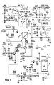
- FIGURE 1 is a circuit schematic for a switched mode vertical deflection system having a control circuit in accordance with aspects of this invention.
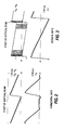
- FIGURES 2 and 3 are waveform diagrams useful for illustrating operation of the deflection system shown in FIGURE 1 near the start of vertical scanning.
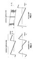
- FIGURES 4 and 5 are waveform diagrams useful for illustrating operation of the deflection system shown in FIGURE 1 near the center of vertical scanning.
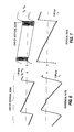
- FIGURES 6 and 7 are waveform diagrams useful for illustrating operation of the deflection system shown in FIGURE 1 near the end of vertical scanning.
- FIGURES 8 and 9 are waveform diagrams useful for illustrating operation of the deflection system shown in FIGURE 1 at vertical retrace.
- a switched mode vertical deflection system and control circuit comprises generally an output stage 10, a feedback stage 12, a vertical rate ramp stage 14, a horizontal rate ramp stage 16 and a vertical rate ramp modifying stage 18, operable during channel change.
- diode D4 is conductive during the horizontal retrace interval. Current flows from ground through the diode D4, through storage coil L and winding W of the integrated high voltage transformer, to charge capacitor C11. The charge on capacitor C11 causes a deflection current to flow from capacitor C11 through the coil of the vertical deflection yoke.
- a thyristor for example silicon controlled rectifier SCR is conductive during a portion of a horizontal trace interval.
- Resistor R23 is connected in parallel with the deflection yoke as a yoke damping resistor. Resistor R20 provides vertical centering.
- Feedback stage 12 receives a vertical rate, generally parabolic feedback signal V 1 .
- the yoke current I Y is AC coupled by capacitor C3 to sense resistor R5.
- An AC feedback signal component V 2 related to deflection current is coupled through resistor R10 to a summing junction 20.
- a DC feedback signal path through resistors R11 and R12 is also coupled to summing junction 20.
- the DC feedback signal path includes an RC network comprising capacitor C20 and resistor R13. This network effects an integration of the generally parabolic feedback signal to provide a generally S-shaped feedback signal V 3 , also related to deflection current.
- Vertical rate ramp stage 14 includes a transistor Q6 coupled in emitter-follower configuration. Flyback pulses coupled to a resistor network including resistors R14, R22 and R39 are rectified by diode D2 to develop a DC voltage source across capacitor C4 and resistor R43. During normal operation, other than during channel change, the DC bias on the base of transistor Q6 is fixed by resistors R7 and R4. The DC signal is integrated by capacitor C19, to develop a ramp. Vertical reset pulses V 5 coupled through resistor R1 to the base of transistor Q5 periodically cause conduction of transistor Q5 to discharge capacitor C19 at the vertical deflection rate. The pulse width of the vertical reset pulses is designated T VR . Pulse width T VR is reflected in waveforms V 4 and V 6 .
- the base of transistor Q5 is biased by resistor R3.
- the result is a vertical rate ramp V 4 at the base of Q6, which appears with only slightly reduced amplitude at the emitter of transistor Q6.
- a feedback path formed by resistor R21 and capacitor C18 distort the ramp to be slightly parabolic as shown by signal V 10 , in order to compensate for certain distortion in the feedback paths.
- the vertical rate ramp signal is coupled to summing junction 20 through resistor R9.
- Resistor R22 is a variable resistor which provides for variable height adjustment.
- Control circuit 16 includes a comparator U1 and a horizontal rate ramp generator formed by Zener diode Z1, capacitor C22 and resistor R26, which are coupled in parallel with one another.
- the terminal of the parallel combination including the anode of Zener diode Z1 is grounded.
- the terminal of the parallel combination connected to the cathode of Zener diode Z1 is coupled to one input of comparator U1, for example an inverting input, and to the cathode of diode D1.
- the horizontal rate waveform is generated from energy in the flyback pulses because the horizontal rate ramp generator, having no active switches or amplifiers, is a passive network. Flyback pulses are coupled to the anode of diode D1 through resistor R42.
- comparator U1 Another input of comparator U1, for example a noninverting input, is coupled to summing junction 20. Waveform V 6 reflects the combination of vertical rate ramp V 4 , AC feedback signal V 2 and DC feedback signal V 3 .
- the output of comparator U1 is coupled to the gate of the SCR through resistor R19.
- the control circuit 16 develops both the DC voltage reference level and the horizontal rate reference ramp required for controlling the switched mode vertical output stage.
- Comparator U1 functions as a combination error amplifier and voltage to phase converter.
- current through resistor R42 initially charges capacitor C22 to the rated voltage Zener diode Z1, 6.2 volts for the example shown. Thereafter, current supplied through resistor R42 flows to ground through the Zener diode. After the flyback pulse ends, diode D1 becomes reverse biased. Capacitor C22 then discharges through resistor R26 defining the required ramp. The resulting ramp is substantially independent of variations in the amplitude of the flyback pulses of voltage signal V 7 .
- the reference Zener can be driven to the full I ZT specification with negligible power, due to the small duty cycle of the Zener current.
- the DC reference level of the ramp signal becomes the DC reference level for the output of the comparator.
- the DC reference level need not be set independently of the ramp signal.
- Each successive ramp shape pulse of signal V 8 will be sampled at a different and successively higher level by vertical rate ramp V 6 . This provides the necessary modulation in gating conduction of the SCR to provide vertical deflection current.
- the upper waveform reflects the output of the comparator U1, namely the difference of signal V 8 - signal V 6 .
- the lower waveform is the current I L through the storage coil and transformer winding, and the time scale is the horizontal deflection rate.
- the lower waveform is the current I Y through the yoke, and the time scale is the vertical deflection rate.
- the time position of the waveforms in FIGURE 2, shown in the expanded time scale of the horizontal rate, is indicated by the dark vertical bar and corresponding legend Start of Vertical Scan in FIGURE 3.
- the time position of the waveforms in FIGURE 4, shown in the expanded time scale of the horizontal rate, is indicated by the dark vertical bar and corresponding legend Center of Vertical Scan in FIGURE 5.
- the time position of the waveforms in FIGURE 6, shown in the expanded time scale of the horizontal rate, is indicated by the dark vertical bar and corresponding legend End of Vertical Scan in FIGURE 7.
- the time position of the waveforms in FIGURE 8, shown in the expanded time scale of the horizontal rate, is indicated by the dark vertical bar and corresponding legend Vertical Retrace in FIGURE 9.
- Horizontal retrace pulses forward bias the diode D4.
- Current I L flows from ground through diode D4, through coil L and through winding W to charge capacitor C11.
- Diode D4 becomes reverse biased during horizontal trace and stops conducting.
- Capacitor C11 discharges during horizontal trace, causing deflection or yoke current I Y to flow through the vertical deflection coil.
- Current I L and therefore current I Y , would be substantially constant, but for the action of the SCR.
- the SCR conducts responsive to gating pulses supplied by the comparator U1. The gating pulses occur during a portion of each horizontal trace interval.
- FIGURES 2 and 3 near the start of vertical scanning, the SCR is gated on for a near minimum time, current I L is mostly positive and deflection current I Y is near maximum.
- FIGURES 4 and 5 near the center of vertical scanning, the SCR is gated on for near to half way between minimum and maximum, current I L is approximately half positive and half negative, and deflection current I Y is near to half way between minimum and maximum.
- FIGURES 6 and 7 near the end of vertical scanning, the SCR is gated is gated on for a near to maximum time, The current I L is much more negative than positive, and the deflection current I Y is near to minimum.
- the SCR is turned off because no gating pulses are provided by the comparator during most of the duration of the vertical reset pulse, shown in waveform V 5 .
- the diode D4 is forward biased during part of each horizontal retrace pulse, providing positive current I L to charge capacitor C11.
- Capacitor C11 is also charged by energy stored in the inductance of the vertical deflection coil.
- the horizontal rate ramp generator is DC coupled between the source of horizontal flyback pulses and the noninverting input of the comparator U1. This improves the transient response of the entire control system, as the control system is not prone to adverse disturbance of vertical feedback gain and disturbance of raster linearity. Moreover, the horizontal rate ramp signal can be generated with a predetermined DC reference level, with many fewer components than generally required.
- Changing channels can result in the loss of synchronizing signals.
- Many timing control circuits for vertical deflection systems assume a free running mode of operation at a frequency slightly lower than the vertical deflection frequency when vertical synchronizing pulses are lost. This prevents vertical collapse of the raster, and subsequent damage to the cathode ray tube.
- the time between successive vertical reset pulses in signal V 5 will be increased during the free running mode, as a consequence of the reduced frequency.
- the increased time between adjacent vertical reset pulses results in the amplitude of the vertical rate ramp V 4 increasing undesirably, which can in turn disturb the position of on screen displays which are intended to remain in place during channel change.
- Vertical rate ramp modifying circuit 18 compensates for this undesirable amplitude variation of the vertical rate ramp signal V 4 .
- a microprocessor 30 controlling many functions of a television generates, inter alia , a channel change (CH. CHG.) signal V 9 coupled to the base of transistor switch Q4 through resistor R49.
- Resistor R44 is coupled from the channel change output pin to a +5 volt supply, which is also coupled to the collector of transistor Q4.
- a network comprising resistors R46 and R50 and capacitor C27 provides an output signal designated SYNC KILL used elsewhere in the television system.
- the channel change signal is also coupled to the output pin of the microprocessor designated TV PIX by diode D3. Accordingly, the output of the channel change pin can generate a TV PIX signal, but a TV PIX output will not be effective as a channel change control signal.
- the junction of resistor R50 and diode D3 is an on screen display position control signal designated OSD POS.
- Diode D11 becomes forward biased when transistors Q4 conducts, charging capacitor C25 and providing base drive to transistor Q7 through resistor R16.
- the base of transistor Q7 is biased by resistor R46.
- resistor R45 is coupled in series between the junction of resistor R4 and the collector of Q5, and ground. This effectively changes the DC reference of the vertical rate ramp signal V 4 , so that the maximum amplitude corresponds more closely to the maximum amplitude when vertical sync is present. Accordingly, many on screen displays can remain substantially in position during channel change, particularly those positioned near the top of the raster, such as channel numbers. In the absence of a channel change control signal, the operation of vertical rate ramp circuit 14 is not affected.
Landscapes
- Engineering & Computer Science (AREA)
- Multimedia (AREA)
- Signal Processing (AREA)
- Details Of Television Scanning (AREA)
Claims (7)
- Ablenksystem, umfassend:ein passives Netzwerk (16), das mit einer Quelle von Rücklaufimpulsen (V7) zur Erzeugung eines horizontalfrequenten Ansteuersignals (V8) aus Energie in den Rücklaufimpulsen (V7) verbunden ist;einen Verstärker (U1, 10) zum Empfang des horizontalfrequenten Ansteuersignals (V8) an einem ersten Eingang und zur Erzeugung eines impulsbreitenmodulierten Steuersignals zur Ansteuerung einer Ablenkspule;eine Rückkopplungssignal-Stufe (12) für ein auf den Ablenkstrom bezogenes Signal (V1), das von der Spule einem zweiten Eingang des Verstärkers (U1, 10) zugeführt wird; undMittel (14) zur Erzeugung einer vertikalfrequenten Wellenform, die dem zweiten Eingang des Verstärkers (U1, 10) zugeführt wird; dadurch gekennzeichnet,daß das passive Netzwerk (16) Mittel (Z1) zur Errichtung eines vorgegebenen und im wesentlichen konstanten Gleichspannungs-Bezugspegels für das Ansteuersignal (V8) aufweist, der im wesentlichen unabhängig von Amplitudenänderungen der Rücklaufimpulse (V7) ist, und daß die Rückkopplungssignal-Stufe (12) parallele Signalwege für negative Wechselstrom-(V2)- und Gleichstrom -(V3)-Rückkopplungssignale hat.
- System nach Anspruch 1, bei dem das passive Netzwerk (16) durch eine ZENER-Diode (Z1), einen Kondensator (C22) und einen Widerstand (R26) in einem parallelen Netzwerk gekennzeichnet ist, wobei ein Verbindungspunkt des Netzwerks (16) mit einem der Verstärker-Eingänge und der andere Verbindungspunkt mit Masse verbunden ist.
- System nach Anspruch 1 oder 2, bei dem der Verstärker (U1, 10) gekennzeichnet ist durch:eine Vergleichsstufe (U1), die das impulsbreitenmodulierte Steuersignal erzeugt, das auf das horizontalfrequente Ansteuersignal (V8), die vertikalfrequente Wellenform (V4) und das Rückkopplungssignal (V1) anspricht; undeine geschaltete Ausgangsstufe (10), die durch das impulsbreitenmodulierte Signal gesteuert wird.
- System nach Anspruch 1, 2 oder 3, dadurch gekennzeichnet, daß das horizontalfrequente Ansteuersignal und die vertikalfrequente Wellenform Rampensignale sind.
- System nach einem der vorhergehenden Ansprüche, dadurch gekennzeichnet, daß das passive Netzwerk (16) eine ZENER-Diode (Z1) umfaßt, um einen maximalen Amplitudenpegel für das horizontalfreuente Ansteuersignal (V8) und einen Gleichstrom-Bezugspegel für den Verstärker-Ausgang festzulegen.
- System nach einem der vorhergehenden Ansprüche, dadurch gekennzeichnet, daß das passive Netzwerk (16) zwischen der Quelle der Rücklaufimpulse (V7) und dem Verstärker (U1, 10) gleichstrommäßig gekoppelt ist.
- System nach einem der vorhergehenden Ansprüche, dadurch gekennzeichnet, daß die Rückkopplungsstufe (12) ein integrierendes Netzwerk enthält.
Applications Claiming Priority (2)
| Application Number | Priority Date | Filing Date | Title |
|---|---|---|---|
| US515901 | 1990-04-27 | ||
| US07/515,901 US4999549A (en) | 1990-04-27 | 1990-04-27 | Switched mode vertical deflection system and control circuit |
Publications (3)
| Publication Number | Publication Date |
|---|---|
| EP0454001A2 EP0454001A2 (de) | 1991-10-30 |
| EP0454001A3 EP0454001A3 (en) | 1992-03-25 |
| EP0454001B1 true EP0454001B1 (de) | 1997-07-16 |
Family
ID=24053242
Family Applications (1)
| Application Number | Title | Priority Date | Filing Date |
|---|---|---|---|
| EP91106381A Expired - Lifetime EP0454001B1 (de) | 1990-04-27 | 1991-04-20 | Vertikalablenkungssystem im geschalteten Betrieb |
Country Status (11)
| Country | Link |
|---|---|
| US (1) | US4999549A (de) |
| EP (1) | EP0454001B1 (de) |
| JP (1) | JP3464493B2 (de) |
| KR (1) | KR100229970B1 (de) |
| CN (1) | CN1034786C (de) |
| CA (1) | CA2039781C (de) |
| DE (1) | DE69126819T2 (de) |
| FI (1) | FI102996B (de) |
| MY (1) | MY105410A (de) |
| SG (1) | SG85054A1 (de) |
| TR (1) | TR24970A (de) |
Families Citing this family (5)
| Publication number | Priority date | Publication date | Assignee | Title |
|---|---|---|---|---|
| GB9004392D0 (en) * | 1990-02-27 | 1990-04-25 | Rca Licensing Corp | Raster corrected vertical deflection circuit |
| US5198731A (en) * | 1992-06-15 | 1993-03-30 | Thomson Consumer Electronics S.A. | Linearization of vertical reference ramp |
| FR2753326B1 (fr) * | 1996-09-09 | 1998-11-27 | Sgs Thomson Microelectronics | Dispositif de detection de verrouillage d'un circuit de controle automatique de gain |
| US6515439B2 (en) * | 2000-12-25 | 2003-02-04 | Sanyo Electric Co., Ltd. | Vertical deflection driving circuit |
| US20070096826A1 (en) * | 2005-10-27 | 2007-05-03 | Kolb Lowell E | Methods and system of feedback in amplifier circuit |
Citations (1)
| Publication number | Priority date | Publication date | Assignee | Title |
|---|---|---|---|---|
| US4814672A (en) * | 1987-03-12 | 1989-03-21 | Deutsche Thomson-Brandt Gmbh | Circuitry for limiting an operating voltage obtained by way of a rectifier from a secondary winding of a transformer |
Family Cites Families (8)
| Publication number | Priority date | Publication date | Assignee | Title |
|---|---|---|---|---|
| US3939380A (en) * | 1974-02-21 | 1976-02-17 | Rca Corporation | Class D amplifier |
| GB1528981A (en) * | 1975-02-20 | 1978-10-18 | Rca Corp | Deflection system such as for television receivers including a switched mode vertical(field)reflection circuit |
| GB1560600A (en) * | 1976-02-04 | 1980-02-06 | Rca Corp | Conduction overlap control circuit |
| US4234826A (en) * | 1979-06-28 | 1980-11-18 | Rca Corporation | Synchronous switched vertical deflection driven during both trace and retrace intervals |
| FR2497045A1 (fr) * | 1980-12-23 | 1982-06-25 | Thomson Brandt | Circuit de balayage vertical, alimentation pour sa commande et recepteur de television comportant un tel circuit |
| GB8304755D0 (en) * | 1983-02-21 | 1983-03-23 | Rca Corp | Switched vertical deflection circuit |
| IT1228252B (it) * | 1987-07-02 | 1991-06-05 | Sgs Microelettronica Spa Catan | Circuito di deflessione verticale per gioghi di cinescopi, con generatore di tensione di rintraccia |
| US4795949A (en) * | 1988-04-08 | 1989-01-03 | Rca Licensing Corporation | Deflection current correction circuit |
-
1990
- 1990-04-27 US US07/515,901 patent/US4999549A/en not_active Expired - Lifetime
-
1991
- 1991-04-04 CA CA002039781A patent/CA2039781C/en not_active Expired - Fee Related
- 1991-04-08 MY MYPI91000576A patent/MY105410A/en unknown
- 1991-04-20 DE DE69126819T patent/DE69126819T2/de not_active Expired - Fee Related
- 1991-04-20 EP EP91106381A patent/EP0454001B1/de not_active Expired - Lifetime
- 1991-04-20 SG SG9602298A patent/SG85054A1/en unknown
- 1991-04-23 JP JP12208091A patent/JP3464493B2/ja not_active Expired - Fee Related
- 1991-04-23 KR KR1019910006474A patent/KR100229970B1/ko not_active Expired - Fee Related
- 1991-04-25 TR TR91/0387A patent/TR24970A/xx unknown
- 1991-04-26 CN CN91102733A patent/CN1034786C/zh not_active Expired - Fee Related
- 1991-04-26 FI FI912028A patent/FI102996B/fi not_active IP Right Cessation
Patent Citations (1)
| Publication number | Priority date | Publication date | Assignee | Title |
|---|---|---|---|---|
| US4814672A (en) * | 1987-03-12 | 1989-03-21 | Deutsche Thomson-Brandt Gmbh | Circuitry for limiting an operating voltage obtained by way of a rectifier from a secondary winding of a transformer |
Also Published As
| Publication number | Publication date |
|---|---|
| FI102996B1 (fi) | 1999-03-31 |
| JPH0795432A (ja) | 1995-04-07 |
| MY105410A (en) | 1994-09-30 |
| TR24970A (tr) | 1992-09-01 |
| CA2039781C (en) | 1997-01-21 |
| US4999549A (en) | 1991-03-12 |
| CA2039781A1 (en) | 1991-10-28 |
| CN1056198A (zh) | 1991-11-13 |
| EP0454001A3 (en) | 1992-03-25 |
| FI912028A0 (fi) | 1991-04-26 |
| FI912028A7 (fi) | 1991-10-28 |
| FI102996B (fi) | 1999-03-31 |
| DE69126819T2 (de) | 1998-01-08 |
| CN1034786C (zh) | 1997-04-30 |
| DE69126819D1 (de) | 1997-08-21 |
| SG85054A1 (en) | 2001-12-19 |
| EP0454001A2 (de) | 1991-10-30 |
| KR910019388A (ko) | 1991-11-30 |
| JP3464493B2 (ja) | 2003-11-10 |
| KR100229970B1 (ko) | 1999-11-15 |
Similar Documents
| Publication | Publication Date | Title |
|---|---|---|
| US4048544A (en) | Switched vertical deflection system | |
| JPH0227870B2 (de) | ||
| EP0367101B1 (de) | Fernsehgerät mit Schaltnetzteil | |
| EP0211569B1 (de) | Ablenkungsschaltung mit Modulatorschaltung mit Schaltmodus | |
| HK1000196B (en) | A deflection circuit with a switched mode modulator circuit | |
| US4999549A (en) | Switched mode vertical deflection system and control circuit | |
| US4385264A (en) | Start-up circuit for a power supply | |
| US6124686A (en) | Horizontal deflection circuit | |
| CA1069611A (en) | Vertical deflection circuit | |
| KR0137274B1 (ko) | 비디오 표시장치의 수직 편향회로 | |
| EP0528176A1 (de) | Linearitätskontrollvorrichtung für Horizontalablenkstufe | |
| US5089755A (en) | Vertical deflection circuit | |
| EP0332091B1 (de) | Ablenkungsschaltung mit Rasterverzerrungskorrektur | |
| JP3458961B2 (ja) | 偏向回路 | |
| HK1004318B (en) | Raster distortion corrected deflection circuit | |
| US5796217A (en) | Picture display apparatus with a soft-start device | |
| EP0504687B1 (de) | Ablenkschaltung mit einer Rückkopplungsanordnung | |
| WO1999057888A1 (en) | Horizontal deflection circuit | |
| JPH11127364A (ja) | 水平偏向回路 | |
| KR20010022025A (ko) | 수평편향회로 | |
| JP3230717B2 (ja) | 水平偏向高圧発生回路 | |
| KR820000207B1 (ko) | 시간 교정 수평 편향 회로 | |
| KR800000397B1 (ko) | 수직 편향 회로 | |
| JPH0546377Y2 (de) | ||
| HK1004317A1 (en) | Protection arrangement of a deflection circuit |
Legal Events
| Date | Code | Title | Description |
|---|---|---|---|
| PUAI | Public reference made under article 153(3) epc to a published international application that has entered the european phase |
Free format text: ORIGINAL CODE: 0009012 |
|
| AK | Designated contracting states |
Kind code of ref document: A2 Designated state(s): DE FR GB IT |
|
| PUAL | Search report despatched |
Free format text: ORIGINAL CODE: 0009013 |
|
| AK | Designated contracting states |
Kind code of ref document: A3 Designated state(s): DE FR GB IT |
|
| 17P | Request for examination filed |
Effective date: 19920820 |
|
| 17Q | First examination report despatched |
Effective date: 19950315 |
|
| GRAG | Despatch of communication of intention to grant |
Free format text: ORIGINAL CODE: EPIDOS AGRA |
|
| GRAH | Despatch of communication of intention to grant a patent |
Free format text: ORIGINAL CODE: EPIDOS IGRA |
|
| GRAH | Despatch of communication of intention to grant a patent |
Free format text: ORIGINAL CODE: EPIDOS IGRA |
|
| GRAA | (expected) grant |
Free format text: ORIGINAL CODE: 0009210 |
|
| AK | Designated contracting states |
Kind code of ref document: B1 Designated state(s): DE FR GB IT |
|
| REF | Corresponds to: |
Ref document number: 69126819 Country of ref document: DE Date of ref document: 19970821 |
|
| ET | Fr: translation filed | ||
| ITF | It: translation for a ep patent filed | ||
| PLBE | No opposition filed within time limit |
Free format text: ORIGINAL CODE: 0009261 |
|
| STAA | Information on the status of an ep patent application or granted ep patent |
Free format text: STATUS: NO OPPOSITION FILED WITHIN TIME LIMIT |
|
| 26N | No opposition filed | ||
| REG | Reference to a national code |
Ref country code: GB Ref legal event code: IF02 |
|
| REG | Reference to a national code |
Ref country code: FR Ref legal event code: D6 |
|
| REG | Reference to a national code |
Ref country code: GB Ref legal event code: 746 Effective date: 20030103 |
|
| PGFP | Annual fee paid to national office [announced via postgrant information from national office to epo] |
Ref country code: GB Payment date: 20060303 Year of fee payment: 16 |
|
| PGFP | Annual fee paid to national office [announced via postgrant information from national office to epo] |
Ref country code: FR Payment date: 20060421 Year of fee payment: 16 |
|
| PGFP | Annual fee paid to national office [announced via postgrant information from national office to epo] |
Ref country code: IT Payment date: 20060430 Year of fee payment: 16 |
|
| GBPC | Gb: european patent ceased through non-payment of renewal fee |
Effective date: 20070420 |
|
| PG25 | Lapsed in a contracting state [announced via postgrant information from national office to epo] |
Ref country code: GB Free format text: LAPSE BECAUSE OF NON-PAYMENT OF DUE FEES Effective date: 20070420 |
|
| PG25 | Lapsed in a contracting state [announced via postgrant information from national office to epo] |
Ref country code: FR Free format text: LAPSE BECAUSE OF NON-PAYMENT OF DUE FEES Effective date: 20070430 |
|
| PGFP | Annual fee paid to national office [announced via postgrant information from national office to epo] |
Ref country code: DE Payment date: 20080422 Year of fee payment: 18 |
|
| PG25 | Lapsed in a contracting state [announced via postgrant information from national office to epo] |
Ref country code: IT Free format text: LAPSE BECAUSE OF NON-PAYMENT OF DUE FEES Effective date: 20070420 |
|
| PG25 | Lapsed in a contracting state [announced via postgrant information from national office to epo] |
Ref country code: DE Free format text: LAPSE BECAUSE OF NON-PAYMENT OF DUE FEES Effective date: 20091103 |