EP0454050A2 - Integrated circuit device for processing signals - Google Patents
Integrated circuit device for processing signals Download PDFInfo
- Publication number
- EP0454050A2 EP0454050A2 EP91106507A EP91106507A EP0454050A2 EP 0454050 A2 EP0454050 A2 EP 0454050A2 EP 91106507 A EP91106507 A EP 91106507A EP 91106507 A EP91106507 A EP 91106507A EP 0454050 A2 EP0454050 A2 EP 0454050A2
- Authority
- EP
- European Patent Office
- Prior art keywords
- data
- instruction
- memory
- program
- storing
- Prior art date
- Legal status (The legal status is an assumption and is not a legal conclusion. Google has not performed a legal analysis and makes no representation as to the accuracy of the status listed.)
- Granted
Links
Images



Classifications
-
- H—ELECTRICITY
- H03—ELECTRONIC CIRCUITRY
- H03H—IMPEDANCE NETWORKS, e.g. RESONANT CIRCUITS; RESONATORS
- H03H17/00—Networks using digital techniques
- H03H17/02—Frequency selective networks
- H03H17/06—Non-recursive filters
-
- G—PHYSICS
- G06—COMPUTING OR CALCULATING; COUNTING
- G06F—ELECTRIC DIGITAL DATA PROCESSING
- G06F17/00—Digital computing or data processing equipment or methods, specially adapted for specific functions
-
- G—PHYSICS
- G06—COMPUTING OR CALCULATING; COUNTING
- G06F—ELECTRIC DIGITAL DATA PROCESSING
- G06F7/00—Methods or arrangements for processing data by operating upon the order or content of the data handled
- G06F7/38—Methods or arrangements for performing computations using exclusively denominational number representation, e.g. using binary, ternary, decimal representation
- G06F7/48—Methods or arrangements for performing computations using exclusively denominational number representation, e.g. using binary, ternary, decimal representation using non-contact-making devices, e.g. tube, solid state device; using unspecified devices
- G06F7/544—Methods or arrangements for performing computations using exclusively denominational number representation, e.g. using binary, ternary, decimal representation using non-contact-making devices, e.g. tube, solid state device; using unspecified devices for evaluating functions by calculation
- G06F7/5443—Sum of products
Definitions
- This invention relates to an integrated circuit device for processing signals, which is suitable for performing multiply-accumulation, such as a non-recursive digital filter, hereinafter called "FIR (Finite Impulse Response) filter".
- FIR Finite Impulse Response
- DSP digital signal processor
- ALU Arimetic and Logic Unit
- DSPs are controlled by programs each consisting of a series of instruction code items. They are designed for general purposes, and hence are able not only to serve as FIR filter, but also to perform ordinary operations.
- a DSP serving as FIR filter will be explained.
- Fig. 1 shows a conventional DSP.
- a program-address generator 3 generates an address, whereby either a program memory 1a built within the DSP or a program memory 1b provided outside is accessed, and instruction data is read out.
- An instruction decoder 5 converts the read-out data to control signals 13a - 13h to be supplied to various processing units.
- the data to be used for operations are stored in data memories 2a and 2b, and have respective addresses to be accessed by data memory-address generators 4a and 4b.
- a multiplier 8 and an ALU 9 are independent from each other, and are connected to each other, by buses 7 and 12a - 12m, which are dedicated to data transmission between the memories 2a and 2b and registers 10a and 10b for storing calculated results.
- the control signals 13a - 13h output from the instruction decoder 5 are supplied to data bus selectors 11a - 11e for switching the buses, also to the ALU 9 for designating an operation, and to the registers 10a and 10b for latching control.
- the buses 7 and 12a - 12m are separated from a program data bus 6, two memories 2a and 2b are employed, and the multiplier 8 and ALU 9 are connected in tandem for performing a great number of product-cumulations.
- many DSPs incorporate ROMs for storing, as coefficient data, program data and a part of data to be stored in the data memories.
- the calculation performed by the FIR filter is given by where y represents the output of the filter, xi an input variable, and ai a coefficient.
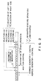
- Fig. 2 shows a instruction code to be used in the calculation.
- the operation of each processing unit is controlled by "0" or "1" designated in a corresponding bit position a - h.
- the data in the a-bit position instructs whether or not "1” should be added to an address to be generated from the address generator 4a, while the data in the b-bit position instructs whether or not "1" should be added to an address to be generated from the address generator 4b.
- Each data in bit-positions c, d, f, g, and h controls a corresponding one of the selectors 11a - 11e to select data input from one side thereof when it is "1", and controls it to select data input from the other side when it is "0".
- the data in the e-bit (8 - 1) positions instruct operations.
- the data in an 8-bit position thereof designates an addition
- the data in 1 - 7 positions designate operations other than the addition.
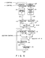
- n-coefficients ai and n-input data xi are stored in the memories 2a and 2b, respectively, as is shown in Fig. 5.
- the multiplier 8 carries out the multiplication ai ⁇ xi.
- the operation result is supplied to the ALU 9 and added to the result Si-1 which was obtained in the last occasion.
- the selectors 11a - 11e select processing units, respectively, and control the ALU 9 to perform the addition.
- the instruction code controls each of the address generators 4a and 4b to increase its address by one, so that the n-coefficients ai and n-input variables xi will be accessed subsequently.
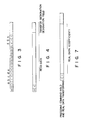
- the immediate data items to be loaded in memories exist in the instruction code as shown in Fig. 4, and occupy a greater part of the word length of the code.
- the DSP must be installed in the system, since the DSP has to be executed in real time.
- the coefficient ai need be adjusted, with the DSP installed in the associated system.
- the DSP must operate at a speed identical to that at which it actually operates, and further the program and the coefficient ai must be easily changed.
- the coefficient ai is not stored together with the program, so that it cannot be changed in a way similar to ordinary programs, resulting in a low efficiency.
- the program is stored in a ROM 1b arranged outside the integrated circuit device, or a RAM or EPROM arranged in the device.
- RAMs stores data less than ROMs.
- EPROMs are not suitable for high-speed operation, since much access time is required.
- a ROM arranged outside is generally used for storing the program.
- terminals for an address bus and a data bus are required.
- ROMs in which data cannot be rewritten are not suitable for storing the coefficient ai in an adaptive-type filter, since the coefficient ai is not a constant in the filter.
- double RAMs it is more advantageous to employ double RAMs than to employ a ROM dedicated to storing the coefficient ai.
- the RAM stores constant data at all times, resulting in a low efficiency of the DSP.
- This invention has been made to overcome the above disadvantages, and aims to provide an integrated circuit device for processing signals which can operate at high speed, also alter the coefficient data with ease, and thus operate effectively.
- the integrated circuit device of the invention comprises: calculation means including a data-storing memory to be controlled by a instruction code, a multiplier, an ALU, a register for storing a calculated result, data buses for connecting the above components to one another, and selectors for switching the data buses, and instruction control means including a program address generator for accessing a program memory provided in or outside the device for storing the instruction code, a data bus terminal for receiving the instruction code read from the outside program memory, a instruction decoder for decoding the read-out instruction code and transmitting control signals to the calculation means to control it, and a instruction transfer bus for connecting the program memory to the instruction decoder; characterized in that coefficient data is stored in the program memory, together with the instruction code, and a register is provided for storing the instruction code read from the program memory so that the coefficient data will be accessed on a continuous basis, and calculation is performed continuously.
- the coefficient data since the coefficient data is stored in the program memory, together with the instruction code, the coefficient data can be altered in a way similar to ordinary programs, and no memories dedicated to storing the coefficient data are required, thereby reducing the number of required terminals.
- the invention incorporates a register for storing the instruction code read from the program memory, so that the coefficient data can be accessed continuously without interrupting the operation of the program, and product cumulation and the like can be repeated continuously, thereby reducing the time required for processing.
- the data-storing memory need not store the coefficient data at all times, so that the entire area of the memory can be used for storing those variable data other than the coefficient data which are required for calculation.
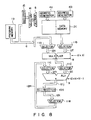
- Figs. 6A and 6B show the device of the invention.
- This device is similar to the conventional one shown in Fig. 4 except that it has a register 15 and a selector 16 both arranged between the program memory 1a and decoder 5.
- the same elements as those shown in Fig. 4 are designated by the same reference numerals, and explanations thereof are omitted.
- the register 15 stores a instruction code read out of the memory 1a, while the selector 16 switches program data buses to select either data read out of the register 15 or data read out of the memory 1a.
- the selector 16 is controlled by most significant bit data in the program data bus.
- the register 15 stores the instruction code which was used in the calculation performed in the a instruction execution cycle immediately before the present cycle.
- the instruction code shown in Fig. 7 is used which differs from the conventional one in that it has "1" designated in its most signification fit. By virtue of this, when this instruction code is read out of the memory 1a, the register 15 is selected for the decoder 5.
- Fig. 8 is a flowchart of data.
- the register 15 stores a instruction which was effected in a instruction execution cycle immediately before the present cycle, and the program memory 1a continuously stores a instruction for transferring the immediate data to the program data bus 6.
- the immediate data is transferred as the coefficient ai to the multiplier 8 on a continuous basis.
- the processing speed can be kept at high level.
- the memory 1a serves not only as memory for storing the instruction code but also as memory for storing the coefficient ai
- the coefficient ai can be altered in a way similar to ordinary programs, when the program employed is debugged in a state where the DSP is installed.
- the altering can be done with high efficiency, and neither a dedicated signal terminal nor a memory dedicated to storing the coefficient ai is required.
- the coefficients ai need not be stored at all times in the data memory 2c, the entire area thereof can be used for storing the variables xi, thereby enabling the device to be used effectively.
- the present invention is not limited to the above-described embodiment.
- a dual-port memory (RAM) is used as the data memory 2c, it may be replaced with such a conventional RAM as consists of independent double memory cell arrays.
- the structure of the DSP is not limited to that shown in Figs. 6A and 6B.
- the DSP suffices if it incorporates an operational unit and a memory which can perform, by the use of a coefficient data group, such arithmetic operations as the FIR filter performs, also if a constant coefficient data group is stored in a program memory together with a instruction code, and if a register for storing an instruction code is employed so that calculation will be performed on a continuous basis and the constant coefficient data items are accessed on a continuous basis.
- the instruction code is not limited to those shown in Figs. 2 - 4, and 7.
- the FIR filter performs product cumulation.
- the invention is applicable not also to this filter, but also to other cases where calculation is repeated by the use of a coefficient data group and a variable data group.
- command code-storing register 15 is employed, if more than two registers are used alternately, not only a simple-formula calculation but also a complex-polynomial calculation can be repeated.
- the coefficient data group is stored in the program memory together with a instruction code, so that a memory dedicated to storing coefficient data is not required.
- a register which stores a command code read out of the program memory, and hence the coefficient data can be accessed on a continuous basis without interrupting the flow of the program, thereby enabling calculation such as product cumulation to be repeated.
- the device of the invention can operate at high speed.
- coefficient data group is stored in the program memory together with the instruction code, it can be altered in a way similar to ordinary programs.
- the entire area of the memory can be used for storing those variable data other than the coefficient data which are required for calculation, which enables the device to be used effectively.
Landscapes
- Engineering & Computer Science (AREA)
- Physics & Mathematics (AREA)
- Theoretical Computer Science (AREA)
- General Physics & Mathematics (AREA)
- Mathematical Physics (AREA)
- General Engineering & Computer Science (AREA)
- Computing Systems (AREA)
- Databases & Information Systems (AREA)
- Data Mining & Analysis (AREA)
- Computer Hardware Design (AREA)
- Computational Mathematics (AREA)
- Software Systems (AREA)
- Mathematical Analysis (AREA)
- Mathematical Optimization (AREA)
- Pure & Applied Mathematics (AREA)
- Complex Calculations (AREA)
- Executing Machine-Instructions (AREA)
- Memory System (AREA)
Abstract
Description
- This invention relates to an integrated circuit device for processing signals, which is suitable for performing multiply-accumulation, such as a non-recursive digital filter, hereinafter called "FIR (Finite Impulse Response) filter".
- In general, digital signals are processed by repeating algebraic operations, particularly by performing product-cumulation. Since the amount of the operations are excessively large, the digital signal processor (hereinafter called "DSP") dedicated to signal processing employs operation-accelerating devices such as a high-speed multiplier and ALU (Arithmetic and Logic Unit).
- Like general microprocessors, DSPs are controlled by programs each consisting of a series of instruction code items. They are designed for general purposes, and hence are able not only to serve as FIR filter, but also to perform ordinary operations. Here, a DSP serving as FIR filter will be explained.
- Fig. 1 shows a conventional DSP. As is shown in the figure, a program-
address generator 3 generates an address, whereby either a program memory 1a built within the DSP or aprogram memory 1b provided outside is accessed, and instruction data is read out. Aninstruction decoder 5 converts the read-out data to controlsignals 13a - 13h to be supplied to various processing units. The data to be used for operations are stored indata memories 2a and 2b, and have respective addresses to be accessed by data memory-address generators - For performing product-cumulation, a
multiplier 8 and anALU 9 are independent from each other, and are connected to each other, by buses 7 and 12a - 12m, which are dedicated to data transmission between thememories 2a and 2b and registers 10a and 10b for storing calculated results. The control signals 13a - 13h output from theinstruction decoder 5 are supplied todata bus selectors 11a - 11e for switching the buses, also to theALU 9 for designating an operation, and to the registers 10a and 10b for latching control. - To increase the processing speed, the buses 7 and 12a - 12m are separated from a
program data bus 6, twomemories 2a and 2b are employed, and themultiplier 8 and ALU 9 are connected in tandem for performing a great number of product-cumulations. Further, to increase the accessing speed, many DSPs incorporate ROMs for storing, as coefficient data, program data and a part of data to be stored in the data memories. - The calculation performed by the FIR filter is given by

where y represents the output of the filter, xi an input variable, and ai a coefficient. - Fig. 2 shows a instruction code to be used in the calculation. The operation of each processing unit is controlled by "0" or "1" designated in a corresponding bit position a - h. The data in the a-bit position instructs whether or not "1" should be added to an address to be generated from the
address generator 4a, while the data in the b-bit position instructs whether or not "1" should be added to an address to be generated from theaddress generator 4b. Each data in bit-positions c, d, f, g, and h controls a corresponding one of theselectors 11a - 11e to select data input from one side thereof when it is "1", and controls it to select data input from the other side when it is "0". The data in the e-bit (8 - 1) positions instruct operations. The data in an 8-bit position thereof designates an addition, and the data in 1 - 7 positions designate operations other than the addition. - To perform the calculation (1) by means of the above instruction code, n-coefficients ai and n-input data xi are stored in the
memories 2a and 2b, respectively, as is shown in Fig. 5. Then, themultiplier 8 carries out the multiplication ai·xi. The operation result is supplied to theALU 9 and added to the result Si-1 which was obtained in the last occasion. Subsequently, theselectors 11a - 11e select processing units, respectively, and control theALU 9 to perform the addition. Thus, the calculation of the polynomial (1) is performed for one item i (i = 1 to n). Each time the calculation for one item has been performed, the instruction code controls each of theaddress generators - The above-described FIR filter has the following disadvantages:
- The immediate data items to be loaded in memories exist in the instruction code as shown in Fig. 4, and occupy a greater part of the word length of the code. The larger the number of the immediate data items, the smaller the number of the other data items for instruction the calculation, so that the calculation may be interrupted, resulting in a reduction in calculation efficiency.
- Further, for debugging or alteration of the program for the DSP, the DSP must be installed in the system, since the DSP has to be executed in real time.
- To determine whether or not the frequency characteristics of the DSP accord to desired ones, or to change them, by using the FIR filter, the coefficient ai need be adjusted, with the DSP installed in the associated system. To this end, the DSP must operate at a speed identical to that at which it actually operates, and further the program and the coefficient ai must be easily changed. In the conventional DSP, however, the coefficient ai is not stored together with the program, so that it cannot be changed in a way similar to ordinary programs, resulting in a low efficiency.
- Moreover, as is shown in Fig.1, the program is stored in a
ROM 1b arranged outside the integrated circuit device, or a RAM or EPROM arranged in the device. RAMs stores data less than ROMs. EPROMs are not suitable for high-speed operation, since much access time is required. Thus, a ROM arranged outside is generally used for storing the program. In the case of providing the ROM in the device, terminals for an address bus and a data bus are required. - The same can be said of a memory for the coefficient ai. In the case of providing a ROM in the device, terminals for an address bus and a data bus are required.
- To avoid this, it can be thought that the program data and coefficient ai are stored in the same ROM. In this case, however, the program data must be accessed at a time different from that at which the coefficient ai is accessed. This is disadvantageous to the DSP which has to operate at high speed.
- ROMs in which data cannot be rewritten are not suitable for storing the coefficient ai in an adaptive-type filter, since the coefficient ai is not a constant in the filter. Thus, to design the DSP for general purposes, it is more advantageous to employ double RAMs than to employ a ROM dedicated to storing the coefficient ai. In the case of using a RAM, however, if the coefficient ai is a constant, the RAM stores constant data at all times, resulting in a low efficiency of the DSP.
- This invention has been made to overcome the above disadvantages, and aims to provide an integrated circuit device for processing signals which can operate at high speed, also alter the coefficient data with ease, and thus operate effectively.
- To this end, the integrated circuit device of the invention comprises:
calculation means including a data-storing memory to be controlled by a instruction code, a multiplier, an ALU, a register for storing a calculated result, data buses for connecting the above components to one another, and selectors for switching the data buses, and
instruction control means including a program address generator for accessing a program memory provided in or outside the device for storing the instruction code, a data bus terminal for receiving the instruction code read from the outside program memory, a instruction decoder for decoding the read-out instruction code and transmitting control signals to the calculation means to control it, and a instruction transfer bus for connecting the program memory to the instruction decoder;
characterized in that coefficient data is stored in the program memory, together with the instruction code, and a register is provided for storing the instruction code read from the program memory so that the coefficient data will be accessed on a continuous basis, and calculation is performed continuously. - In the integrated circuit device of the invention, since the coefficient data is stored in the program memory, together with the instruction code, the coefficient data can be altered in a way similar to ordinary programs, and no memories dedicated to storing the coefficient data are required, thereby reducing the number of required terminals.
- Further, the invention incorporates a register for storing the instruction code read from the program memory, so that the coefficient data can be accessed continuously without interrupting the operation of the program, and product cumulation and the like can be repeated continuously, thereby reducing the time required for processing. In addition, the data-storing memory need not store the coefficient data at all times, so that the entire area of the memory can be used for storing those variable data other than the coefficient data which are required for calculation.
- This invention can be more fully understood from the following detailed description when taken in conjunction with the accompanying drawings, in which:
- Fig. 1 is a circuit diagram showing a conventional signal-processing integrated circuit;
- Figs. 2 - 4 are views showing a instruction code to be used in the circuit shown in Fig. 1;
- Fig. 5 is a block diagram, useful in explaining the operation of a DSP incorporated in the circuit shown in Fig. 1 and serving as FIR filter;
- Figs. 6A and 6B are circuit diagrams showing a signal-processing integrated circuit device according to an embodiment of the present invention;
- Fig. 7 is a view showing a instruction code to be used in the circuit shown in Figs. 6A and 6B; and
- Fig. 8 is a block diagram, useful in explaining the operation of a DSP incorporated in the circuit shown in Figs. 6A and 6B and serving as FIR filter.
- The invention will be explained with reference to the accompanying drawings showing an embodiment thereof.
- Figs. 6A and 6B show the device of the invention. This device is similar to the conventional one shown in Fig. 4 except that it has a
register 15 and aselector 16 both arranged between the program memory 1a anddecoder 5. The same elements as those shown in Fig. 4 are designated by the same reference numerals, and explanations thereof are omitted. Theregister 15 stores a instruction code read out of the memory 1a, while theselector 16 switches program data buses to select either data read out of theregister 15 or data read out of the memory 1a. Theselector 16 is controlled by most significant bit data in the program data bus. - The
register 15 stores the instruction code which was used in the calculation performed in the a instruction execution cycle immediately before the present cycle. In the present invention, the instruction code shown in Fig. 7 is used which differs from the conventional one in that it has "1" designated in its most signification fit. By virtue of this, when this instruction code is read out of the memory 1a, theregister 15 is selected for thedecoder 5. - The calculation performed by the DSP serving as FIR filter will now be explained. Fig. 8 is a flowchart of data.
- After the instruction code shown in Fig. 3 for making the DSP serve as FIR filter is altered such that data flows as shown in Fig. 8, the altered instruction is effected. The
register 15 stores a instruction which was effected in a instruction execution cycle immediately before the present cycle, and the program memory 1a continuously stores a instruction for transferring the immediate data to theprogram data bus 6. With this structure, the immediate data is transferred as the coefficient ai to themultiplier 8 on a continuous basis. - Since the program memory 1a stores both the instruction code and the coefficient ai, and the instruction is effected without interruption while the coefficient ai is being accessed, the processing speed can be kept at high level.
- Further, since the memory 1a serves not only as memory for storing the instruction code but also as memory for storing the coefficient ai, the coefficient ai can be altered in a way similar to ordinary programs, when the program employed is debugged in a state where the DSP is installed. Thus, the altering can be done with high efficiency, and neither a dedicated signal terminal nor a memory dedicated to storing the coefficient ai is required.
- Since unlike the conventional device, the coefficients ai need not be stored at all times in the data memory 2c, the entire area thereof can be used for storing the variables xi, thereby enabling the device to be used effectively.
- The present invention is not limited to the above-described embodiment. For example, although in the embodiment, a dual-port memory (RAM) is used as the data memory 2c, it may be replaced with such a conventional RAM as consists of independent double memory cell arrays. Further, the structure of the DSP is not limited to that shown in Figs. 6A and 6B. The DSP suffices if it incorporates an operational unit and a memory which can perform, by the use of a coefficient data group, such arithmetic operations as the FIR filter performs, also if a constant coefficient data group is stored in a program memory together with a instruction code, and if a register for storing an instruction code is employed so that calculation will be performed on a continuous basis and the constant coefficient data items are accessed on a continuous basis. The instruction code is not limited to those shown in Figs. 2 - 4, and 7.
- In the embodiment, the FIR filter performs product cumulation. The invention, however, is applicable not also to this filter, but also to other cases where calculation is repeated by the use of a coefficient data group and a variable data group.
- In addition, although in the embodiment, the command code-storing
register 15 is employed, if more than two registers are used alternately, not only a simple-formula calculation but also a complex-polynomial calculation can be repeated. - If it is apprehended that the instruction code which should be stored in the
register 15 will be decoded, and that undesired processing will be effected, such a trouble can be avoided only by providing a field for prohibiting decoding. - As is described above, in the invention, the coefficient data group is stored in the program memory together with a instruction code, so that a memory dedicated to storing coefficient data is not required.
- Further, a register is employed which stores a command code read out of the program memory, and hence the coefficient data can be accessed on a continuous basis without interrupting the flow of the program, thereby enabling calculation such as product cumulation to be repeated. Thus, the device of the invention can operate at high speed.
- Moreover, since the coefficient data group is stored in the program memory together with the instruction code, it can be altered in a way similar to ordinary programs.
- Since it is needless to store the coefficient data in the data memory at all times, the entire area of the memory can be used for storing those variable data other than the coefficient data which are required for calculation, which enables the device to be used effectively.
- Reference signs in the claims are intended for better understanding and shall not limit the scope.
Claims (4)
- An integrated circuit device for processing signals, comprising:
calculation means including a data-storing memory (2c), a multiplier (8) for receiving data read from the data-storing memories and performing multiplication of the data therefrom, an adder (9) for receiving data output from the multiplier and performing accumulation of the data therefrom, data buses (12a - 12l) for connecting the above components to one another, and selectors (11a - 11e) for switching the data buses, the calculating means being controlled by a instruction code; and
instruction control means including a program memory (1a, 1b) for storing the instruction code and data concern-ing a coefficient, a program address generator (3) for accessing the program memory, a instruction decoder (5) for decoding the instruction code read from the program memory and transmitting control signals to the calculation means to control it, and a instruction-code transfer bus (6) for connecting the program memory to the instruction decoder;
wherein said instruction control means further includes a register (15) for storing the instruction code read from the program memory (1a, 1b); and
wherein the instruction is executed, while coefficient data items are continuously read out. - The integrated circuit device according to claim 1, characterized in that the program memory (1a, 1b) comprises a first memory (1a) provided within the device, and a second memory (1b) provided outside the device.
- An integrated circuit device for processing signals, comprising:
calculation means including a data-storing memory (2c), a multiplier (8) for receiving data read from the data-storing memory and performing multiplication of the data therefrom, an adder (9) for receiving data output from the multiplier and performing addition of the data therefrom, data buses (12a - 12l) for connecting the above components to one another, and selectors (11a - 11e) for switching the data buses, the calculating means being controlled by a instruction code; and
instruction control means including a first program memory (1a) provided within the device, for storing the instruction code and data concerning a coefficient, a second program memory (1b) provided outside the device, a program address generator (3) for accessing the first and second program memories, a instruction decoder (5) for decoding the instruction code read from the first program memory (1a) and transmitting control signals to the calculation means to control it, a data bus terminal for receiving data read from the second program memory (1b), and a instruction-code transfer bus (6) for connecting the program memories (1a, 1b) to the instruction decoder;
wherein said instruction control means further includes a resistor (15) for storing the instruction code read from the program memory (1a, 1b); and
wherein the instruction is executed, while coefficient data items are continuously read out. - An integrated circuit device for processing signals, comprising:
calculation means including a data-storing memory (2c), a multiplier (8) for receiving data read from the data-storing memory and performing multiplication of the data therefrom, an adder (9) for receiving data output from the multiplier and performing addition of the data therefrom, data buses (12a - 12l) for connecting the above components to one another, and selectors (11a - 11e) for switching the data buses, the calculating means being controlled by a instruction code; and
instruction control means including a first program memory (1a) provided within the device, for storing the instruction code and data concerning a coefficient, a second program memory (1b) provided outside the device, a program address generator (3) for accessing the first and second program memories, a instruction decoder (5) for decoding the instruction code read from the first program memory (1a) and transmitting control signals to the calculation means to control it, a data bus terminal for receiving data read from the second program memory (1b), and a instruction-code transfer bus (6) for connecting the program memories (1a, 1b) to the instruction decoder;
wherein said instruction control means further includes a register (15) for storing the instruction code read from the first program memory (1d);
wherein the instruction is executed, while coefficient data items are continuously read out.
Applications Claiming Priority (2)
| Application Number | Priority Date | Filing Date | Title |
|---|---|---|---|
| JP2109532A JP2592979B2 (en) | 1990-04-25 | 1990-04-25 | Integrated circuit device for signal processing |
| JP109532/90 | 1990-04-25 |
Publications (3)
| Publication Number | Publication Date |
|---|---|
| EP0454050A2 true EP0454050A2 (en) | 1991-10-30 |
| EP0454050A3 EP0454050A3 (en) | 1992-10-21 |
| EP0454050B1 EP0454050B1 (en) | 1998-07-29 |
Family
ID=14512642
Family Applications (1)
| Application Number | Title | Priority Date | Filing Date |
|---|---|---|---|
| EP91106507A Expired - Lifetime EP0454050B1 (en) | 1990-04-25 | 1991-04-23 | Integrated circuit device for processing signals and suitable for performing multiply-accumulation |
Country Status (4)
| Country | Link |
|---|---|
| EP (1) | EP0454050B1 (en) |
| JP (1) | JP2592979B2 (en) |
| KR (1) | KR940003699B1 (en) |
| DE (1) | DE69129874T2 (en) |
Cited By (1)
| Publication number | Priority date | Publication date | Assignee | Title |
|---|---|---|---|---|
| US6308191B1 (en) | 1998-03-10 | 2001-10-23 | U.S. Philips Corporation | Programmable processor circuit with a reconfigurable memory for realizing a digital filter |
Families Citing this family (2)
| Publication number | Priority date | Publication date | Assignee | Title |
|---|---|---|---|---|
| US5541864A (en) * | 1994-04-26 | 1996-07-30 | Crystal Semiconductor | Arithmetic-free digital interpolation filter architecture |
| JP2006215611A (en) * | 2005-02-01 | 2006-08-17 | Sony Corp | Arithmetic unit |
Family Cites Families (7)
| Publication number | Priority date | Publication date | Assignee | Title |
|---|---|---|---|---|
| GB2033624B (en) | 1978-10-27 | 1983-02-16 | Fujitsu Ltd | Digital signal processing system |
| US4608634A (en) | 1982-02-22 | 1986-08-26 | Texas Instruments Incorporated | Microcomputer with offset in store-accumulator operations |
| JPS622332A (en) * | 1985-06-27 | 1987-01-08 | Nec Corp | Data collecting system |
| JPS6243744A (en) * | 1985-08-21 | 1987-02-25 | Nec Corp | Microcomputer |
| JPS6297060A (en) * | 1985-10-23 | 1987-05-06 | Mitsubishi Electric Corp | Digital signal processor |
| JP2675779B2 (en) * | 1987-01-12 | 1997-11-12 | 沖電気工業株式会社 | Command decoding device |
| JPH01284926A (en) * | 1988-05-12 | 1989-11-16 | Fujitsu Ltd | Instruction reading system for arithmetic unit |
-
1990
- 1990-04-25 JP JP2109532A patent/JP2592979B2/en not_active Expired - Lifetime
-
1991
- 1991-04-23 EP EP91106507A patent/EP0454050B1/en not_active Expired - Lifetime
- 1991-04-23 DE DE69129874T patent/DE69129874T2/en not_active Expired - Lifetime
- 1991-04-25 KR KR1019910006660A patent/KR940003699B1/en not_active Expired - Lifetime
Cited By (1)
| Publication number | Priority date | Publication date | Assignee | Title |
|---|---|---|---|---|
| US6308191B1 (en) | 1998-03-10 | 2001-10-23 | U.S. Philips Corporation | Programmable processor circuit with a reconfigurable memory for realizing a digital filter |
Also Published As
| Publication number | Publication date |
|---|---|
| KR940003699B1 (en) | 1994-04-27 |
| EP0454050B1 (en) | 1998-07-29 |
| DE69129874D1 (en) | 1998-09-03 |
| JP2592979B2 (en) | 1997-03-19 |
| DE69129874T2 (en) | 1999-01-21 |
| EP0454050A3 (en) | 1992-10-21 |
| KR910018927A (en) | 1991-11-30 |
| JPH047910A (en) | 1992-01-13 |
Similar Documents
| Publication | Publication Date | Title |
|---|---|---|
| US4984151A (en) | Flexible, next-address generation microprogram sequencer | |
| EP1400016B1 (en) | Reconfigurable digital filter having multiple filtering modes | |
| US5247627A (en) | Digital signal processor with conditional branch decision unit and storage of conditional branch decision results | |
| EP0926603B1 (en) | Vector processing device | |
| CA1211220A (en) | Digital signal processor with crossbar switching network | |
| EP0551934A2 (en) | Digital signal processor | |
| US4287566A (en) | Array processor with parallel operations per instruction | |
| US5212780A (en) | System for single cycle transfer of unmodified data to a next sequentially higher address in a semiconductor memory | |
| US4766561A (en) | Method and apparatus for implementing multiple filters with shared components | |
| JPH0353652B2 (en) | ||
| EP0136597A2 (en) | Vector processor | |
| JPH0812657B2 (en) | Data storage | |
| EP0454050B1 (en) | Integrated circuit device for processing signals and suitable for performing multiply-accumulation | |
| US6502182B1 (en) | Digital signal processing device | |
| WO1984004983A1 (en) | Page mode memory system | |
| US5987488A (en) | Matrix processor | |
| JP3689915B2 (en) | Microcomputer with built-in A / D converter | |
| JPS61125275A (en) | Picture signal processing device | |
| US5471155A (en) | User programmable product term width expander | |
| US5546592A (en) | System and method for incrementing memory addresses in a computer system | |
| KR0182037B1 (en) | Oversampling Digital Filter | |
| JPH03282602A (en) | Sequencer circuit | |
| JP2577452B2 (en) | Digital signal processor | |
| KR930007671B1 (en) | Rom extrnded system | |
| JPS61294503A (en) | Arithmetic unit |
Legal Events
| Date | Code | Title | Description |
|---|---|---|---|
| PUAI | Public reference made under article 153(3) epc to a published international application that has entered the european phase |
Free format text: ORIGINAL CODE: 0009012 |
|
| 17P | Request for examination filed |
Effective date: 19910423 |
|
| AK | Designated contracting states |
Kind code of ref document: A2 Designated state(s): DE FR GB |
|
| PUAL | Search report despatched |
Free format text: ORIGINAL CODE: 0009013 |
|
| AK | Designated contracting states |
Kind code of ref document: A3 Designated state(s): DE FR GB |
|
| 17Q | First examination report despatched |
Effective date: 19961127 |
|
| GRAG | Despatch of communication of intention to grant |
Free format text: ORIGINAL CODE: EPIDOS AGRA |
|
| GRAG | Despatch of communication of intention to grant |
Free format text: ORIGINAL CODE: EPIDOS AGRA |
|
| GRAH | Despatch of communication of intention to grant a patent |
Free format text: ORIGINAL CODE: EPIDOS IGRA |
|
| GRAH | Despatch of communication of intention to grant a patent |
Free format text: ORIGINAL CODE: EPIDOS IGRA |
|
| GRAA | (expected) grant |
Free format text: ORIGINAL CODE: 0009210 |
|
| AK | Designated contracting states |
Kind code of ref document: B1 Designated state(s): DE FR GB |
|
| REF | Corresponds to: |
Ref document number: 69129874 Country of ref document: DE Date of ref document: 19980903 |
|
| ET | Fr: translation filed | ||
| PLBE | No opposition filed within time limit |
Free format text: ORIGINAL CODE: 0009261 |
|
| STAA | Information on the status of an ep patent application or granted ep patent |
Free format text: STATUS: NO OPPOSITION FILED WITHIN TIME LIMIT |
|
| 26N | No opposition filed | ||
| REG | Reference to a national code |
Ref country code: GB Ref legal event code: IF02 |
|
| PGFP | Annual fee paid to national office [announced via postgrant information from national office to epo] |
Ref country code: GB Payment date: 20100325 Year of fee payment: 20 |
|
| PGFP | Annual fee paid to national office [announced via postgrant information from national office to epo] |
Ref country code: FR Payment date: 20100521 Year of fee payment: 20 |
|
| PGFP | Annual fee paid to national office [announced via postgrant information from national office to epo] |
Ref country code: DE Payment date: 20100430 Year of fee payment: 20 |
|
| REG | Reference to a national code |
Ref country code: DE Ref legal event code: R071 Ref document number: 69129874 Country of ref document: DE |
|
| REG | Reference to a national code |
Ref country code: GB Ref legal event code: PE20 Expiry date: 20110422 |
|
| PG25 | Lapsed in a contracting state [announced via postgrant information from national office to epo] |
Ref country code: GB Free format text: LAPSE BECAUSE OF EXPIRATION OF PROTECTION Effective date: 20110422 |
|
| PG25 | Lapsed in a contracting state [announced via postgrant information from national office to epo] |
Ref country code: DE Free format text: LAPSE BECAUSE OF EXPIRATION OF PROTECTION Effective date: 20110423 |