EP0454218A1 - Système de transmission à division temporelle - Google Patents
Système de transmission à division temporelle Download PDFInfo
- Publication number
- EP0454218A1 EP0454218A1 EP91200891A EP91200891A EP0454218A1 EP 0454218 A1 EP0454218 A1 EP 0454218A1 EP 91200891 A EP91200891 A EP 91200891A EP 91200891 A EP91200891 A EP 91200891A EP 0454218 A1 EP0454218 A1 EP 0454218A1
- Authority
- EP
- European Patent Office
- Prior art keywords
- assigned
- control
- buffer
- cell
- assignment
- Prior art date
- Legal status (The legal status is an assumption and is not a legal conclusion. Google has not performed a legal analysis and makes no representation as to the accuracy of the status listed.)
- Granted
Links
- 239000000872 buffer Substances 0.000 claims abstract description 138
- 230000008878 coupling Effects 0.000 claims abstract description 30
- 238000010168 coupling process Methods 0.000 claims abstract description 30
- 238000005859 coupling reaction Methods 0.000 claims abstract description 30
- 238000000034 method Methods 0.000 claims abstract description 9
- 230000002441 reversible effect Effects 0.000 claims abstract description 3
- 230000005540 biological transmission Effects 0.000 claims description 22
- 238000011156 evaluation Methods 0.000 claims description 7
- 230000003247 decreasing effect Effects 0.000 claims description 2
- 239000011159 matrix material Substances 0.000 description 9
- 238000010586 diagram Methods 0.000 description 3
- 230000036961 partial effect Effects 0.000 description 2
- 230000005236 sound signal Effects 0.000 description 2
- 230000001934 delay Effects 0.000 description 1
- 230000008676 import Effects 0.000 description 1
- 230000000670 limiting effect Effects 0.000 description 1
- 230000002829 reductive effect Effects 0.000 description 1
- 230000026676 system process Effects 0.000 description 1
Images
Classifications
-
- H—ELECTRICITY
- H04—ELECTRIC COMMUNICATION TECHNIQUE
- H04L—TRANSMISSION OF DIGITAL INFORMATION, e.g. TELEGRAPHIC COMMUNICATION
- H04L12/00—Data switching networks
- H04L12/54—Store-and-forward switching systems
- H04L12/56—Packet switching systems
- H04L12/5601—Transfer mode dependent, e.g. ATM
-
- H—ELECTRICITY
- H04—ELECTRIC COMMUNICATION TECHNIQUE
- H04L—TRANSMISSION OF DIGITAL INFORMATION, e.g. TELEGRAPHIC COMMUNICATION
- H04L49/00—Packet switching elements
- H04L49/10—Packet switching elements characterised by the switching fabric construction
- H04L49/104—Asynchronous transfer mode [ATM] switching fabrics
- H04L49/105—ATM switching elements
- H04L49/106—ATM switching elements using space switching, e.g. crossbar or matrix
-
- H—ELECTRICITY
- H04—ELECTRIC COMMUNICATION TECHNIQUE
- H04L—TRANSMISSION OF DIGITAL INFORMATION, e.g. TELEGRAPHIC COMMUNICATION
- H04L49/00—Packet switching elements
- H04L49/25—Routing or path finding in a switch fabric
- H04L49/253—Routing or path finding in a switch fabric using establishment or release of connections between ports
- H04L49/255—Control mechanisms for ATM switching fabrics
-
- H—ELECTRICITY
- H04—ELECTRIC COMMUNICATION TECHNIQUE
- H04L—TRANSMISSION OF DIGITAL INFORMATION, e.g. TELEGRAPHIC COMMUNICATION
- H04L12/00—Data switching networks
- H04L12/54—Store-and-forward switching systems
- H04L12/56—Packet switching systems
- H04L12/5601—Transfer mode dependent, e.g. ATM
- H04L2012/5672—Multiplexing, e.g. coding, scrambling
- H04L2012/5675—Timeslot assignment, e.g. TDMA
-
- H—ELECTRICITY
- H04—ELECTRIC COMMUNICATION TECHNIQUE
- H04L—TRANSMISSION OF DIGITAL INFORMATION, e.g. TELEGRAPHIC COMMUNICATION
- H04L12/00—Data switching networks
- H04L12/54—Store-and-forward switching systems
- H04L12/56—Packet switching systems
- H04L12/5601—Transfer mode dependent, e.g. ATM
- H04L2012/5678—Traffic aspects, e.g. arbitration, load balancing, smoothing, buffer management
- H04L2012/5681—Buffer or queue management
Definitions
- the invention relates to an asynchronous time multiple transmission system which contains a coupling element which transmits cells supplied by feeder lines and is intended for a customer line, the cell filter which is coupled to a feeder line and which, when the path identification contained in the cells is assigned to the customer line, stores the cells for storage pass into crossover buffers coupled to each cell filter, and which contains an allocation circuit for controlling the reading process of the cells from the crossover buffers onto the customer line.
- a fixed length block is a cell that has a predetermined number of bits in serial order.
- Each cell consists of a header and an information field.
- the path identification for the cell is accommodated in the header field.
- a route identifier is to be understood as a connection identifier or routing information.
- the connection identifier contains information about the destination or partial destination of the useful information.
- the routing information is added within the system in certain transmission arrangements and contains an indication of a partial destination within the transmission arrangement.
- the user information is housed in the information field.
- Time frames are sequentially assigned to certain time periods (time frames). The duration of such a time period depends on the underlying clock frequency of the transmission component. If no useful information is available, empty cells are transmitted in such a time frame, i.e. Cells without useful information.
- Such a switching matrix is usually composed of several switching matrix blocks.
- Such a switching matrix block with several feeder and customer lines consists of several coupling elements.
- a coupling element is connected to several feeder lines and one customer line. In a coupling element, cells are fed from a feed line to a customer line. If cells arrive on several feeder lines during a time frame that want to access a customer line, special strategies for coupling are necessary.
- the above-mentioned time multiple transmission system provided with a coupling element is known.
- the cells arriving on feeder lines are each stored in a crossing buffer if a cell filter passes cells to the crossing buffer.
- the cell is stored in a register in the cell filter and checked by a comparator based on the path identification of the cell and the address of the customer line stored in an address memory as to whether the cell is assigned to the customer line. If the cell is to be placed on the customer line, it is stored in the crossing buffer.
- the crossing buffers deliver cells to the customer line.
- An allocation circuit decides on the reading order of the cells, which enables the cells to be read out in the order in which they were read in. If several cells have arrived at the same time, they are read out in a predetermined sequence.
- the allocation circuit contains further intermediate buffers for each feeder line, in which the results of the comparison are stored in the comparator. On the basis of this information, the assignment circuit decides on the reading order of the cells.
- the assignment circuit contains a decision circuit which decides on the order in which the cells are read.
- To control the readout there are control elements associated with each crossing buffer, which are connected to the decision circuit via two control lines each. With a large number of feeder lines, the number of these control lines also increases. When implementing a coupling element on an integrated circuit, the aim is to connect as many feeder lines as possible to the coupling element. The number of control lines acts as a limiting factor.
- the invention has for its object to provide an asynchronous time multiple transmission system, which contains a coupling element, with another allocation circuit.
- the assignment circuit is a chain of hierarchically structured assignment elements assigned to each intersection buffer, each with a control buffer, contains that each assignment element, when a cell is stored in the assigned intersection buffer, stores a first state in the assigned control buffer and the hierarchically lower assignment elements store a second state in the assigned control buffers, and that in reverse hierarchical order each assignment element evaluates the assigned control buffer and, when a first state is present, releases the assigned crossing buffer for reading out a cell.
- the assigned assignment circuit also makes a first state for the assigned one Control buffer and a message for the hierarchically lower assignment elements generated.
- the notification of the hierarchically lower assignment element first runs through the chain of the lower assignment elements and, at intervals, the message of the higher assignment element runs through the same chain of lower assignment elements, since other hierarchically higher assignment elements have previously been run through.
- two second states are stored during a time frame.
- the reading process of a cell runs in the opposite direction.
- the hierarchically lowest assignment element evaluates the state delivered by its control buffer. What is read in first from a control buffer is read out first. If the assignment circuit determines that a second state is present, the hierarchically higher assignment element evaluates the supplied state of its control buffer. This continues until an assignment element in the increasing hierarchy of the assignment elements detects a first state. The assigned crossing buffer for reading out a cell is then released by the allocation circuit. For the reading of the next cell in the next time frame, the lowest assignment element is started again. The chain of assignment elements is worked through in a hierarchically increasing order until an assignment element evaluates a first state. The crossing buffer assigned to this assignment element then places a cell on the customer line.
- the number of lines reduced between the assignment circuit and assigned control circuits of the crossing buffer compared to the known coupling element. Regardless of the number of crossing buffers or feeder lines, two lines are required for reporting that a cell has arrived and for controlling the readout process.
- the assignment element with the lowest hierarchy for evaluating the assigned control buffer is released by a cell request circuit by means of a release signal at the beginning of a time frame, and that this release signal is passed on in a hierarchically increasing order from assignment element to assignment element becomes when a second state is determined after the evaluation of the assigned control buffer.
- the enable signal causes an assignment element to evaluate the assigned control buffer.
- a first state is stored in the relevant control buffer.
- a second state is stored in the control buffers of the lower assignment elements.
- an assignment element When a cell arrives, a first state is stored in the relevant control buffer.
- a second state is stored in the control buffers of the lower assignment elements.
- an assignment element In order to be able to control this storage process, it is provided that, apart from the hierarchically lowest assignment element, an assignment element generates an arrival signal after storing a first state in the assigned control buffer, which signal is forwarded in a hierarchically decreasing order from assignment element to assignment element, after its arrival one in each control buffer Assignment element a second state is saved.
- each assignment element has a read-in control, which is informed by the assigned cell filter whether a cell intended for the customer line has arrived, and which then reads a first state into the assigned control buffer and then after the arrival signal has been delivered reads a second state into the control buffer from the hierarchically higher assignment element, and contains a readout control which is coupled to the control buffer and which, in the presence of an enable signal and in the presence of a first state, releases the assigned crossing buffer for readout.
- the read-in control therefore generates a first or second state for the assigned control buffer, which is then read into this control buffer.
- the number of second states read into a control buffer during a time frame depends on the number of cells supplied in the hierarchically higher assignment elements.
- the readout control releases the assigned crossover buffer for reading out a cell on the customer line if, on the one hand, there is an enable signal and, on the other hand, a first state of the assigned crossover buffer is present.
- each read-in control of an assignment element generates an arrival signal when a cell is stored in the assigned crossing buffer and that the read-in controls of the hierarchically lower assignment elements pass on the arrival signal after evaluation.
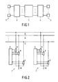
- the principle of an asynchronous time multiple transmission system can be explained with the block diagram shown in FIG. 1.
- the signals from a terminal for example telephone, video or audio signals, are segmented in a packetizer and provided with a header field in which a path identifier is present.
- the route identification contains information about the destination of the signals.
- Such a terminal and the packetizer form a subscriber terminal device 1.
- the data of such a terminal are thereby within successive time intervals (Time frame) transmitted in the form of cells.
- the duration of such a time frame depends on the underlying clock frequency of a transmission component.
- Such cells consist of the header field mentioned above and the useful information. If no data is to be transmitted within a time frame, an empty cell is formed, ie a cell in which it is indicated in the header that no further information follows.
- the data are transmitted, for example, from 64 subscriber terminals 1 to a line trunk group 2 via 64 lines, each with a capacity of 150 Mbit / s.
- connection group 2 the data are summarized and transmitted over a smaller number of lines with a higher capacity. For example, this data can be carried over 16 lines with a capacity of 600 Mbit / s each.
- a subsequent switching matrix 3 which is composed of several switching matrix blocks and each of these consists of several switching elements, the data is conveyed by evaluating the route identification by placing it on a specific customer line.
- a coupling element consists of a circuit arrangement which is connected to several feeder lines and one customer line.
- the circuit arrangement or the coupling element can determine data which are forwarded to the customer line connected to the coupling element and create the necessary paths within the circuit arrangement for this.
- the switching matrix 3 is again connected to a line group 4 with several lines, for example 16 lines, with a capacity of 600 Mbit / s.
- the line group 4 forwards the received data via lines to subscriber terminals 5. For example, there are 64 lines with a capacity of 150 Mbit / s provided.
- Such a system processes the data bidirectionally, ie this data is also transmitted from the subscriber terminal 5 to the subscriber terminal 1.
- a coupling element 7 is connected to a plurality of feeder lines 6.
- Each coupling element contains several crossing point circuits 8, each of which is connected to a feeder line 6.
- a crossover buffer for storing incoming cells is contained in the crossover point circuits 8.
- the readout process from the crossing buffers onto a customer line 10 is controlled in a coupling element by an allocation circuit 9.
- the assignment circuit 9 controls the reading order of the cells from the cross point circuits 8 to the pickup line 10 so that the cells are read out in the same order as they were read in. If several cells have arrived on different feeder lines at the same time, the cells are placed on the customer line 10 in a predetermined sequence.
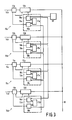
- FIG. 3 An embodiment of a coupling element according to the invention is shown in Fig. 3.
- this coupling element contains four crossing point circuits 15a to 15d.
- a coupling element can consist of further crossing point circuits.
- Each crossing point circuit 15a to 15d which is connected to a feeder line 14a to 14d, contains a cell filter 11a to 11d, a crossing buffer 12a to 12d and an assignment element 13a to 13d.
- the input of each cell filter 11a to 11d is connected to a feed line 14a to 14d.
- a Such a cell filter 11a to 11d checks whether the cell that has arrived should be put on the customer line 10.
- Each cell filter 11a to 11d can comprise, for example, a register, a comparator and a memory.
- a cell is read into the register.
- the path identifier of the cell stored in the register is fed to the comparator via a line and information from the memory is fed via a further line.
- the comparator uses the route identifier and the information from the memory to determine whether the route identifier is assigned to the customer line 10.
- intersection circuit 15a to 15d The structure of an intersection circuit 15a to 15d will be explained using the intersection circuit 15b. If the cell arriving in the cell filter 11b is to be read in the crossing buffer 12b connected to the cell filter 11b, a read signal is fed to the crossing buffer 12b via a control line, whereupon the cell is read into the crossing buffer 12b via a further line. An assignment element 13b is assigned to the crossing buffer 12b and controls the readout process from the crossing buffer 12b via a control line. The output of the crossing buffer 12b is connected to the customer line 10.
- the other crossing point circuits 15a, 15c and 15d have the same structure.
- An assignment element 13a to 13d each contains a read-out control 16a to 16d, a control buffer 17a to 17d and a read-in control 18a to 18d.
- the structure of an assignment element will be explained using the assignment element 13b.
- the control buffer 17b is connected to the read-in controller 18b via a data and control line and to the read-out controller 16b via a data and control line. Furthermore, the read-in controller 18b is connected to a cell filter 11b via a control line.
- a cell request circuit 19 is connected to the readout control 16a and this to the readout control 16b. There is also a connection between the readout controls 16b and 16c and between the readout controls 16c and 16d.
- the assignment elements 13a to 13d form an assignment circuit 9.
- the individual assignment elements 13a to 13d are structured hierarchically. The lowest assignment element in the hierarchy is the assignment element 13a, while the highest assignment element in the hierarchy is the assignment element 13d. If a cell arrives in the cell filter 11c, for example, which is assigned to the customer line 10, a signal is generated by the cell filter 11c, as a result of which the associated read-in controller 18c is informed that a cell has arrived. The read-in controller 18c then generates a binary one, which is read into the control buffer 17c.
- the read-in controller 18c generates an arrival signal, as a result of which the read-in controller 18b of the hierarchically lower assignment element 13b is informed that a cell has been read in the crossing buffer 12c.
- the read-in controller 18b then generates a binary zero which is read into the assigned control buffer 17b.
- the arrival signal is passed on by the read-in control 18b to the read-in control 18a, which also generates a binary zero which is read into the assigned control buffer 17a.
- the reading out of a cell from an intersection buffer 12a to 12d is controlled as follows: At the beginning of a time frame, the cell request circuit 19 generates an enable signal which is fed to the readout control 16a.
- the readout control 16a checks which state is present first in the control buffer 17a. If the readout control 16a determines that a binary one is stored in the control buffer 17a, a readout signal is generated by the readout control 16a for the crossing buffer 12a. Then a cell stored in the crossing buffer 12a is put on the pickup line 10. If a binary zero is stored in the control buffer 17a, the read-out control 16a forwards the release signal to the read-out control 16b of the hierarchically higher assignment element 13b.
- a binary one or a binary zero is present in the assigned control buffer 17b. If a binary one is present, a cell is output from the crossing buffer 12b by a read signal from the read controller 16b. If there is a binary zero in the control buffer 17b, the enable signal is passed on to the assignment element 13c. This chain is worked through to the last assignment element 13d.
- the cells must be read from a control buffer 12a to 12c for example, by delay elements not shown here or by a corresponding control of the reading from the control buffers 12a to 12c. This is because the evaluation of the release signal in the readout controls 16b to 16d gives rise to delays, which could result in overlapping cells if no delay is provided in the readout.
- control buffers 17a to 17d are filled when cells arrive on different feeder lines 14a to 14d. If, for example, a cell arrives on the feeder line 14a during a first time frame and is assigned to the customer line 10, only the read-in control 18a generates a binary one, which is stored in the control buffer 17a. It is assumed that a cell arrives on the feeder line 14d during a second time frame and is stored in the crossing buffer 12d. The read-in control 18d generates a binary one, which is stored in the control buffer 17d. Furthermore, the read-in control 18d generates an arrival signal which is passed on from the read-in control 18c to the read-in control 18a.
- each read-in control 18a to 18c After the arrival signal arrives, each read-in control 18a to 18c generates a binary zero, which is stored in the assigned control buffer 17a to 17c.
- cells assigned to the feeder line 10 are to arrive on the feeder lines 14a, 14b and 14d.
- a binary one is then stored in the control buffers 17a, 17b and 17d.
- An arrival signal is passed on by the read-in controller 18b to the read-in controller 18a, which then reads a binary zero into the control buffer 17a.
- the import control generates 18d an arrival signal, whereby a binary zero is read into the control buffers 17a to 17c. For example, during a fourth time frame, a cell arrives on the feeder line 14c.
- a binary one is then read into the control buffer 17c and a binary zero into the control buffers 17a and 17b. Finally, it should be assumed that a cell arrives only on the feeder line 14a during a fifth time frame. A read-in controller 18a then generates a binary one, which is read into the control buffer 17a.
- the binary states "1010001” are stored in the control buffer 17a, the binary states "0100” in the control buffer 17b, the binary states "001” in the control buffer 17c and the binary states "11” in the control buffer 17d .
- the cell request circuit 19 When reading out, after the cell request circuit 19 has supplied an enable signal to the readout control 16a, it is checked which state is present first in the control buffer 17a.
- the readout controller 16a determines that a binary one is stored in the control buffer 17a.
- the cell that arrived in the first time frame is then passed from the intersection buffer 12a to the customer line 10.
- the release signal After the release signal has been sent out by the cell request circuit 19 in the readout controller 16a, it is determined that a binary zero is present next in the control buffer 17a.
- the release signal is then supplied to the readout control 16b of the hierarchically higher assignment element. It is also found here that a binary zero is first stored in the control buffer 17b.
- the readout control 16c forwards the release signal to the readout control 16d. It is now determined here that there is a binary one in the control buffer 17d, whereupon the cell arriving on the feeder line 14d in the second time frame is passed on to the customer line 10. During the next time frame, the readout controller 16a determines that a binary one is next in the control buffer 17a, whereupon the cell arriving on the feeder line 14a in the third time frame is transferred to the customer line 10.
- the readout control 16a determines that a binary zero is present next in the control buffer 17a and then by the readout control 16b, that there is a binary one in the assigned control buffer 17b and that the next cell is output from the crossing buffer 12b.
- the respective readout controls 16a, 16b and 16c determine that a binary zero is present in their control buffers 17a to 17c.
- the enable signal thus arrives at the readout control 16d, which determines that a binary one is present in its assigned control buffer 17d.
- the cell which has arrived on the feeder line 14d in the third time frame is transferred to the customer line 10.
- the cells stored in the intersection buffers 12c and 12a are then added to the customer line 10.
Landscapes
- Engineering & Computer Science (AREA)
- Computer Networks & Wireless Communication (AREA)
- Signal Processing (AREA)
- Physics & Mathematics (AREA)
- Mathematical Physics (AREA)
- Data Exchanges In Wide-Area Networks (AREA)
Applications Claiming Priority (2)
| Application Number | Priority Date | Filing Date | Title |
|---|---|---|---|
| DE4012768 | 1990-04-21 | ||
| DE4012768A DE4012768A1 (de) | 1990-04-21 | 1990-04-21 | Koppelelement |
Publications (2)
| Publication Number | Publication Date |
|---|---|
| EP0454218A1 true EP0454218A1 (fr) | 1991-10-30 |
| EP0454218B1 EP0454218B1 (fr) | 1995-07-05 |
Family
ID=6404825
Family Applications (1)
| Application Number | Title | Priority Date | Filing Date |
|---|---|---|---|
| EP91200891A Expired - Lifetime EP0454218B1 (fr) | 1990-04-21 | 1991-04-16 | Système de transmission à division temporelle |
Country Status (4)
| Country | Link |
|---|---|
| US (1) | US5138612A (fr) |
| EP (1) | EP0454218B1 (fr) |
| JP (1) | JPH04229744A (fr) |
| DE (2) | DE4012768A1 (fr) |
Cited By (1)
| Publication number | Priority date | Publication date | Assignee | Title |
|---|---|---|---|---|
| EP0580085A3 (en) * | 1992-07-24 | 1995-12-20 | Sel Alcatel Ag | Level limit checking circuit |
Families Citing this family (5)
| Publication number | Priority date | Publication date | Assignee | Title |
|---|---|---|---|---|
| DE4010535A1 (de) * | 1990-04-02 | 1991-10-10 | Philips Patentverwaltung | Koppelelement fuer ein asynchrones zeitvielfachuebermittlungssystem |
| DE4027611A1 (de) * | 1990-08-31 | 1992-03-05 | Philips Patentverwaltung | Koppelfeld fuer ein asynchrones zeitvielfachuebermittlungssystem |
| JP2947628B2 (ja) * | 1991-03-11 | 1999-09-13 | 富士通株式会社 | スイッチ制御装置 |
| US5272696A (en) * | 1992-01-23 | 1993-12-21 | Northern Telecom Limited | ATM plane merging filter for ATM switches and the method thereof |
| FR2708817B1 (fr) * | 1993-07-30 | 1995-09-08 | Boyer Pierre | Systèmes d'allocation d'intervalle de temps et multiplexeurs pourvus d'un de ces systèmes d'allocation d'intervalle de temps. |
Citations (2)
| Publication number | Priority date | Publication date | Assignee | Title |
|---|---|---|---|---|
| EP0245996A2 (fr) * | 1986-05-14 | 1987-11-19 | Nortel Networks Corporation | Procédé et commutateur pour commuter des informations |
| EP0362723A2 (fr) * | 1988-10-01 | 1990-04-11 | Philips Patentverwaltung GmbH | Réseau pour système de commutation |
Family Cites Families (2)
| Publication number | Priority date | Publication date | Assignee | Title |
|---|---|---|---|---|
| DE3823878A1 (de) * | 1988-07-14 | 1990-01-18 | Philips Patentverwaltung | Koppelfeld fuer ein vermittlungssystem |
| JPH0758963B2 (ja) * | 1989-01-27 | 1995-06-21 | 日本電気株式会社 | セル交換装置 |
-
1990
- 1990-04-21 DE DE4012768A patent/DE4012768A1/de not_active Withdrawn
-
1991
- 1991-04-16 EP EP91200891A patent/EP0454218B1/fr not_active Expired - Lifetime
- 1991-04-16 DE DE59105903T patent/DE59105903D1/de not_active Expired - Fee Related
- 1991-04-18 JP JP3112144A patent/JPH04229744A/ja active Pending
- 1991-04-18 US US07/688,779 patent/US5138612A/en not_active Expired - Fee Related
Patent Citations (2)
| Publication number | Priority date | Publication date | Assignee | Title |
|---|---|---|---|---|
| EP0245996A2 (fr) * | 1986-05-14 | 1987-11-19 | Nortel Networks Corporation | Procédé et commutateur pour commuter des informations |
| EP0362723A2 (fr) * | 1988-10-01 | 1990-04-11 | Philips Patentverwaltung GmbH | Réseau pour système de commutation |
Cited By (1)
| Publication number | Priority date | Publication date | Assignee | Title |
|---|---|---|---|---|
| EP0580085A3 (en) * | 1992-07-24 | 1995-12-20 | Sel Alcatel Ag | Level limit checking circuit |
Also Published As
| Publication number | Publication date |
|---|---|
| DE59105903D1 (de) | 1995-08-10 |
| US5138612A (en) | 1992-08-11 |
| JPH04229744A (ja) | 1992-08-19 |
| DE4012768A1 (de) | 1991-10-24 |
| EP0454218B1 (fr) | 1995-07-05 |
Similar Documents
| Publication | Publication Date | Title |
|---|---|---|
| DE3786298T2 (de) | Verfahren und Schalter zum Vermitteln von Informationen. | |
| DE69214968T2 (de) | Vermittlungssystem mit einer Eingangsverteilstufe für zeitmarkierte Pakete und mit einer Ausgangsstufe für die Gewährleistung der richtigen Reihenfolge der Pakete | |
| DE69033231T2 (de) | Erweitbare Paketvermittlungsarchitektur | |
| EP0276776A2 (fr) | Réseau numérique de commutation pour la commutation en circuit et en paquet, et matrice de couplage correspondante | |
| EP0329005B1 (fr) | Procédé pour l'établissement de circuits virtuels à travers les commutateurs d'un dispositif de commutation à plusieurs étages | |
| EP0453607A1 (fr) | Méthode et dispositif pour réduire la perte de paquets d'information, transmis par un commutateur de paquets | |
| EP0351014B1 (fr) | Réseau de commutation pour système de commutation | |
| DE68920028T2 (de) | Verfahren und Vorrichtung zum Vielfachzugriff mit zyklischer Reservierung in einem Kommunikationssystem. | |
| EP0004307B1 (fr) | Procédé pour la réalisation de connexions en conférence dans un système de commutation temporelle MIC | |
| EP0289087A2 (fr) | Système de commutation par paquets | |
| EP0762716A2 (fr) | Méthode, système de communication et unité de conférence pour réaliser des conférences | |
| DE69227444T2 (de) | Einrichtung für die Erzeugung von Mehradresspaketen in einem Paketvermittlungssystem | |
| CH653783A5 (de) | Steuereinrichtung, insbesondere fuer fernsprechvermittlungsanlagen. | |
| EP0454218B1 (fr) | Système de transmission à division temporelle | |
| EP0121238B1 (fr) | Montage pour installations de télécommunication, en particulier pour centraux téléphoniques comprenant des processeurs d'informations et des dispositifs pour éviter des surcharges | |
| EP0443672B1 (fr) | Système à mode de transfert asynchrone | |
| EP0442581B1 (fr) | Système de communication asynchrone à division temporelle | |
| EP0173274B1 (fr) | Méthode et montage pour la réalisation et la maintenance d'une liaison à division temporelle à large bande | |
| DE68903986T2 (de) | Vermittlungssystem fuer leitungs- und/oder paketvermittelte nachrichtenuebertragungen. | |
| EP0414950B1 (fr) | Méthode de commutation des informations transmises distributivement sur plusieurs tranches de temps | |
| DE69110192T2 (de) | Vermittlungsmodul digitaler Datenpakete zur Zuweisung leerer Pakete an einen Koppelpunkt. | |
| DE3626870C2 (fr) | ||
| EP0474283A1 (fr) | Réseau de commutation à technique ATM (Asynchronous Transfer Mode) | |
| DE4122276C2 (de) | Hierarchisches Synchronisationsverfahren für ein digitales Kommunikationssystem | |
| EP0450725B1 (fr) | Système à multiplexage temporel asynchrone avec un réseau de commutation |
Legal Events
| Date | Code | Title | Description |
|---|---|---|---|
| PUAI | Public reference made under article 153(3) epc to a published international application that has entered the european phase |
Free format text: ORIGINAL CODE: 0009012 |
|
| AK | Designated contracting states |
Kind code of ref document: A1 Designated state(s): DE FR GB IT |
|
| 17P | Request for examination filed |
Effective date: 19920429 |
|
| 17Q | First examination report despatched |
Effective date: 19940217 |
|
| GRAA | (expected) grant |
Free format text: ORIGINAL CODE: 0009210 |
|
| AK | Designated contracting states |
Kind code of ref document: B1 Designated state(s): DE FR GB IT |
|
| REF | Corresponds to: |
Ref document number: 59105903 Country of ref document: DE Date of ref document: 19950810 |
|
| ITF | It: translation for a ep patent filed | ||
| ET | Fr: translation filed | ||
| GBT | Gb: translation of ep patent filed (gb section 77(6)(a)/1977) |
Effective date: 19951013 |
|
| PG25 | Lapsed in a contracting state [announced via postgrant information from national office to epo] |
Ref country code: GB Effective date: 19960416 |
|
| PLBE | No opposition filed within time limit |
Free format text: ORIGINAL CODE: 0009261 |
|
| STAA | Information on the status of an ep patent application or granted ep patent |
Free format text: STATUS: NO OPPOSITION FILED WITHIN TIME LIMIT |
|
| 26N | No opposition filed | ||
| GBPC | Gb: european patent ceased through non-payment of renewal fee |
Effective date: 19960416 |
|
| PG25 | Lapsed in a contracting state [announced via postgrant information from national office to epo] |
Ref country code: FR Effective date: 19961227 |
|
| PG25 | Lapsed in a contracting state [announced via postgrant information from national office to epo] |
Ref country code: DE Effective date: 19970101 |
|
| REG | Reference to a national code |
Ref country code: FR Ref legal event code: ST |
|
| PG25 | Lapsed in a contracting state [announced via postgrant information from national office to epo] |
Ref country code: IT Free format text: LAPSE BECAUSE OF NON-PAYMENT OF DUE FEES Effective date: 20050416 |