EP0454417A2 - Gerät zur Verarbeitung eines Fernsehsignals - Google Patents
Gerät zur Verarbeitung eines Fernsehsignals Download PDFInfo
- Publication number
- EP0454417A2 EP0454417A2 EP91303645A EP91303645A EP0454417A2 EP 0454417 A2 EP0454417 A2 EP 0454417A2 EP 91303645 A EP91303645 A EP 91303645A EP 91303645 A EP91303645 A EP 91303645A EP 0454417 A2 EP0454417 A2 EP 0454417A2
- Authority
- EP
- European Patent Office
- Prior art keywords
- coefficient
- image signals
- amplification
- level
- digital data
- Prior art date
- Legal status (The legal status is an assumption and is not a legal conclusion. Google has not performed a legal analysis and makes no representation as to the accuracy of the status listed.)
- Granted
Links
Images


Classifications
-
- H—ELECTRICITY
- H04—ELECTRIC COMMUNICATION TECHNIQUE
- H04N—PICTORIAL COMMUNICATION, e.g. TELEVISION
- H04N5/00—Details of television systems
- H04N5/44—Receiver circuitry for the reception of television signals according to analogue transmission standards
- H04N5/57—Control of contrast or brightness
-
- H—ELECTRICITY
- H04—ELECTRIC COMMUNICATION TECHNIQUE
- H04N—PICTORIAL COMMUNICATION, e.g. TELEVISION
- H04N9/00—Details of colour television systems
- H04N9/64—Circuits for processing colour signals
- H04N9/68—Circuits for processing colour signals for controlling the amplitude of colour signals, e.g. automatic chroma control circuits
Definitions
- the present invention relates to image signal processing apparatus which provides processing to image signals in order to adjust the image contrast in the display of pictures corresponding to image signals.
- the magnitude of a gain to the said image signal has been regulated, for example, irrespective of changes in the level of an input image signal. Therefore, once the contrast level is set, a specified gain is provided whether the level of the input image signal is high or low.
- Fig. 1 shows the basic structure to conduct the above conventional contrast adjustment.
- the input image signal A is amplified at the amplifier 1 according to the gain adjusted by the contrast control knob 2, i.e., the contrast level to be given as output image signal B.
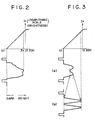
- Fig. 2 there exists such relationship as shown in Fig. 2 between the electric current (IK) of the cathode and the voltage (EGK) between the grid and the cathode of the braun tube (CRT) which is generally used to display pictures corresponding to image signals. Also, there is proportional relationship between the cathode current and brightness.
- the Ec in the Figure indicates a cut-off voltage, below which there is no glow of cathode current on the braun tube. Es is also the maximum permissible driving voltage, above which the cathode current becomes too large and the spot diameter of electron beam grows large resulting in the inability to show minute part of a picture and increase of X ray generated from the braun tube.
- the voltage applied to the braun tube should fall between Ec and Es.
- the range from Ec to Es is the dynamic range of the braun tube, which determines the contrast ratio of the braun tube (the ratio from black to white).
- the braun tube should be operated with the amplitude of image signal within this range in order to gain pictures having sufficient contrast.
- the image signals do not always move over the entire span of this range.
- the signal is located at a spot close to the black level indicated on (a) of Fig. 3, namely a small level of an image signal.
- the variable part of the signal as shown in (b) of Fig. 3, should be amplified and operated.
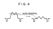
- a commercially variable method to utilize effectively the actuation range of the braun tube has been developed in which an autopedestal (Fig. 4) is given to lower automatically the level of pictoral signal corresponding to the most black part of the picture down to the pedestral level or the gain of the amplifier for image signals is raised (as in Fig. 3(b)) to utilize the full actuation range of the braun tube.
- This invention intends to provide the image signal processing apparatus which solves the above-mentioned problems.
- Other purpose of this invention is to provide the image signal processing equipment which allows the automatic contrast adjustment according to the level of image signals.
- the image signal processing apparatus as one embodiment of the present invention, comprising level distribution information generating means for generating information which indicates the level distribution condition of input image signals during a specified period of time and level control means for controlling levels of image signals according to information generated by the level distribution information generating means.
- the other purpose of the present invention is to provide image signal processing apparatus which is capable of making contrast adjustment most suitable for respective level of image signals.
- the image signal processing equipment as one embodiment of the present invention, comprising: conversion means for converting analogue image signal into digital data and output said digital data; detection and operation means for detecting and operating the maximum value, minimum value and intermediate value of the above digital data; coefficient calculation means for calculating the first coefficient based on the maximum, minimum and intermediate values detected and operated by said detection and operation means; coefficient generating means for generating the second coefficient; coefficient operating means for conducting operation using the first coefficient calculated by the coefficient calculating means and the second coefficient calculated by the coefficient generating means to calculate the third coefficient; and level control means for controlling the level of image signal using the third coefficient calculated by the coefficient operating means.
- Another objective of this invention is to provide image signal processing equipment which is capable of improving visual quality of picture.
- the image signal processing apparatus as one embodiment of the present invention comprising: conversion means for converting analogue image signal into digital data and output said digital signal; detection and operation means for detecting and operating the maximum, minimum and intermediate values of the above digital data and at the same time shift the level of the calculated intermediate value according to the level of the detected maximum or minimum values; coefficient calculation means for calculating the first coefficient on the basis of the maximum, minimum and intermediate values detected and operated by said detection and operation means; coefficient generation means for generating the second coefficient; coefficient operation means for operating and calculate the third coefficient using the first coefficient calculated by said coefficient calculation means and the second coefficient generated by said coefficient generation means; and level control means for controlling the level of the pictorial signal using the third coefficient calculated by said coefficient operation means.
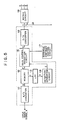
- Fig. 5 is a drawing showing an outlined structure of the contrast adjustment circuit as the first embodiments of the present invention.
- item 11 is an A/D converter
- item 12 is a field or frame memory
- item 13 is low-pass filter
- item 14 is a detection operation circuit
- item 15 is a gain control operation circuit
- item 16 is a D/A converter
- item 17 is an external contrast control circuit.
- the input image signal A is converted to the digital data B at the A/D converter 11.
- the digital data B is supplied to the digital data of the memory 12, in which the digital data corresponding to one screen (1 field or 1 frame volume) is stored.
- the digital data stored in the said memory is supplied to LPF13.
- the data, after the over-shoot and pre-shoot generated in the pictorial signal indicated on the digital data by said LPF3 are removed, are supplied to the detection/operation circuit 14.
- the detection and operation circuit 14 and the gain control circuit 15 have the structure shown in Fig. 6.
- the digital data output by the above LPF13 are supplied to the detection/operation unit 20 which is arranged to calculate the average value of the digital data corresponding to one screen (APL) accumulated in the above memory 12 using the supplied digital data and also detect the maximum value (WP) and the minimum value (DP) of the digital data corresponding to one screen which are stored in the above memory 12.
- the detection/operation part 20 determines the gain value of pictorial signal based on the following operation formula from the detected or operated avarage value (APL), the maximum value (WP), the minimum value (DP) and the threshold maximum value (W) and the threshold minimum value (D) of the image signal.
- APL detected or operated avarage value
- WP maximum value
- DP minimum value
- W threshold maximum value
- D threshold minimum value
- the above operation formula (1) is the formula to determine the gain value G1 in case the digital data value is larger than the average value (APL).
- the operation formula (2) is the formula to determine the gain value G2 is the formula to determine the gain value G2 in case the digital data value is smaller than the average value (APL).
- the gain values G1 and G2 are equal to or greater than 1.
- the calculated average value APL is supplied to the judgement part 26 within the gain control operation circuit 15 which will be explained later.
- the gain values G1 and G2 are supplied to the judgement part 21 within the detection/operation circuit 14.
- the judgement part 21 outputs a signal to select one of the gain adjustment parts 22, 23 and 24 which generate differing gain adjustment data according to the size of the gain values G1 and G2 supplied from the above detection/operation part 20.
- the judgement part 21 supplies the above selection signal to the gain adjustment part 22 and supplies, for example, the gain adjustment GA which indicates "O" from the gain adjustment part 22 to the judgment amplification part 25. If 1.2 ⁇ G1 and G2 ⁇ 3, the above selection signal is supplied to the gain adjustment part 23, the gain adjustment data GB which, for example, indicates "1.5” is supplied from the said gain adjustment part 23 to the judgment amplification part 25. Further, in case 3 ⁇ G1 and G3, the above selection signal is supplied to the gain adjustment part 24, and the gain adjustment data GC which, for example, indicates "3" is supplied from the gain adjustment part 24 to the judgement amplification part 25.
- Values for the gain adjustment data GA, GB and GC which are output from the gain adjustment parts 22, 23 and 24 can be set by the external contrast control circuit 17.
- the average value data APL output from the above-mentioned detection/operation part 20 is supplied also to the judgment part within the gain control operation circuit 15 as stated above.
- the judgement part 26 determines whether the digital data stored in the above memory 12 is larger or smaller than the said average value data APL and supplies the results to the judgment amplification part 25.
- the judgement amplification part 25 sets the amplification gain of judgement data supplied from the above judgement part 26 and of the digital data supplied from the above memory 12 according to the gain adjustment data GA, GB and GC supplied from the above gain adjustment parts 22, 23 and 24. And the said digital data are amplified according to the set amplification gain and the amplified digital data G is supplied to the D/A converter 16 of Fig. 5.
- the digital data supplied from the gain control operation circuit 15 are converted to the analogue image signal (luminance signal Y). Then, the luminance signal Y is output from the said D/A converter 16 and supplied to the matrix circuit 18 along with the color differential signals I and Q processed in a color signal processing circuit which is not shown on the drawing.
- the matrix circuit 18 forms RGB signals from the supplied luminance signal Y, color differential signals I and Q, which are then supplied to the display part, including the braun tube, which is not shown on the drawing.
- Fig. 7 shows the amplification processing of the above image signals according to the distribution condition of levels of input image signals.
- Fig. 7A shows the case in which the image signal shows ordinary brightness
- Fig. 7B is the case of dark situation
- Fig. 7C is the case of bright situation.
- the left-hand side shows the distribution condition of the level of input image signals
- the right-hand side indicates the distribution condition of the level of image signals after the amplification processing.
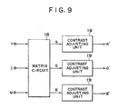
- contrast adjustment is made only about the luminance signal of image signals.
- the contrast adjustment part 19 having the same structure as in Fig. 5 is provided not only to the luminance signal Y but also to color differential signals I and Q to do the same processing, thereby conducting contrast adjustment most suitable for color picture receiving tube.
- the level control is given to the luminance signal Y, color differential signals I and Q for the purpose of contrast adjustment.
- matrix processing is done to the luminance signal Y and color differential signals I and Q, and after being converted to RGB signal, the contrast adjustment part 19 may be provided to each of the R (red), G (green) and B (blue) signals to make contrast adjustment.
- the dynamic range of the LC driving circuit is so narrow that the contrast adjustment by the structure shown in the embodiment is particularly effective, making it possible to restrict the phenomena of white collapse and black collapse leading to the display of contrast picture which is easy to see.
- Fig. 10 shows an outlined structure of the contrast adjustment circuit as the second embodiment of the present invention.
- the item 31 is an input terminal through which image signal is fed.
- the item 32 is an analogue/digital (A/D) converter is which after going through the low-pass filter (not shown on the drawing) to restrict the band in a specified area, the analogue image signal is subjected to sampling and quantizing and then converted into the digital data.
- the item 33 is a memory which memorizes and delays the digital data formed on the above A/D converter 32.
- Item 34 is a image processing circuit to do such processing as the multiplying of digital data by a coefficient.
- Item 35 is a digital/analogue (D/A) converter.
- Item 36 is a detection/operation circuit which detects the maximum value and the minimum value and calculate an intermediate value between the detected maximum value and minimum values.
- Item 37 is a coefficient calculation circuit to determine the amplification rate.
- Item 38 is a coefficient operation circuit which multiplies the coefficient calculated from item 37, a coefficient calculation circuit by the coefficient generated at item 39, a coefficient generation circuit.
- Item 39 is a coefficient generation circuit which generates a coefficient varying the amplification rate to obtain a desired contrast ratio.
- Item 40 is a control part which variably controls coefficients generated from item 39, the above coefficient generation circuit.
- the image signal input from the input terminal 31 is band-restricted through the low-pass filter (not shown on the drawing), which restricts bands in a desired band, and is then subjected to sampling (not shown on the drawing since the sampling clock generation circuit and power source are known) and quantizing at the A/D converter 32.
- the signals are converted into digital data, supplied to the memory circuit 33 one after another. For example, after data corresponding to one period of horizontal scanning are memorized, the signals are sent to the image processing circuit 34.
- the digital data output from the A/D converter 32 are supplied to the detection/operation circuit 36.
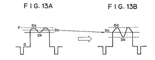
- the detection operation circuit 36 detects, from among digital data expressing effective image signals excluding synchronous part and pedestal part of image signals shown on Fig. 11, the maximum level data as the maximum value Da, the minimum level data as the minimum value Db, and the intermediate value Dc as to supply data to the coefficient calculation circuit 37.
- a detection operation circuit as Da, the minimum value as Db, the intermediate value as Dc, the maximum value of the possible digital data as F, the pedestal level as G and further Da - Db 2 as Dd the coefficient calculation curcuit 37 selects and outputs the smaller of F - Dc Dd and Dc - G Dd .
- this coefficient calculation circuit 37 is capable of obtaining the intermediate value of the image signals and then calculating the largest possible amplification rate without clipping the image signals.
- the coefficient generation circuit 39 generates a coefficient with which an operator varies the image contrast freely as desired. Thus, according to the indication data generated at the control part 40, a coefficient below is generated. If the coefficient value is 1, the contrast ratio is improved.
- the coefficient calculated at the coefficient calculation circuit 3 can extend from the minimum value of 1 to the maximum value close to infinity.
- the coefficient generated from the coefficient generation circuit 39 is below 1.
- the coefficient is input to the coefficient oepration circuit 38 to conduct the multiplication processing.
- the coefficient operation circuit 38 determines (or do limiter) the maximum value of the amplification rate (coefficient) which is to be set. For example, if the maximum value of the amplification rate (coefficient) is 2, the signal in Fig. 12A does not become a signal of Fig. 12B but is comparable to that of Fig. 12C, not leading to visual uncomfortableness.
- the coefficient value generated from the coefficient generation circuit 39 the coefficient calculated in the coefficient operation circuit 38 is more than 1 and lower than 2, then being supplied to the image processing circuit 34.
- the intermediate value obtained by the detection/operation circuit 36 is multiplied by the coefficient (amplification rate) obtained in the coefficient operation circuit 38 to conduct digital data processing as shown in Fig. 11B.
- the digital data processed in the image processing circuit are converted to analogue signals at the D/A converter 35 and, after being subjected to the band restriction in the low-pass filter shown on the drawing, are supplied to the driving circuit of the braun tube shown on the drawing.
- the maximum value and the minimum value of image signals are detected by digitalizing the image signals. Further, by obtaining the intermediate value and structuring to vary the gain coefficient of image signals according to the said intermediate value, the picture corresponding to the image signal can be displayed with sufficient contrast with substantially improved quality of picture.
- the contrast is improved by moving the intermediate value Dc.
- the moving amount of the intermediate value Dc in this case should be 15 - 20 % so that there may be no sense of incongruity visually.
- the contrast is improved as shown in Fig. 13B by shifting the level of intermediate value or doing white elongation or black elongation with respect to signals which have a small contrast ratio at a place close to white peak or black level.
- the term "average” above encompasses not only the arithmetic mean, but also any other measure giving a representative signal value (for example, the median value, or the geometric mean, or the sum).
- the average may be derived from the output of the low pass filter 13, and hence represent the low pass filtered average.
- the low pass filter 13 may, for example, be arranged to smooth out sudden peak white or peak black pixel values due to, for example, noise.
- the average may alternatively be derived to omit such isolated peak values from the calculation of the average.
Landscapes
- Engineering & Computer Science (AREA)
- Multimedia (AREA)
- Signal Processing (AREA)
- Television Receiver Circuits (AREA)
- Controls And Circuits For Display Device (AREA)
- Picture Signal Circuits (AREA)
Applications Claiming Priority (6)
| Application Number | Priority Date | Filing Date | Title |
|---|---|---|---|
| JP114595/90 | 1990-04-26 | ||
| JP11459590A JPH048069A (ja) | 1990-04-26 | 1990-04-26 | デジタル画像処理回路 |
| JP114592/90 | 1990-04-26 | ||
| JP11459290A JPH048068A (ja) | 1990-04-26 | 1990-04-26 | デジタル画像処理回路 |
| JP11196290A JP2832066B2 (ja) | 1990-04-27 | 1990-04-27 | コントラスト調整装置 |
| JP111962/90 | 1990-04-27 |
Publications (3)
| Publication Number | Publication Date |
|---|---|
| EP0454417A2 true EP0454417A2 (de) | 1991-10-30 |
| EP0454417A3 EP0454417A3 (en) | 1992-03-04 |
| EP0454417B1 EP0454417B1 (de) | 1997-09-03 |
Family
ID=27312137
Family Applications (1)
| Application Number | Title | Priority Date | Filing Date |
|---|---|---|---|
| EP91303645A Expired - Lifetime EP0454417B1 (de) | 1990-04-26 | 1991-04-23 | Gerät zur Verarbeitung eines Fernsehsignals |
Country Status (4)
| Country | Link |
|---|---|
| US (1) | US5210610A (de) |
| EP (1) | EP0454417B1 (de) |
| CA (1) | CA2040672C (de) |
| DE (1) | DE69127493T2 (de) |
Cited By (8)
| Publication number | Priority date | Publication date | Assignee | Title |
|---|---|---|---|---|
| EP0554938A1 (de) * | 1992-02-04 | 1993-08-11 | Philips Patentverwaltung GmbH | Verfahren zur Kontrastkorrektur |
| EP0599398A3 (en) * | 1992-11-24 | 1994-06-22 | Philips Patentverwaltung | Video signal processing circuit. |
| WO1995033332A3 (en) * | 1994-06-01 | 1996-01-18 | Simage Oy | Imaging devices, systems and methods |
| EP0963111A1 (de) * | 1998-06-02 | 1999-12-08 | Deutsche Thomson-Brandt Gmbh | Verfahren und Vorrichtung zur dynamischen Kontrastverbesserung in Videobildern |
| EP0963112A1 (de) * | 1998-06-02 | 1999-12-08 | Deutsche Thomson-Brandt Gmbh | Verfahren und Vorrichtung zur dynamischen Kontrastverbesserung in Videobildern |
| US6035013A (en) * | 1994-06-01 | 2000-03-07 | Simage O.Y. | Radiographic imaging devices, systems and methods |
| EP1070424A4 (de) * | 1998-03-14 | 2003-06-04 | Nuwave Technologies Inc | Bildkorrektursgerät mit vbi information |
| EP2670145A1 (de) * | 2012-05-31 | 2013-12-04 | Kabushiki Kaisha Toshiba | Videoverarbeitungsvorrichtung und Verfahren zur Verarbeitung von Videos |
Families Citing this family (15)
| Publication number | Priority date | Publication date | Assignee | Title |
|---|---|---|---|---|
| US5451948A (en) * | 1994-02-28 | 1995-09-19 | Cubic Communications, Inc. | Apparatus and method for combining analog and digital automatic gain control in receivers with digital signal processing |
| US5446503A (en) * | 1994-04-11 | 1995-08-29 | Mitsubishi Semiconductor America, Inc. | Vertical detail enhancement with stepped return coring |
| JP3685575B2 (ja) * | 1997-01-30 | 2005-08-17 | 三菱電機株式会社 | ディスプレイ装置 |
| US6337676B1 (en) * | 1998-03-30 | 2002-01-08 | Kabushiki Kaisha Toshiba | Flat-panel display device |
| TWI285872B (en) * | 1999-05-10 | 2007-08-21 | Matsushita Electric Industrial Co Ltd | Image display device and method for displaying image |
| JP3649043B2 (ja) * | 1999-06-07 | 2005-05-18 | セイコーエプソン株式会社 | 画像表示装置及び方法、並びに、画像処理装置及び方法 |
| EP1075140A1 (de) * | 1999-08-02 | 2001-02-07 | Koninklijke Philips Electronics N.V. | Verbesserung eines Videosignals |
| JP3741212B2 (ja) * | 2001-07-26 | 2006-02-01 | セイコーエプソン株式会社 | 画像処理システム、プロジェクタ、プログラム、情報記憶媒体および白黒伸張処理方法 |
| JP3838177B2 (ja) * | 2002-08-22 | 2006-10-25 | 株式会社日立製作所 | 映像表示方法、映像表示装置及びそれに用いるコントラスト調整回路 |
| JP4927311B2 (ja) * | 2003-08-27 | 2012-05-09 | 株式会社日立製作所 | 映像表示装置、それに用いる表示部駆動回路及び映像表示方法 |
| US8207931B2 (en) * | 2007-05-31 | 2012-06-26 | Hong Kong Applied Science and Technology Research Institute Company Limited | Method of displaying a low dynamic range image in a high dynamic range |
| JP4977573B2 (ja) * | 2007-10-11 | 2012-07-18 | オンセミコンダクター・トレーディング・リミテッド | 映像信号処理装置におけるオートゲインコントロール回路 |
| TWI387335B (zh) * | 2008-05-26 | 2013-02-21 | Novatek Microelectronics Corp | 信號調節電路及其視訊裝置 |
| EP2769540B1 (de) | 2011-10-20 | 2018-11-28 | Dolby Laboratories Licensing Corporation | Verfahren und system zur entzerrung von videoinhalten |
| US9008458B2 (en) | 2013-02-07 | 2015-04-14 | Raytheon Company | Local area processing using packed distribution functions |
Family Cites Families (13)
| Publication number | Priority date | Publication date | Assignee | Title |
|---|---|---|---|---|
| US3790706A (en) * | 1972-05-25 | 1974-02-05 | Boeing Co | Automatic video contrast control circuit |
| US4187519A (en) * | 1978-08-17 | 1980-02-05 | Rockwell International Corporation | System for expanding the video contrast of an image |
| US4231065A (en) * | 1979-01-11 | 1980-10-28 | Honeywell Inc. | Local area contrast enhancement device |
| FR2456448A1 (fr) * | 1979-05-11 | 1980-12-05 | Thomson Csf | Dispositif de commande automatique de la fonction de transfert d'un systeme de transmission videofrequence en vue d'ameliorer la perception des images |
| JPS56107674A (en) * | 1980-01-31 | 1981-08-26 | Sony Corp | Gradation correcting device of video signal |
| US4470067A (en) * | 1980-12-27 | 1984-09-04 | Japan Broadcasting Corp. | Automatic gain control apparatus |
| FR2506549A1 (fr) * | 1981-05-22 | 1982-11-26 | Thomson Csf | Dispositif de correction des informations couleur fournies par les tubes analyseurs d'une camera en vue d'ameliorer la perception des images |
| JPS59125176A (ja) * | 1982-12-30 | 1984-07-19 | インタ−ナシヨナル ビジネス マシ−ンズ コ−ポレ−シヨン | ビデオイメ−ジのシエ−ジング効果の補正装置 |
| JPS59163953A (ja) * | 1983-03-08 | 1984-09-17 | Canon Inc | 画像処理装置 |
| US4731662A (en) * | 1985-03-21 | 1988-03-15 | Canon Kabushiki Kaisha | Image processing method for processing an image signal differently depending on the range of an image characteristic thereof relative to the range within which an output device can reproduce the image characteristic |
| FR2581775B1 (fr) * | 1985-05-10 | 1990-03-23 | Thomson Cgr | Procede de reglage de l'echelle des gris dans la reproduction d'images numerisees et systeme mettant en oeuvre ce procede |
| FR2604841B1 (fr) * | 1986-10-07 | 1988-11-25 | Etude Signal | Dispositif de transformation d'un signal par stabilisation et rehaussement de la dynamique dudit signal |
| DE3714861A1 (de) * | 1987-05-05 | 1988-11-24 | Fraunhofer Ges Forschung | Verfahren und vorrichtung zur aufbereitung von videosignalen |
-
1991
- 1991-04-17 CA CA002040672A patent/CA2040672C/en not_active Expired - Lifetime
- 1991-04-18 US US07/687,454 patent/US5210610A/en not_active Expired - Lifetime
- 1991-04-23 EP EP91303645A patent/EP0454417B1/de not_active Expired - Lifetime
- 1991-04-23 DE DE69127493T patent/DE69127493T2/de not_active Expired - Fee Related
Cited By (11)
| Publication number | Priority date | Publication date | Assignee | Title |
|---|---|---|---|---|
| EP0554938A1 (de) * | 1992-02-04 | 1993-08-11 | Philips Patentverwaltung GmbH | Verfahren zur Kontrastkorrektur |
| EP0599398A3 (en) * | 1992-11-24 | 1994-06-22 | Philips Patentverwaltung | Video signal processing circuit. |
| WO1995033332A3 (en) * | 1994-06-01 | 1996-01-18 | Simage Oy | Imaging devices, systems and methods |
| US5812191A (en) * | 1994-06-01 | 1998-09-22 | Simage Oy | Semiconductor high-energy radiation imaging device |
| US6035013A (en) * | 1994-06-01 | 2000-03-07 | Simage O.Y. | Radiographic imaging devices, systems and methods |
| EP1070424A4 (de) * | 1998-03-14 | 2003-06-04 | Nuwave Technologies Inc | Bildkorrektursgerät mit vbi information |
| EP0963111A1 (de) * | 1998-06-02 | 1999-12-08 | Deutsche Thomson-Brandt Gmbh | Verfahren und Vorrichtung zur dynamischen Kontrastverbesserung in Videobildern |
| EP0963112A1 (de) * | 1998-06-02 | 1999-12-08 | Deutsche Thomson-Brandt Gmbh | Verfahren und Vorrichtung zur dynamischen Kontrastverbesserung in Videobildern |
| US6285413B1 (en) | 1998-06-02 | 2001-09-04 | Deutsche Thomson-Brandt Gmbh | Method and apparatus for dynamic contrast improvement in video pictures |
| EP2670145A1 (de) * | 2012-05-31 | 2013-12-04 | Kabushiki Kaisha Toshiba | Videoverarbeitungsvorrichtung und Verfahren zur Verarbeitung von Videos |
| US8704953B2 (en) | 2012-05-31 | 2014-04-22 | Kabushiki Kaisha Toshiba | Video processing device and method of video processing |
Also Published As
| Publication number | Publication date |
|---|---|
| DE69127493D1 (de) | 1997-10-09 |
| US5210610A (en) | 1993-05-11 |
| CA2040672C (en) | 1995-05-30 |
| EP0454417B1 (de) | 1997-09-03 |
| DE69127493T2 (de) | 1998-01-08 |
| EP0454417A3 (en) | 1992-03-04 |
Similar Documents
| Publication | Publication Date | Title |
|---|---|---|
| EP0454417B1 (de) | Gerät zur Verarbeitung eines Fernsehsignals | |
| JP4271978B2 (ja) | 映像表示装置 | |
| KR100512542B1 (ko) | 비디오신호의화질보정회로 | |
| DE69225263T2 (de) | Gradationskorrekturanordnung | |
| JP3215388B2 (ja) | 画像表示装置および画像表示方法 | |
| JP3430998B2 (ja) | 画像表示装置および画像表示方法 | |
| EP0966165A1 (de) | Videosignalverarbeitungsschaltung mit optimalem Signalpegel für invertierte Gammakorrektur | |
| EP1372340B1 (de) | Verfahren und Vorrichtung zur dynamischen Kontrastverbesserung in Videobildern | |
| US6822695B2 (en) | Surrounding light judging method and video compensation control apparatus using the same | |
| EP0963111A1 (de) | Verfahren und Vorrichtung zur dynamischen Kontrastverbesserung in Videobildern | |
| US20030222841A1 (en) | Signal processing unit and liquid crystal display device | |
| US7110046B2 (en) | Method for dynamically adjusting video brightness | |
| US20060215925A1 (en) | Image processing device, image processing program, image processing method, and electronic camera for controlling degree of noise reduction in image data | |
| JP4333163B2 (ja) | 画像処理装置および画像表示装置、並びに画像処理方法 | |
| JP3215399B1 (ja) | 画像表示装置および画像表示方法 | |
| JP3208814B2 (ja) | 映像信号補正装置 | |
| US7719619B2 (en) | Image processing apparatus | |
| JP4175024B2 (ja) | 画像表示装置および画像処理装置、並びに画像処理方法 | |
| JPH11305734A (ja) | 液晶表示装置 | |
| US5502508A (en) | Gradation compensating apparatus for a video signal | |
| JPH0690382A (ja) | 階調補正装置 | |
| KR20100004329A (ko) | 어두운 영역의 화질 개선장치 | |
| JP2832066B2 (ja) | コントラスト調整装置 | |
| JP4085285B2 (ja) | フラットパネルディスプレイ型テレビジョン受信機、および、パネル用信号生成装置 | |
| JPH06326942A (ja) | 電子ディスプレイの制御方法およびその装置 |
Legal Events
| Date | Code | Title | Description |
|---|---|---|---|
| PUAI | Public reference made under article 153(3) epc to a published international application that has entered the european phase |
Free format text: ORIGINAL CODE: 0009012 |
|
| AK | Designated contracting states |
Kind code of ref document: A2 Designated state(s): DE FR GB IT NL |
|
| PUAL | Search report despatched |
Free format text: ORIGINAL CODE: 0009013 |
|
| AK | Designated contracting states |
Kind code of ref document: A3 Designated state(s): DE FR GB IT NL |
|
| 17P | Request for examination filed |
Effective date: 19920723 |
|
| 17Q | First examination report despatched |
Effective date: 19941125 |
|
| GRAG | Despatch of communication of intention to grant |
Free format text: ORIGINAL CODE: EPIDOS AGRA |
|
| GRAH | Despatch of communication of intention to grant a patent |
Free format text: ORIGINAL CODE: EPIDOS IGRA |
|
| GRAH | Despatch of communication of intention to grant a patent |
Free format text: ORIGINAL CODE: EPIDOS IGRA |
|
| GRAA | (expected) grant |
Free format text: ORIGINAL CODE: 0009210 |
|
| AK | Designated contracting states |
Kind code of ref document: B1 Designated state(s): DE FR GB IT NL |
|
| REF | Corresponds to: |
Ref document number: 69127493 Country of ref document: DE Date of ref document: 19971009 |
|
| ET | Fr: translation filed | ||
| ITF | It: translation for a ep patent filed | ||
| PLBE | No opposition filed within time limit |
Free format text: ORIGINAL CODE: 0009261 |
|
| STAA | Information on the status of an ep patent application or granted ep patent |
Free format text: STATUS: NO OPPOSITION FILED WITHIN TIME LIMIT |
|
| 26N | No opposition filed | ||
| REG | Reference to a national code |
Ref country code: GB Ref legal event code: IF02 |
|
| PGFP | Annual fee paid to national office [announced via postgrant information from national office to epo] |
Ref country code: NL Payment date: 20090427 Year of fee payment: 19 Ref country code: DE Payment date: 20090430 Year of fee payment: 19 Ref country code: FR Payment date: 20090424 Year of fee payment: 19 Ref country code: IT Payment date: 20090417 Year of fee payment: 19 |
|
| PGFP | Annual fee paid to national office [announced via postgrant information from national office to epo] |
Ref country code: GB Payment date: 20090428 Year of fee payment: 19 |
|
| REG | Reference to a national code |
Ref country code: NL Ref legal event code: V1 Effective date: 20101101 |
|
| GBPC | Gb: european patent ceased through non-payment of renewal fee |
Effective date: 20100423 |
|
| REG | Reference to a national code |
Ref country code: FR Ref legal event code: ST Effective date: 20101230 |
|
| PG25 | Lapsed in a contracting state [announced via postgrant information from national office to epo] |
Ref country code: NL Free format text: LAPSE BECAUSE OF NON-PAYMENT OF DUE FEES Effective date: 20101101 |
|
| PG25 | Lapsed in a contracting state [announced via postgrant information from national office to epo] |
Ref country code: DE Free format text: LAPSE BECAUSE OF NON-PAYMENT OF DUE FEES Effective date: 20101103 |
|
| PG25 | Lapsed in a contracting state [announced via postgrant information from national office to epo] |
Ref country code: IT Free format text: LAPSE BECAUSE OF NON-PAYMENT OF DUE FEES Effective date: 20100423 Ref country code: GB Free format text: LAPSE BECAUSE OF NON-PAYMENT OF DUE FEES Effective date: 20100423 |
|
| PG25 | Lapsed in a contracting state [announced via postgrant information from national office to epo] |
Ref country code: FR Free format text: LAPSE BECAUSE OF NON-PAYMENT OF DUE FEES Effective date: 20100430 |