EP0454467A1 - Datenübertragung und Datensammlung durch Verwendung eines matrixförmig verdrahteten Mediums - Google Patents
Datenübertragung und Datensammlung durch Verwendung eines matrixförmig verdrahteten Mediums Download PDFInfo
- Publication number
- EP0454467A1 EP0454467A1 EP91303764A EP91303764A EP0454467A1 EP 0454467 A1 EP0454467 A1 EP 0454467A1 EP 91303764 A EP91303764 A EP 91303764A EP 91303764 A EP91303764 A EP 91303764A EP 0454467 A1 EP0454467 A1 EP 0454467A1
- Authority
- EP
- European Patent Office
- Prior art keywords
- wires
- group
- slave
- data
- current flow
- Prior art date
- Legal status (The legal status is an assumption and is not a legal conclusion. Google has not performed a legal analysis and makes no representation as to the accuracy of the status listed.)
- Withdrawn
Links
Images


Classifications
-
- H—ELECTRICITY
- H04—ELECTRIC COMMUNICATION TECHNIQUE
- H04Q—SELECTING
- H04Q9/00—Arrangements in telecontrol or telemetry systems for selectively calling a substation from a main station, in which substation desired apparatus is selected for applying a control signal thereto or for obtaining measured values therefrom
Definitions
- This invention relates to the electrical transmission of data between a large number of slave stations and a single master station, using a matrixed wire medium that is particularly appropriate for a total system extent of a few metres.
- a method and apparatus for bi-directional data transmission employing a first group of m wires and a second group of n wires arranged as a matrix with m x n crosspoints, also employing a plurality of slave stations each connected between one wire of the first group and one wire of the second group at one of said crosspoints and having a resistance value that is coded to represent data that is to be transmitted from said slave station, and also employing a master station arranged firstly to allow current flow in only one of said first groups of wires and secondly to complete the path for said current flow sequentially via one or a plurality of said second groups of wires so as to address by current flow one or a plurality of said slave stations and thirdly to measure the voltage between, or the current flowing through, a pair of wires one from each of said first and second groups, so as to allow the value of resistance of each addressed slave station to be interpreted by said master station, and fourthly to modulate said current flow in intensity or duration so as to transmit data from
- the invention provides the advantages of high speed collection of variable amounts of data from a large number or sources, without requiring expensive terminal equipment or incurring any protocol overhead.
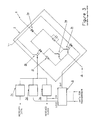
- Figure 1 shows in outline schematic a wire matrix and master and slave units.
- FIG. 2 shows in schematic form details of the master unit.
- FIG. 3 shows in schematic form details of a slave unit.
- Figure 1 illustrates the known principles of matrix selection, and provides a reference for the following description of the present invention.
- a first group of m wires 1 and a second group of n wires 2 are arranged so that up to m x n slave stations may be connected between one wire of the first group and one wire of the second group.
- the slave station 3 has its positive terminal 4 connected to the first wire of the second group and its negative terminal 5 connected to the first wire of the first group 1.
- the master station 6 selects an individual slave station by connecting one wire of the first group to a positive electrical source and one wire of the second group to a negative electrical sink.
- FIG. 2 shows details of the master station 6 of the present invention.
- a microprocessor 6a controls the matrix addressing and the transmission and reception of data, and passes this data to the user via ports 6b and 6c .
- the second group of wires may also be addressed one-at-a-time, but may advantageously be addressed several-at-a-time to increase the overall rate at which data may be transmitted.
- the port 6g may comprise n wires so that the microprocessor 6a has complete control over the addressing mode.
- Each member of the second group of wires is selected by the setting of a low level on the appropriate output of latch 6h .
- the resistor-transistor combination such as 6i for wire 1 will then establish a defined selection current from the positive supply pole which will pass through the addressed slave station and return via a transistor switch such as 6f .
- the programme of microprocessor 6a may send '0' or '1' bits to the addressed slave by generating short or long selection pulses, and a stream of such pulses may be sent to form a byte of information.
- the decoding of such data will be described later with reference to figure 3. It will be evident that analogue or digital information might also be sent to the slave station by varying the magnitude of the selection current.
- Data from the slave station may be represented by varying voltage-drop across the elements of the slave. This voltage drop may be classified as representing '0' or '1' by a signal-conditioning comparator such as 6j and presented to the microprocessor via port 6k . It will be evident that analogue information might be received from the slave station by substituting an analogue-to-digital converter for the comparator at 6j , and that the data returned during a stream of selection pulses might represent a digital byte or a series of different analogue signals.
- Figure 3 shows details of a slave station 3 of the present invention.
- a principal series connected circuit comprising blocking diode 3a which is a common feature of matrix circuits serving to prevent the spurious energisation of three slave stations in series, receiving opto-coupler 3b which responds to the current from the master station and provides a galvanically isolated signal to timing circuits 3c , 3d , and 3e , and resistor 3f which may be controllably shorted-out by switching transistor circuit 3g and opto-isolator 3h in response to digital data appearing at the output of shift-register 3i so as to transmit this data to the master station for conditioning as described in connection with 6j of figure 2.
- the timing circuit 3e is a negative-edge triggered monostable that signals the end of a selection pulse from the master. This is the correct time for the functional slave circuits to interpret the output of the positive level-triggered monostable 3c , which will still be low if the selection pulse was short, or high if it was long, thus decoding the data from the master station.
- the output of 3e also advances the data stored in shiftregister 3i , so that the next bit is presented via optocoupler 3h ready for the next selection pulse.
- the master station programme does not require further bits at this time, and instead addresses another slave unit, then the negative level monostable 3d will time out and cause the shift register 3i to reload in parallel mode with a new sample from the functional circuits of the slave.
- the master station thus has the flexibility to send and receive just one bit per slave station in one bit period, or a larger number of bits in a proportionally longer time, and so can adapt its addressing strategy according to the urgency of the information.
- the maximum bit rate is 100KBit per second per wire
- the microprocessor 6a of figure 2 is programmed to interleave a number of scanning strategies such as those just described, for example, so as to receive 1 bit from each slave unit frequently, to receive 8 bits less frequently and to transmit 1 bit even less frequently.
- a number of scanning strategies such as those just described, for example, so as to receive 1 bit from each slave unit frequently, to receive 8 bits less frequently and to transmit 1 bit even less frequently.
- the collection of 1 bit from all slave stations with a total scan time of 0.64 milliseconds might be followed by the sending of one bit to 2 slave stations in 0.04 milliseconds or less, and the collection of 8 bits from 4 slave stations in 0.32 milliseconds. This sequence would take up to 1 millisecond in total after which it might be repeated with the sending of 1 bit and the receiving of 8 bits from other slave stations.
- the overall effect would be to receive 1 bit from each slave station with a maxium delay of 1 millisecond, to send one bit to each slave station with a maximum delay of 256 milliseconds, and to receive 8 bits from each slave station with a maximum delay of 128 milliseconds.
Landscapes
- Engineering & Computer Science (AREA)
- Computer Networks & Wireless Communication (AREA)
- Selective Calling Equipment (AREA)
Applications Claiming Priority (2)
| Application Number | Priority Date | Filing Date | Title |
|---|---|---|---|
| GB9009556A GB2243473B (en) | 1990-04-27 | 1990-04-27 | Data transmission and collection using a matrixed wire medium |
| GB9009556 | 1990-04-27 |
Publications (1)
| Publication Number | Publication Date |
|---|---|
| EP0454467A1 true EP0454467A1 (de) | 1991-10-30 |
Family
ID=10675139
Family Applications (1)
| Application Number | Title | Priority Date | Filing Date |
|---|---|---|---|
| EP91303764A Withdrawn EP0454467A1 (de) | 1990-04-27 | 1991-04-25 | Datenübertragung und Datensammlung durch Verwendung eines matrixförmig verdrahteten Mediums |
Country Status (2)
| Country | Link |
|---|---|
| EP (1) | EP0454467A1 (de) |
| GB (1) | GB2243473B (de) |
Citations (4)
| Publication number | Priority date | Publication date | Assignee | Title |
|---|---|---|---|---|
| WO1985001168A1 (fr) * | 1983-09-05 | 1985-03-14 | Sony Corporation | Systeme de transmission de donnees |
| DE3613108A1 (de) * | 1986-04-18 | 1987-10-22 | Lumino Gmbh Licht Elektronik | Schaltungsanordnung zum gezielten ansteuern von funktionsmodulen ueber ein bus-system |
| EP0306934A2 (de) * | 1987-09-09 | 1989-03-15 | Willemin Electronic S.A. | Verfahren zur elektronischen Datenübertragung und Einrichtung zur Durchführung des Verfahrens |
| ES2009663A6 (es) * | 1988-10-31 | 1989-10-01 | Fornes Callis Juan | Aparato electronico periferico de ordenador para captura de senales de una red de sensores. |
Family Cites Families (1)
| Publication number | Priority date | Publication date | Assignee | Title |
|---|---|---|---|---|
| GB1361384A (en) * | 1971-07-27 | 1974-07-24 | Town R | Electrical arrangements for establishing electrical connection between a source and one of a plurality of remote units |
-
1990
- 1990-04-27 GB GB9009556A patent/GB2243473B/en not_active Expired - Fee Related
-
1991
- 1991-04-25 EP EP91303764A patent/EP0454467A1/de not_active Withdrawn
Patent Citations (4)
| Publication number | Priority date | Publication date | Assignee | Title |
|---|---|---|---|---|
| WO1985001168A1 (fr) * | 1983-09-05 | 1985-03-14 | Sony Corporation | Systeme de transmission de donnees |
| DE3613108A1 (de) * | 1986-04-18 | 1987-10-22 | Lumino Gmbh Licht Elektronik | Schaltungsanordnung zum gezielten ansteuern von funktionsmodulen ueber ein bus-system |
| EP0306934A2 (de) * | 1987-09-09 | 1989-03-15 | Willemin Electronic S.A. | Verfahren zur elektronischen Datenübertragung und Einrichtung zur Durchführung des Verfahrens |
| ES2009663A6 (es) * | 1988-10-31 | 1989-10-01 | Fornes Callis Juan | Aparato electronico periferico de ordenador para captura de senales de una red de sensores. |
Also Published As
| Publication number | Publication date |
|---|---|
| GB2243473B (en) | 1994-02-09 |
| GB9009556D0 (en) | 1990-06-20 |
| GB2243473A (en) | 1991-10-30 |
Similar Documents
| Publication | Publication Date | Title |
|---|---|---|
| CA1075791A (en) | Two-wire, multiple-transducer communications system | |
| CA1274304A (en) | Crosspoint circuitry for data packet space division switches | |
| US4326289A (en) | Expandable communication system | |
| GB2166328A (en) | In-house distribution facility for a broadband communication system | |
| KR870005524A (ko) | 스위치 노드 및 그 제어방법 | |
| ATE117148T1 (de) | Digitales signalübertragungssystem für die hausleittechnik. | |
| US5107260A (en) | Method and arrangement for transmitting data between a central data station and a plurality of data terminals in a local area network | |
| GB2135155A (en) | Switching system with separate supervisory links | |
| US4328586A (en) | Optically coupled serial communication bus | |
| EP0454467A1 (de) | Datenübertragung und Datensammlung durch Verwendung eines matrixförmig verdrahteten Mediums | |
| GB2130458A (en) | Asynchronous data transmission | |
| US2995626A (en) | Frequency signal telecommunication system | |
| US4503430A (en) | Apparatus for transmitting signals in a power driven textile machine | |
| GB2281475A (en) | Digital switching system interconnecting buses with incompatible protocols | |
| AU650969B2 (en) | Bidirectional data transmission | |
| SU1462505A1 (ru) | Телеграфна система св зи | |
| RU2250566C2 (ru) | Способ передачи электрических сигналов | |
| JPH03504664A (ja) | プロセツサユニツトのアドレツシング方法 | |
| SU930730A1 (ru) | Устройство дл передачи бипол рных телеграфных сигналов | |
| SU1141585A1 (ru) | Устройство дл передачи дискретных сигналов | |
| SU798777A1 (ru) | Система дл обмена информацией | |
| JPS5591009A (en) | Switching control unit | |
| SU1695355A1 (ru) | Адаптивный приемник телеметрической информации с рассредоточенных объектов | |
| SU1141435A1 (ru) | Устройство дл передачи телеизмерительной информации | |
| SU748403A1 (ru) | Устройство дл сопр жени телеграфных каналов с вычислительной машиной |
Legal Events
| Date | Code | Title | Description |
|---|---|---|---|
| PUAI | Public reference made under article 153(3) epc to a published international application that has entered the european phase |
Free format text: ORIGINAL CODE: 0009012 |
|
| AK | Designated contracting states |
Kind code of ref document: A1 Designated state(s): DE FR GB IT NL |
|
| STAA | Information on the status of an ep patent application or granted ep patent |
Free format text: STATUS: THE APPLICATION IS DEEMED TO BE WITHDRAWN |
|
| 18D | Application deemed to be withdrawn |
Effective date: 19920501 |