EP0454505A2 - Mehrwegübertragungssystem - Google Patents
Mehrwegübertragungssystem Download PDFInfo
- Publication number
- EP0454505A2 EP0454505A2 EP91303879A EP91303879A EP0454505A2 EP 0454505 A2 EP0454505 A2 EP 0454505A2 EP 91303879 A EP91303879 A EP 91303879A EP 91303879 A EP91303879 A EP 91303879A EP 0454505 A2 EP0454505 A2 EP 0454505A2
- Authority
- EP
- European Patent Office
- Prior art keywords
- signal transmission
- multiplex
- transmission lines
- signal
- voltage
- Prior art date
- Legal status (The legal status is an assumption and is not a legal conclusion. Google has not performed a legal analysis and makes no representation as to the accuracy of the status listed.)
- Granted
Links
Images


Classifications
-
- H—ELECTRICITY
- H04—ELECTRIC COMMUNICATION TECHNIQUE
- H04L—TRANSMISSION OF DIGITAL INFORMATION, e.g. TELEGRAPHIC COMMUNICATION
- H04L12/00—Data switching networks
- H04L12/28—Data switching networks characterised by path configuration, e.g. LAN [Local Area Networks] or WAN [Wide Area Networks]
-
- H—ELECTRICITY
- H04—ELECTRIC COMMUNICATION TECHNIQUE
- H04L—TRANSMISSION OF DIGITAL INFORMATION, e.g. TELEGRAPHIC COMMUNICATION
- H04L12/00—Data switching networks
- H04L12/28—Data switching networks characterised by path configuration, e.g. LAN [Local Area Networks] or WAN [Wide Area Networks]
- H04L12/40—Bus networks
- H04L12/40169—Flexible bus arrangements
- H04L12/40176—Flexible bus arrangements involving redundancy
- H04L12/40182—Flexible bus arrangements involving redundancy by using a plurality of communication lines
-
- H—ELECTRICITY
- H04—ELECTRIC COMMUNICATION TECHNIQUE
- H04L—TRANSMISSION OF DIGITAL INFORMATION, e.g. TELEGRAPHIC COMMUNICATION
- H04L12/00—Data switching networks
- H04L12/28—Data switching networks characterised by path configuration, e.g. LAN [Local Area Networks] or WAN [Wide Area Networks]
- H04L12/40—Bus networks
- H04L12/40006—Architecture of a communication node
- H04L12/40013—Details regarding a bus controller
-
- H—ELECTRICITY
- H04—ELECTRIC COMMUNICATION TECHNIQUE
- H04L—TRANSMISSION OF DIGITAL INFORMATION, e.g. TELEGRAPHIC COMMUNICATION
- H04L12/00—Data switching networks
- H04L12/28—Data switching networks characterised by path configuration, e.g. LAN [Local Area Networks] or WAN [Wide Area Networks]
- H04L12/40—Bus networks
- H04L12/407—Bus networks with decentralised control
- H04L12/413—Bus networks with decentralised control with random access, e.g. carrier-sense multiple-access with collision detection [CSMA-CD]
- H04L12/4135—Bus networks with decentralised control with random access, e.g. carrier-sense multiple-access with collision detection [CSMA-CD] using bit-wise arbitration
-
- H—ELECTRICITY
- H04—ELECTRIC COMMUNICATION TECHNIQUE
- H04L—TRANSMISSION OF DIGITAL INFORMATION, e.g. TELEGRAPHIC COMMUNICATION
- H04L25/00—Baseband systems
- H04L25/02—Details ; arrangements for supplying electrical power along data transmission lines
- H04L25/14—Channel dividing arrangements, i.e. in which a single bit stream is divided between several baseband channels and reassembled at the receiver
-
- H—ELECTRICITY
- H04—ELECTRIC COMMUNICATION TECHNIQUE
- H04L—TRANSMISSION OF DIGITAL INFORMATION, e.g. TELEGRAPHIC COMMUNICATION
- H04L12/00—Data switching networks
- H04L12/28—Data switching networks characterised by path configuration, e.g. LAN [Local Area Networks] or WAN [Wide Area Networks]
- H04L12/40—Bus networks
- H04L2012/40208—Bus networks characterized by the use of a particular bus standard
- H04L2012/40215—Controller Area Network CAN
Definitions
- This invention relates to a multipath transmission system for transmitting data among multiplex nodes connected to common signal transmission lines.
- This type of multipath transmission system includes a transmission system of a LAN (Local Area Network) utilizing a CSMA/CD (Carrier Senser Multiple Access/Collision Detection) with an NDA (Non Destructive Arbitration).
- a typical example of the LAN is a CAN (Controller Area Network) used for data transmission in cars, for example.
- terminal resistors R E , R E are connected to both ends of two signal transmission lines A and B and a plurality of multiplex nodes are connected in parallel with the signal transmission lines A and B.
- Each of the multiplex nodes is constructed by a communication control device, a transmission circuit for receiving a transmission signal from the communication control device and transmitting the same to the signal transmission line, and a reception circuit for receiving a signal from the signal transmission line and transmitting the same to the communication control device.
- the reception circuit outputs a signal received from the signal transmission line to a comparator of the communication control device.
- An adequate threshold voltage is applied to the comparator to reduce the amplitude of the transmission signal to a permissible level so that the range of an input voltage in the common mode of the reception circuit can be widened and influence by noises can be reduced.
- the transmission circuit includes two field effect transistors (FET) and the FETs are connected to the signal transmission lines.
- each FET when the multiplex nodes are set in the passive state, that is, when a recessive bit is output in the transmission system of (CSMA/CD+NDA), each FET is set in the OFF state, no potential difference occurs between the signal transmission lines and a high impedance state is set at the output terminal.
- the multiplex nodes when the multiplex nodes are set in the dominant state, that is, when a dominant bit is output in the transmission system of (CSMA/CD+NDA), each FET is set in the ON state, a current is supplied to one of the transmission lines and a current is drawn from the other signal transmission line. Therefore, in the dominant state, a potential difference occurs between the signal transmission lines and the reception circuit connected to the signal transmission line detects the potential difference and converts this signal in order to recognize the signal state. As a result, the communication control device can detect the dominant state.
- This invention has been made in view of the above problem, and an object of this invention is to provide a multipath transmission system which permits data to be efficiently and reliably transmitted among multiplex nodes even when fault occurs in the signal transmission line and which can be preferably applied to cars.
- the multipath transmission system comprises: at least three common signal transmission lines; a plurality of multiplex nodes connected in parallel to the signal transmission lines, each of the multiplex nodes including a transmission circuit which is allotted to a corresponding device, receives a multiplex signal from a corresponding device in response to a transmission request of another multiplex node, and transmitting the multiplex signal to the transmission line; voltage detection means for detecting a voltage occurring in at least one of the signal transmission lines; specifying means for specifying the transmission state of each of the signal transmission lines according to the voltage detected by the voltage detecting means; fault detecting means for communicating with each of the multiplex nodes to detect a fault; and voltage changing means for changing a voltage of the signal transmission line when a fault is detected by the fault detecting means.
- each multiplex node detects a voltage of at least one of the signal transmission lines, specifies the transmission state of each of the signal transmission lines according to the detected voltage, and if at least one of the multiplex nodes communicates with each of the multiplex nodes to detect a fault, a preset potential difference is caused between the signal transmission lines by changing the voltage of the signal transmission line so as to change the state of each of the signal transmission lines into the signal transmissible state, and therefore, a signal can be transmitted among the multiplex nodes even when a fault occurs in the transmission line, thereby enhancing the reliability of the signal transmission and the transmission efficiency.
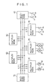
- a multipath transmission system is incorporated in a car.
- the multipath transmission system includes a plurality of multiplex nodes, for example, multiplex nodes 10 to 70 and signal transmission lines A, B and C.
- the multiplex nodes 10 to 70 are connected in parallel to the three signal transmission lines A, B and C.
- the multiplex nodes 10 to 70 transmit data signals via the signal transmission lines A, B and C.
- the multiplex node 10 is connected with a headlight 11 and a turn signal light 12
- the multiplex node 20 is connected with a door lock motor 21 and a door unlock motor 22
- the multiplex node 30 is connected with a headlight switch 31 and a turn signal switch 32
- the multiplex node 40 is connected with a door lock switch 41 and a door unlock switch 42.
- the multiplex node 10 turns on or off the headlight 11 and the turn signal light 12 in response to signals of the headlight switch 31 and the turn signal switch 32 transmitted from the multiplex node 30.
- the multiplex node 20 drives the door lock motor 21 and door unlock motor 22 in response to signals of the door lock switch 41 and door unlock switch 42 transmitted from the multiplex node 40.
- the multiplex node 50 controls an air conditioner (not shown) in the car
- the multiplex node 60 controls an operation switch (not shown) of the air conditioner
- various signals for controlling the air conditioner are transmitted between the multiplex nodes 50 and 60.
- the multiplex node 70 is connected with various indicators (not shown).
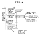
- Fig. 2 is a diagram concretely showing the multiplex node 10 of the multipath transmission system shown in Fig. 1.
- the construction of the multiplex nodes 20, 30, 50 and 60 is the same as that of the multiplex node 10, and the construction of the multiplex node 10 is explained as an example here for convenient explanation.
- the multiplex node 10 includes a communication control device 11 for effecting the communication process control, a transmission control circuit 12 for receiving a transmission signal from the communication control device 11 and transmitting the same to the signal transmission lines A, B and C, a reception control circuit 13 for supplying reception signals received from the signal transmission lines A, B and C to the communication control device 11, and a voltage detection circuit 14 for detecting a voltage of one of the signal transmission lines.
- the communication control device 11 effects the communication process control for receiving an output signal from the device connected thereto, constructing the output signal in a frame configuration for each preset data unit, and transmitting the signal formed in the frame configuration as a transmission signal to the transmission control circuit 12. Further, the communication control device 11 effects the communication process control for receiving a reception signal formed in the frame configuration from the reception control circuit 13, deriving only a signal necessary therefor from the reception signal,transmitting the signal to the device connected thereto, and transmitting an acknowledge signal (ACK signal) to the transmission control circuit 12 when the signal reception is correctly effected.
- ACK signal acknowledge signal
- the transmission control circuit 12 is connected to the multiple transmission lines A, B and C, converts a transmission signal (including the ACK signal) from the communication control device 11 and transmits the same to the multiple transmission lines A, B and C.
- the reception control circuit 13 is connected to the multiple transmission lines A, B and C, and when receiving a reception signal (including the ACK signal) from the multiple transmission lines A, B and C, it outputs the reception signal to the communication control device 11.
- the voltage detection circuit 14 is connected to one of the transmission lines, for example, the transmission line C, the communication control device 11, the transmission control circuit 12 and the reception control circuit 13, and it detects a voltage of the transmission line C and informs the communication control device 11, the transmission control circuit 12 and the reception control circuit 13 of the state of the transmission line C.
- a multiplex node 40 connected to the terminal ends of signal transmission lines A, B and C includes a communication control device 41, a transmission control circuit 42, a reception control circuit 43 and a voltage detection circuit 44 having the same function as the multiplex node 10 and further includes a terminal circuit 45 having terminal resistors connected to both ends of the transmission lines A, B and C.
- a multiplex node 70 connected to the terminal ends includes a communication control device 71, a transmission control circuit 72, a reception control circuit 73, a voltage detection circuit 74 and a terminal resistor 75 having the same function as the multiplex node 40 and further includes a voltage generation circuit 76 for applying a voltage to the signal transmission line C.
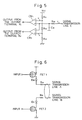
- each of the voltage detection circuits is shown in Fig. 5.
- one terminal of a voltage comparator circuit CM1 and one terminal of a voltage comparator circuit CM2 are supplied with a voltage V o of the transmission line C via a filter circuit formed of a resistor R10 and a capacitor C10.
- the other terminal of the voltage comparator circuit CM1 and the other terminal of the voltage comparator circuit CM2 are supplied with reference voltages V1 and V2 which are obtained by dividing a power source voltage Vcc by resistors R11 to R13.
- the voltage comparator circuits CM1 and CM2 check whether or not the voltage V o of the transmission line C is within the range of the reference voltages V1 and V2 by comparing the voltages applied to both of the terminals. That is, when the voltage V o is within the range of the reference voltages V1 and V2, the voltage comparator circuits CM1 and CM2 output "0" and "0” indicating the normal state to output terminals K1 and K2. When the voltage V o exceeds the range of the reference voltages V1 and V2, for example, when the transmission line B is broken on the ground, the voltage comparator circuits CM1 and CM2 output "0" and "1” indicating the abnormal state to the output terminals K1 and K2.
- the voltage comparator circuits CM1 and CM2 When the voltage V o exceeds the range of the reference voltages V1 and V2, for example, when failure occurs anywhere in the voltage detection, circuits and the transmission line C, the voltage comparator circuits CM1 and CM2 output "1" and "0" indicating the abnormal state to the output terminals K1 and K2.
- each of the transmission control circuits is shown in Fig. 6.
- the drain terminals of FET1 and FET2 are connected to filter circuits formed of diodes D10 and D11 and resistors R14 and R15.
- the FET1 is connected to a filter circuit formed of the diode D10 and the resistor R14 to the transmission line A.
- the FET2 is connected to a filter circuit formed of the diode D11 and the resistor R15 to the transmission line B. That is, when the multiplex node is set in the passive state, each FET is set in the OFF state so that no potential difference may occur between the signal transmission lines A and B and a high impedance state may occur at the output terminals.
- each FET when the multiplex node is set in the dominant state, each FET is set in the ON state, causing a current to flow into the signal transmission line A and receiving a current from the other transmission line B. Therefore, in the dominant state, a potential difference incurs between the signal transmission lines A and B and the reception circuit connected to the signal transmission lines A and B detects the potential difference. As a result, the communication control device can detect the dominant state.
- each reception control circuit is shown in Fig. 7.
- a power source voltage 1/2 Vcc is applied to the signal transmission lines A, B and C via resistors R16, R17 and R18.
- One-side ends of the signal transmission lines A, B and C are connected to the input terminals of a voltage comparator CM3 via switching elements S1 to S4 shown in the drawing.
- the ON/OFF states of the switching elements S1 to S4 are controlled by the voltage detection circuit, and the voltage detection circuit controls the ON/OFF states of the switching elements S1 to S4 in response to signals input from the output terminals K1 and K2 according to combinations shown in the following first table.
- Resistors R16 to R23 are resistors for voltage division and setting of the threshold voltage.
- the reception control circuit transmits signals in the balanced transmitting condition set by using the positive logic for the signal transmission line A and the negative logic for the signal transmission line B in the normal state in which outputs of the output terminals K1 and K2 are "0" and "0". That is, the signal reception is effected by setting the signal transmission line A in the dominant state when a voltage is high and setting the signal transmission line B in the dominant state when a voltage is low.
- the reception control circuit receives signals in the unbalanced transmitting condition set by using the signal transmission line C as a fixed potential line and the negative logic for the signal transmission line B in the abnormal state in which outputs of the output terminals K1 and K2 are "1" and "0" and receives signals in the unbalanced transmitting condition set by using the signal transmission line C as a fixed potential line and the positive logic for the signal transmission line A in the abnormal state in which outputs of the output terminals K1 and K2 are "0" and "1".
- the cost of the signal transmission line can be reduced equivalent to that of the conventional two-core shielded line.
- a resistor R E connected between the ends of the signal transmission lines A and B is divided into two portions of R E /2 by the signal transmission line C, and the signal transmission line C is connected to switching elements S5 and S6 via a resistor R24.
- the resistance of the resistor R24 is relatively smaller than that of the terminal resistor.
- the switching element S5 is constructed to be turned on when an output SK1 from the communication control device is "1" and the switching element S6 is constructed to be turned on when an output SK2 from the communication control device is "1".
- the terminal circuit 45 is also used instead of the voltage generation circuit 76 for the signal transmission line C, and when it is required to forcedly set outputs of the output terminals K1 and K2 to "1" and "0" in the multiplex node 70, for example, the switching element S5 is turned on by the control of the communication control device 71. When it is required to forcedly set outputs of the output terminals K1 and K2 to "0" and "1", the switching element S6 is turned on by the control of the communication control device 71.
- the terminal circuit 45 and the voltage generation circuit 76 which can control the voltage in the signal transmission line C are included in a system. So far as controlling of each other is concerned, output terminals SK1 and SK2 of terminal circuit 45 and that of the voltage generation circuit 76 are operated each other by synchronization, or are respectively used as main or sub.
- the outputs of the output terminals K1 and K2 of the voltage detection circuit 74 are set to the normal state of "0" and "0" and the switching elements S1 and S4 among the switching elements S1 to S4 are set shown in Fig. 7 in the ON state and the switching elements S2 and S3 are set in the OFF state.
- the communication control device 71 can check whether the signal transmission can be effected or not according to whether each multiplex node, for example, the multiplex node 30 for the multiplex node 10 or the multiplex node 40 for the multiplex node 20 can correctly transmit frames or not when the frame of the transmission signal is received (step 101).
- step 102 whether communication with all of the multiplex nodes is possible or not is checked by determining the reception of an ACK signal from all of the multiplex nodes in the same manner as described above (step 102). In this case, if it is determined that the communication is possible, the normal state in which the outputs SK1 and SK2 from the communication control device are set at "0" and "0" is maintained (step 103) and the checking operation in the step 101 is effected again.
- the output terminals SK1 and SK2 of communication control device 71 are set at the output state of "1" and "0"(step 104), therefore the output state of the output terminals K1 and K2 are set in the state of "1" and "0” and the switching elements S1, and S3 among the switching elements S1 to S4 of the reception control circuit 73 shown in Fig. 7 are set in the ON state and the switching elements S2 and S4 are set in the OFF state. Then, whether transmission with respect to the reception multiplex node is possible or not is checked in the same manner as in the step 101 (step 105).
- step 106 whether communication with all of the multiplex nodes is possible or not is checked in the same manner as in the step 102. In this case, if the communication is possible, the outputs of the output terminals SK1 and SK2 are kept at the output state of "1" and "0" (step 107) and then the determination in the step 105 is effected again.
- the switching elements S5 and S6 of the voltage generating circuit 76 are respectively forcedly turned off and on to change the output state of the output terminals K1 and K2 of voltage detecting circuit 74 to the state of "0" and "1" (step 108). And the switching elements S1 and S3 among the switching elements S1 to S4 of the reception control circuit 73 shown in Fig. 7 are set in the OFF state and the switching elements S2 and S4 are set in the ON state. Then, whether transmission with respect to the reception multiplex node is possible or not is checked in the same manner as in the step 101 (step 109).
- step 110 whether communication with all of the multiplex nodes is possible or not is checked in the same manner as in the step 102 (step 110). In this case, if the communication is possible, the outputs SK1 and SK2 from the communication control device are kept in the output state of "0" and "1" (step 111) and then the determination in the step 109 is effected again.
- step 109 If it is detected in the step 109 that the transmission is impossible, or when it is determined in the step 110 that communication with all of the multiplex nodes is impossible, it is determined that the fault is not in the transmission line and the switching elements S5 and S6 of the voltage generation circuit 76 are forcedly set in the OFF state to return the output state of the output terminals K1 and K2 to the state of "0" and "0" (step 112). Then, the operation for another fault correction routine is effected (step 113).
- the output terminals SK1 and SK2 are set to the state of "1" and "0", so that the switching elements S1 and S3 among the switching elements S1 to S4 of the reception control circuit 73 shown in Fig. 7 can be set in the ON state and the switching elements S2 and S4 can be set in the OFF state. If the transmission is possible in this state, a potential occurs between the signal transmission lines C and B in the dominant state as shown in Fig. 11. As a result, the reception control circuit 73 connected to the signal transmission lines C and B detects the potential difference and the communication control circuit 51 can detect the dominant state. In this case, the potential of the transmission line A may be freely set.
- the output terminals SK1 and SK2 are changed to the state of "0" and "1" when the transmission is impossible so that the switching elements S1 and S3 among the switching elements S1 to S4 of the reception control circuit 73 shown in Fig. 7 can be set in the OFF state and the switching elements S2 and S4 can be set in the ON state. If the transmission is possible in this state, a potential occurs between the signal transmission lines A and C in the dominant state as shown in Fig. 12. As a result, the reception control circuit 73 connected to the signal transmission lines A and C detects the potential difference and the communication control device 71 can detect the dominant state. In this case, the potential of the transmission line B may be freely set.
- the multipath transmission system of this invention even when an accident such as breakage or short-circuit occurs in the signal transmission line, a preset potential occurs between the signal transmission lines so as to permit the signal transmission between the multiplex nodes, thereby making it possible to enhance the reliability of the multiplex transmission of the whole system.
- the reception control circuit includes three voltage comparator circuits CM4 to CM6 and a select circuit SE connected to the output terminals of the voltage comparator circuits CM4 to CM6.
- a power source voltage 1/2 Vcc is applied to the transmission lines A, B and C via resistors R25, R26 and R27 in the same manner as shown in Fig. 7.
- One-side ends of the transmission lines A, B and C and the input terminals of the voltage comparator circuits CM4 to CM6 are connected as shown in the drawing.
- the select circuit SE receives output signals (potential difference) from the voltage comparator circuits CM4 to CM6.
- a plurality of switching elements shown in Fig. 7 are not necessary, thus making it possible to reduce the number of parts used.
Landscapes
- Engineering & Computer Science (AREA)
- Computer Networks & Wireless Communication (AREA)
- Signal Processing (AREA)
- Power Engineering (AREA)
- Small-Scale Networks (AREA)
- Dc Digital Transmission (AREA)
Applications Claiming Priority (2)
| Application Number | Priority Date | Filing Date | Title |
|---|---|---|---|
| JP113751/90 | 1990-04-27 | ||
| JP2113751A JP2851124B2 (ja) | 1990-04-27 | 1990-04-27 | 多重伝送方式 |
Publications (3)
| Publication Number | Publication Date |
|---|---|
| EP0454505A2 true EP0454505A2 (de) | 1991-10-30 |
| EP0454505A3 EP0454505A3 (en) | 1993-02-03 |
| EP0454505B1 EP0454505B1 (de) | 1999-04-07 |
Family
ID=14620203
Family Applications (1)
| Application Number | Title | Priority Date | Filing Date |
|---|---|---|---|
| EP91303879A Expired - Lifetime EP0454505B1 (de) | 1990-04-27 | 1991-04-29 | Mehrwegübertragungssystem |
Country Status (6)
| Country | Link |
|---|---|
| US (1) | US5321689A (de) |
| EP (1) | EP0454505B1 (de) |
| JP (1) | JP2851124B2 (de) |
| KR (1) | KR910019368A (de) |
| CA (1) | CA2041309A1 (de) |
| DE (1) | DE69131082T2 (de) |
Cited By (2)
| Publication number | Priority date | Publication date | Assignee | Title |
|---|---|---|---|---|
| EP0569600A4 (de) * | 1991-12-02 | 1995-01-18 | Furukawa Electric Co Ltd | Verfahren zur beseitigung einer gestörten übertragungsleitung. |
| EP0785649A3 (de) * | 1995-11-27 | 2001-06-06 | Italtel s.p.a. | Verfahren und Vorrichtung zur Korrektur von Übertragungsfehlern und Erkennung von Fehlern während der Übertragung von Daten über ein Datenübertragungsmedium |
Families Citing this family (22)
| Publication number | Priority date | Publication date | Assignee | Title |
|---|---|---|---|---|
| DE69132259T2 (de) * | 1990-12-04 | 2000-10-26 | The Furukawa Electric Co., Ltd. | Vorrichtung zur spannungseinstellung in einem multiplexübertragungssystem |
| EP0613428B1 (de) * | 1991-11-26 | 1995-06-14 | Siemens Aktiengesellschaft | Bussystem |
| DE4229175A1 (de) * | 1992-09-02 | 1994-03-03 | Bosch Gmbh Robert | Netzwerkschnittstelle |
| SE9700633L (sv) * | 1997-02-21 | 1998-03-16 | Mecel Ab | Metod och arrangemang för kombinerad data och kraftöverföring på kommunikationsbussar |
| EP1001257B1 (de) * | 1998-05-29 | 2005-12-21 | Mitsubishi Denki Kabushiki Kaisha | System und verfahren zur überwachung von fahrzeugen |
| US8194536B2 (en) * | 2001-08-31 | 2012-06-05 | Continental Automotive Systems, Inc. | Vehicle active network with fault tolerant devices |
| US20030043824A1 (en) * | 2001-08-31 | 2003-03-06 | Remboski Donald J. | Vehicle active network and device |
| US20030043793A1 (en) * | 2001-08-31 | 2003-03-06 | Juergen Reinold | Vehicle active network |
| US6766482B1 (en) | 2001-10-31 | 2004-07-20 | Extreme Networks | Ethernet automatic protection switching |
| DE102004042380A1 (de) * | 2004-09-02 | 2006-03-09 | Robert Bosch Gmbh | Datenbus-Interface für ein Steuergerät und Steuergerät mit einem Datenbus-Interface |
| US7593429B2 (en) * | 2004-10-14 | 2009-09-22 | Temic Automotive Of North America, Inc. | System and method for time synchronizing nodes in an automotive network using input capture |
| US7623552B2 (en) * | 2004-10-14 | 2009-11-24 | Temic Automotive Of North America, Inc. | System and method for time synchronizing nodes in an automotive network using input capture |
| US20060083172A1 (en) * | 2004-10-14 | 2006-04-20 | Jordan Patrick D | System and method for evaluating the performance of an automotive switch fabric network |
| US7593344B2 (en) * | 2004-10-14 | 2009-09-22 | Temic Automotive Of North America, Inc. | System and method for reprogramming nodes in an automotive switch fabric network |
| US7599377B2 (en) * | 2004-10-15 | 2009-10-06 | Temic Automotive Of North America, Inc. | System and method for tunneling standard bus protocol messages through an automotive switch fabric network |
| US7613190B2 (en) * | 2004-10-18 | 2009-11-03 | Temic Automotive Of North America, Inc. | System and method for streaming sequential data through an automotive switch fabric |
| JP4952212B2 (ja) | 2006-11-22 | 2012-06-13 | 株式会社デンソー | 通信妨害防止装置、通信システムのノード、通信システム、車両用故障診断装置、及び車載装置 |
| US20090240853A1 (en) * | 2008-03-21 | 2009-09-24 | Rochester Institute Of Technology | Method and apparatus for configuring a bus network in an asset management system |
| US20120143438A1 (en) * | 2010-12-01 | 2012-06-07 | Nissan North America, Inc. | Fiber optic vehicle communication system |
| JP2013150148A (ja) * | 2012-01-19 | 2013-08-01 | Denso Corp | 通信システム及び通信線切り替え制御方法 |
| US9787494B2 (en) * | 2013-10-25 | 2017-10-10 | Fts Computertechnik Gmbh | Method for transmitting messages in a computer network, and computer network |
| US11264832B2 (en) * | 2016-10-19 | 2022-03-01 | Sony Semiconductor Solutions Corporation | Signal processing device, signal processing method, and program |
Family Cites Families (7)
| Publication number | Priority date | Publication date | Assignee | Title |
|---|---|---|---|---|
| JPS5634256A (en) * | 1979-08-29 | 1981-04-06 | Fuji Electric Co Ltd | Data transmission system |
| US4463352A (en) * | 1982-07-06 | 1984-07-31 | Honeywell Inc. | Fault tolerant, self-powered data reporting system |
| NL8500571A (nl) * | 1985-03-01 | 1986-10-01 | Hollandse Signaalapparaten Bv | Locaal data-communicatienetwerk volgens het multiple-bus-systeem. |
| US4847832A (en) * | 1986-10-21 | 1989-07-11 | Amp Incorporated | Time multiplexed data transmission system |
| US4677308A (en) * | 1986-12-22 | 1987-06-30 | Chrysler Motors Corporation | Switch status monitoring system, single wire bus, smart sensor arrangement therefor |
| FR2627036B1 (fr) * | 1988-02-10 | 1990-07-27 | Peugeot | Interface de raccordement d'une partie de reception d'informations d'une station dans un systeme de transmission d'informations en differentiel, par deux fils de transmission, notamment dans un vehicule automobile |
| US4964120A (en) * | 1989-09-08 | 1990-10-16 | Honeywell Inc. | Method of detecting a cable fault and switching to a redundant cable in a universal local area network |
-
1990
- 1990-04-27 JP JP2113751A patent/JP2851124B2/ja not_active Expired - Lifetime
-
1991
- 1991-04-26 CA CA002041309A patent/CA2041309A1/en not_active Abandoned
- 1991-04-26 KR KR1019910006771A patent/KR910019368A/ko not_active Withdrawn
- 1991-04-29 DE DE69131082T patent/DE69131082T2/de not_active Expired - Fee Related
- 1991-04-29 EP EP91303879A patent/EP0454505B1/de not_active Expired - Lifetime
-
1993
- 1993-03-01 US US08/024,815 patent/US5321689A/en not_active Expired - Fee Related
Cited By (2)
| Publication number | Priority date | Publication date | Assignee | Title |
|---|---|---|---|---|
| EP0569600A4 (de) * | 1991-12-02 | 1995-01-18 | Furukawa Electric Co Ltd | Verfahren zur beseitigung einer gestörten übertragungsleitung. |
| EP0785649A3 (de) * | 1995-11-27 | 2001-06-06 | Italtel s.p.a. | Verfahren und Vorrichtung zur Korrektur von Übertragungsfehlern und Erkennung von Fehlern während der Übertragung von Daten über ein Datenübertragungsmedium |
Also Published As
| Publication number | Publication date |
|---|---|
| DE69131082T2 (de) | 2000-01-05 |
| EP0454505A3 (en) | 1993-02-03 |
| JP2851124B2 (ja) | 1999-01-27 |
| DE69131082D1 (de) | 1999-05-12 |
| JPH0410828A (ja) | 1992-01-16 |
| EP0454505B1 (de) | 1999-04-07 |
| KR910019368A (ko) | 1991-11-30 |
| US5321689A (en) | 1994-06-14 |
| CA2041309A1 (en) | 1991-10-28 |
Similar Documents
| Publication | Publication Date | Title |
|---|---|---|
| EP0454505A2 (de) | Mehrwegübertragungssystem | |
| KR100192073B1 (ko) | 디지탈 이선 버스 자료 통신시스템 고장-허용 출력스테이지 | |
| US5696777A (en) | Device for the serial transmission of data between at least two terminals | |
| US5572658A (en) | Network interface | |
| KR20000005107A (ko) | 데이터 전송을 위한 버스 시스템 | |
| EP0383291A1 (de) | Übertragungsfehler-Diagnosevorrichtung | |
| US5550804A (en) | Data bus system | |
| JP3828035B2 (ja) | 空気調和機の運転制御装置及びマルチ式空気調和機の運転制御装置 | |
| US4642807A (en) | Fault tolerant receiver | |
| KR960009471B1 (ko) | 다중전송방법 | |
| JPH03254246A (ja) | Lan用伝送システム | |
| JP2726300B2 (ja) | 故障診断装置 | |
| KR200195844Y1 (ko) | 점검장치와 전자제어장치간 통신 장치 | |
| JPH04344738A (ja) | 多重伝送方式 | |
| JP3221259B2 (ja) | バス型二重化伝送装置 | |
| KR200178397Y1 (ko) | 점검장치와 전자제어장치간 통신장치 | |
| JPH023342B2 (de) | ||
| JP2721457B2 (ja) | 信号切替回路 | |
| JP2851085B2 (ja) | 端末電源断検出方法 | |
| KR810002109B1 (ko) | 통신 접속부 회로 | |
| JPH05260063A (ja) | ネットワーク中継装置およびネットワークシステムの監視方法 | |
| EP0569600A1 (de) | Verfahren zur beseitigung einer gestörten übertragungsleitung | |
| JP3082508B2 (ja) | 駆動回路の異常検出回路 | |
| EP0978970A2 (de) | Fehlertoleranter, differentieller Empfänger | |
| JPH0120828B2 (de) |
Legal Events
| Date | Code | Title | Description |
|---|---|---|---|
| PUAI | Public reference made under article 153(3) epc to a published international application that has entered the european phase |
Free format text: ORIGINAL CODE: 0009012 |
|
| AK | Designated contracting states |
Kind code of ref document: A2 Designated state(s): DE FR GB IT NL SE |
|
| PUAL | Search report despatched |
Free format text: ORIGINAL CODE: 0009013 |
|
| AK | Designated contracting states |
Kind code of ref document: A3 Designated state(s): DE FR GB IT NL SE |
|
| 17P | Request for examination filed |
Effective date: 19930727 |
|
| GRAG | Despatch of communication of intention to grant |
Free format text: ORIGINAL CODE: EPIDOS AGRA |
|
| 17Q | First examination report despatched |
Effective date: 19980504 |
|
| GRAG | Despatch of communication of intention to grant |
Free format text: ORIGINAL CODE: EPIDOS AGRA |
|
| GRAH | Despatch of communication of intention to grant a patent |
Free format text: ORIGINAL CODE: EPIDOS IGRA |
|
| GRAH | Despatch of communication of intention to grant a patent |
Free format text: ORIGINAL CODE: EPIDOS IGRA |
|
| GRAA | (expected) grant |
Free format text: ORIGINAL CODE: 0009210 |
|
| AK | Designated contracting states |
Kind code of ref document: B1 Designated state(s): DE FR GB IT NL SE |
|
| PG25 | Lapsed in a contracting state [announced via postgrant information from national office to epo] |
Ref country code: IT Free format text: LAPSE BECAUSE OF FAILURE TO SUBMIT A TRANSLATION OF THE DESCRIPTION OR TO PAY THE FEE WITHIN THE PRE;WARNING: LAPSES OF ITALIAN PATENTS WITH EFFECTIVE DATE BEFORE 2007 MAY HAVE OCCURRED AT ANY TIME BEFORE 2007. THE CORRECT EFFECTIVE DATE MAY BE DIFFERENT FROM THE ONE RECORDED.SCRIBED TIME-LIMIT Effective date: 19990407 Ref country code: SE Free format text: THE PATENT HAS BEEN ANNULLED BY A DECISION OF A NATIONAL AUTHORITY Effective date: 19990407 Ref country code: NL Free format text: LAPSE BECAUSE OF FAILURE TO SUBMIT A TRANSLATION OF THE DESCRIPTION OR TO PAY THE FEE WITHIN THE PRESCRIBED TIME-LIMIT Effective date: 19990407 |
|
| REF | Corresponds to: |
Ref document number: 69131082 Country of ref document: DE Date of ref document: 19990512 |
|
| ET | Fr: translation filed | ||
| PG25 | Lapsed in a contracting state [announced via postgrant information from national office to epo] |
Ref country code: GB Free format text: LAPSE BECAUSE OF NON-PAYMENT OF DUE FEES Effective date: 19990707 |
|
| NLV1 | Nl: lapsed or annulled due to failure to fulfill the requirements of art. 29p and 29m of the patents act | ||
| PLBE | No opposition filed within time limit |
Free format text: ORIGINAL CODE: 0009261 |
|
| STAA | Information on the status of an ep patent application or granted ep patent |
Free format text: STATUS: NO OPPOSITION FILED WITHIN TIME LIMIT |
|
| GBPC | Gb: european patent ceased through non-payment of renewal fee |
Effective date: 19990707 |
|
| 26N | No opposition filed | ||
| PGFP | Annual fee paid to national office [announced via postgrant information from national office to epo] |
Ref country code: FR Payment date: 20000411 Year of fee payment: 10 |
|
| PG25 | Lapsed in a contracting state [announced via postgrant information from national office to epo] |
Ref country code: FR Free format text: THE PATENT HAS BEEN ANNULLED BY A DECISION OF A NATIONAL AUTHORITY Effective date: 20010430 |
|
| REG | Reference to a national code |
Ref country code: FR Ref legal event code: ST |
|
| PGFP | Annual fee paid to national office [announced via postgrant information from national office to epo] |
Ref country code: DE Payment date: 20020508 Year of fee payment: 12 |
|
| PG25 | Lapsed in a contracting state [announced via postgrant information from national office to epo] |
Ref country code: DE Free format text: LAPSE BECAUSE OF NON-PAYMENT OF DUE FEES Effective date: 20031101 |