EP0454579A2 - Non-volatile semiconductor memory device having EEPROM cell, dummy cell and sense circuit for increasing reliability and enabling one-bit operation - Google Patents
Non-volatile semiconductor memory device having EEPROM cell, dummy cell and sense circuit for increasing reliability and enabling one-bit operation Download PDFInfo
- Publication number
- EP0454579A2 EP0454579A2 EP91401092A EP91401092A EP0454579A2 EP 0454579 A2 EP0454579 A2 EP 0454579A2 EP 91401092 A EP91401092 A EP 91401092A EP 91401092 A EP91401092 A EP 91401092A EP 0454579 A2 EP0454579 A2 EP 0454579A2
- Authority
- EP
- European Patent Office
- Prior art keywords
- memory device
- semiconductor memory
- volatile semiconductor
- cell
- circuit
- Prior art date
- Legal status (The legal status is an assumption and is not a legal conclusion. Google has not performed a legal analysis and makes no representation as to the accuracy of the status listed.)
- Granted
Links
Images







Classifications
-
- G—PHYSICS
- G11—INFORMATION STORAGE
- G11C—STATIC STORES
- G11C16/00—Erasable programmable read-only memories
-
- G—PHYSICS
- G11—INFORMATION STORAGE
- G11C—STATIC STORES
- G11C16/00—Erasable programmable read-only memories
- G11C16/02—Erasable programmable read-only memories electrically programmable
- G11C16/06—Auxiliary circuits, e.g. for writing into memory
- G11C16/26—Sensing or reading circuits; Data output circuits
- G11C16/28—Sensing or reading circuits; Data output circuits using differential sensing or reference cells, e.g. dummy cells
-
- G—PHYSICS
- G11—INFORMATION STORAGE
- G11C—STATIC STORES
- G11C7/00—Arrangements for writing information into, or reading information out from, a digital store
Definitions
- the present invention relates to a non-volatile semiconductor memory device, more particularly, to a non-volatile semiconductor memory device using an electrically erasable programmable read only memory (EEPROM) cell, a dummy cell, and a sense circuit.
- EEPROM electrically erasable programmable read only memory
- an EEPROM which can be reprogrammed by electrically erasing the contents previously programmed therein, have come to be preferred over EPROMs which are erased by being irradiates with ultraviolet light.
- an EEPROM can be used for on-vehicle equipment (e.g., for setting control parameters or codes suitable for an application environment), a measuring apparatus, a camera, a telephone set (e.g., for storing telephone numbers), a telemetering system, a fuzzy control apparatus, and the like.
- EEPROM non-volatile semiconductor memory device
- a non-volatile semiconductor memory device comprises an EEPROM cell, transfer gates for selecting the EEPROM cell in response to a select signal applied to a word select line WSL, a write/erase circuit, and a current sense type sense circuit.
- the EEPROM cell includes a control electrode, a floating gate, a drain, and a source.
- non-volatile semiconductor memory devices EEPROMs
- a plurality of bits of a specific group for example, each column unit, or each word unit
- an erase cycle and a write cycle are carried out individually, so that the required time for a rewriting operation becomes long.
- the cell to be written into is previously erased and is then rewritten the cell itself is deteriorated.
- the required time for a rewriting operation becomes long and cells are deteriorated in a short time, because an erase operation and a write operation are individually carried out.
- a plurality of single polysilicon EEPROM cells are developed and provided.
- such single polysilicon EEPROM cells are disclosed in Japanese Unexamined Patent Publication (Kokai) No. 59-155968 (corresponding to U.S. Patent No. 4,642,673), Japanese Unexamined Patent Publication (Kokai) No. 63-156361 (corresponding to U.S. Patent No. 4,807,003), Japanese Unexamined Patent Publication (Kokai) No. 63-166274, and the like.
- These single polysilicon EEPROM cells can be used in a non-volatile semiconductor memory device according to the present invention.
- a non-volatile semiconductor memory device comprising: a first and second signal lines; a memory cell, operatively connected to the first and second signal lines, for storing data; a dummy cell, operatively connected to the first and second signal lines; and a sense circuit, for amplifying the difference between a potential of the first signal line and a potential of the second signal line; wherein, when a first current flowing through the memory cell from the first signal line, in response to data stored in the memory cell, is larger than a second current flowing through the dummy cell from the second signal line at a read-out operation, the second current is decreased; and when the first current is smaller than the second current at the read-out operation, the second current is increased.
- a micro-controller formed in a single semiconductor body comprising: a central processing unit core; an input/output port, connected to the central processing unit core, for inputting and outputting data and signals; a memory portion, connected to the central processing unit core, for writing, erasing, and reading out data in accordance with the control of the central processing unit core.
- the memory portion may comprise: a first and second signal lines; a memory cell, operatively connected to the first and second signal lines, for storing data; a dummy cell, operatively connected to the first and second signal lines; and a sense circuit, for amplifying the difference between a potential of the first signal line and a potential of the second signal line; wherein, when a first current flowing through the memory cell from the first signal line, in response to data stored in the memory cell, is larger than a second current flowing through the dummy cell from the second signal line at a read-out operation, the second current is decreased; and when the first current is smaller than the second current at the read-out operation, the second current is increased.
- the non-volatile semiconductor memory device may further comprise: a first and second transfer gates, provided between the memory cell and the first and second signal lines; a word select line, applied with a word select signal for controlling the first and second transfer gates; a third and fourth transfer gates, provided between the dummy cell and the first and second signal lines; and a dummy word select line, applied with a dummy word select signal for controlling the third and fourth transfer gates.
- a gate of the dummy cell may be connected to the first signal line through the third transfer gate, a drain thereof may be connected to the second signal line through the fourth transfer gate, and a source thereof may be connected to the ground through a fifth transfer gates controlled by a read control signal.
- the non-volatile semiconductor memory device may further comprise a write stabilizing circuit, connected to the first and second signal lines, for improving reliability at a write operation, and an output line of the write stabilizing circuit is connected to the memory cell.
- the output line of the write stabilizing circuit may be connected to the ground through a sixth transfer gate controlled by a read control signal.
- the non-volatile semiconductor memory device may further comprise a first high-voltage switching circuit connected to the first signal line and a second high-voltage switching circuit connected to the second signal line, for boosting and applying a write/erase power supply voltage between the first and second signal lines by using a pumping clock signal.
- the memory cell may comprise: a cell transistor, including a floating gate, a drain connected to the first signal line through the first transfer gate, and a source connected to an output line of a write stabilizing circuit, for storing data by injecting electrons into the floating gate; and a control gate, including a control electrode connected to the second signal line through the second transfer gate, and a floating electrode connected to the floating gate of the cell transistor.
- the cell transistor and the dummy cell may be formed at the same size.
- a gate length and a gate width of the dummy cell may be formed the same as a gate length and a gate width of the cell transistor.
- a gate length of the dummy cell may be determined in accordance with the characteristics of the cell transistor.
- the cell transistor and the dummy cell may be formed in the same processes of producing the non-volatile semiconductor memory device.
- the memory cell may include a single polycrystal line silicon layer of a large occupied area, and the first and second signal lines may be wired above the area occupied by the memory cell.
- the memory cell may be an EEPROM cell.
- the sense circuit may be a differential type sense amplifier.
- the sense circuit may be connected to the first and second signal lines through a seventh and eighth transfer gates with a bias voltage applied thereto.
- the sense circuit may be used to write specific data into the the memory cell.
- the first and second signal lines and an output line of a write stabilizing circuit may be plurally provided, the memory cell may be plurally provided in parallel to each group of the first and second signal lines and the output lines of the write stabilizing circuit through a select circuit, and one of the plurality of memory cells may be selected in response to select signals applied to the select circuit.
- the non-volatile semiconductor memory device may further comprise: a high voltage generation portion for applying a high voltage to the memory cell; an address latch circuit for latching input and output addresses; and a data latch circuit for latching input and output data.
- the non-volatile semiconductor memory device may be formed in a single semiconductor body and the non-volatile semiconductor memory device may further comprise: a high voltage generation circuit, connected to the sense circuit, for applying a high voltage to the memory cell; an address buffer, connected to a column decoder, a row decoder, and a dummy word decoder, for inputting and outputting addresses; a data input/output portion connected to the sense circuit, for inputting and outputting data; and a control signal buffer for receiving control signals; and a control logic circuit, connected to the control signal buffer, for controlling the state of the non-volatile semiconductor memory device.
- the non-volatile semiconductor memory device may further comprise: a threshold voltage measuring column including a test dummy cell and a test sense circuit, for estimating a threshold voltage of the memory cell by measuring the test dummy cell, a threshold voltage measuring terminal, connected to the threshold voltage measuring column, for applying various voltages, and a threshold voltage measuring input/output portion, connected to the test sense circuit, for inputting or detecting data to measure the threshold voltage of the memory cell when applying various voltages to the threshold voltage measuring terminal.
- a threshold voltage measuring column including a test dummy cell and a test sense circuit, for estimating a threshold voltage of the memory cell by measuring the test dummy cell
- a threshold voltage measuring terminal connected to the threshold voltage measuring column, for applying various voltages
- a threshold voltage measuring input/output portion connected to the test sense circuit, for inputting or detecting data to measure the threshold voltage of the memory cell when applying various voltages to the threshold voltage measuring terminal.
- FIG. 1 is a circuit diagram indicating an example of a non-volatile semiconductor memory device (EEPROM) according to the prior art.
- the EEPROM can be reprogrammed by electrically erasing the contents previously programmed in the EEPROM.
- a non-volatile semiconductor memory device comprises an EEPROM cell 801, transfer gates 831, 832 for selecting the EEPROM cell 801 in response to a select signal applied to a word select line WSL, a read bias generation circuit 800 for generating a bias voltage used in a read out operation, a write/erase circuit 802, and a current sense type sense circuit 805. Further, the non-volatile semiconductor memory device comprises: gate transistors 820 and 804, which are controlled by a read signal R and a column select signal and are provided between the cell 801 and the sense circuit 805; and transistors 851, 852 and an inverter 853 for erasing the contents written in a specific numbers of EEPROM cells 801 in response to an erase signal.
- a reference 801a denotes a control electrode
- 801b denotes a floating gate
- 801c denotes a drain
- 801d denotes a source.
- the non-volatile semiconductor memory device shown in Fig. 1 uses the current sense type sense circuit 805 without using a dummy cell, and write/erase/read-out operations are carried out thereby.
- a plurality of bits of a specific group for example, each column unit, or each word unit
- a latch operation must be carried out when writing data to the EEPROM cell 801, however, write/erase/read-out operations are carried out by using a current sense type sense circuit 805.
- a bias generation circuit 800 which is used to generate a bias voltage for applying to a gate (control electrode 801a) of an EEPROM cell 801 at the read-out operation, must be provided. Therefore, a time for setting the bias voltage output from the bias generation circuit 800 becomes an obstruction to high speed access.
- an erase cycle (about 10 msec.) and a write cycle (about 10 msec.) are individually carried out, and thus the required time for a rewriting operation becomes long, i.e., determined at about 20 msec.
- the cell to be written is previously erased and it is rewritten thereafter, and thus the cell deteriorates at double the speed in worst case.
- the required time for a rewriting operation becomes long and cells are deteriorated in a short time, because an erase operation and a write operation are individually carried out.
- a threshold voltage Vth of an EEPROM cell may by fluctuated by the processes of producing the EEPROM cell on a semiconductor substrate.
- Figure 2 is a diagram indicating a principle of a non-volatile semiconductor memory device according to the present invention.
- the non-volatile semiconductor memory device of the present invention comprises a first and second control lines 21, 22 (or a drain column line DCL, and a control column line CCL), an EEPROM cell 1, a dummy cell 101, and a sense circuit 5.
- the first and second control lines 21, 22 are applied with an actuating signal and an inverted signal thereof to control write, erase and read-out operations.
- the EEPROM cell 1 is connected to the first and second control lines 21, 22 through a first and second transfer gates 31, 32, and these first and second transfer gates 31, 32 are controlled by a word select signal applied to a word select line 4.
- the dummy cell 101 is connected to the first and second control lines 21, 22 through a third and fourth transfer gates 131, 132, and these third and fourth transfer gates 131, 132 are controlled by a dummy word select signal applied to a dummy word select line 104.
- the sense circuit 5 is connected to the first and second control lines 21, 22 to read out the content written in the EEPROM cell 1 by the difference between a current (Ir) flowing through the EEPROM cell 1 from the first control line 21 and a current (Id) flowing through the dummy cell 101 from the second control line 22. Note, the sense circuit is also used to write data into the EEPROM cell 1.
- non-volatile semiconductor memory device having the above configuration, write/erase/read-out operations of data for each one bit can be carried out in one operation (operation cycle). Therefore, in the non-volatile semiconductor memory device of the present invention, each required one bit can be written or erased in one operation, individually, the same as in a general DRAM, so that deterioration of a cell transistor can be decreased.
- an EEPROM cell transistor (11) and a dummy cell transistor (or dummy cell 101) are formed in the same processes of producing the non-volatile semiconductor memory device, so that threshold voltages of the EEPROM cell transistor and the dummy cell transistor are changed the same as when these threshold voltages are fluctuated by the wafer processes deviation of the non-volatile semiconductor memory device.
- Figure 3 is a diagram indicating a overall configuration of an example of a non-volatile semiconductor memory device applying the present invention, concretely, Fig. 3 indicates a system configuration for writing an EEPROM cell.
- the system of the non-volatile semiconductor memory device comprises: a memory portion 406 including an EEPROM cell, a decoder, a driver and a sense amplifier; a high voltage generation portion 400 for applying a high voltage (for example, about 12 ⁇ 23 volts sufficiently higher than the normal power supply voltage) to the memory portion 406; a write timer 407; an address latch circuit 408; a data latch circuit 409; a control signal generation circuit 410; and a write data signal generation circuit 600.
- a memory portion 406 including an EEPROM cell, a decoder, a driver and a sense amplifier
- a high voltage generation portion 400 for applying a high voltage (for example, about 12 ⁇ 23 volts sufficiently higher than the normal power supply voltage) to the memory portion 406
- the high voltage generation portion 400 comprises: a voltage doubler rectifier circuit 401 for doubling an input power supply voltage Vcc; a booster circuit 402 for boosting an output of the voltage doubler rectifier circuit 401; a constant-voltage circuit 403 for stabilizing an output of the booster circuit 402; a waveform shaping circuit 404 for waveform-shaping of an output of the constant-voltage circuit 403 in order to prevent a deterioration of a tunnel oxide film of an EEPROM cell; and a power-off/voltage-drop detection circuit 405.
- the waveform shaping circuit 404 is used to waveform-shape the output of the constant-voltage circuit 403, and the write timer 407 is used to stop the high voltage after a predetermined time by applying the output signal of the write timer 407 to the high voltage generation portion 400. Further, the high voltage is applied to the memory portion 406, and data applied to the data latch circuit 409 are written to the addresses of the memory portion 406 corresponding to address signals applied to the address latch circuit 408.
- the power-off/voltage-drop detection circuit 405 is used to detect a power failure (for example, a cut off of a power supply and a drop of a voltage) during a write operation, and is used to output the result whether the write operation is exactly carried out or not.
- non-volatile semiconductor memory device of the present invention particularly relates to the configuration of the memory portion 406.
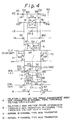
- FIG. 4 is a circuit diagram indicating an embodiment of a non-volatile semiconductor memory device according to the present invention.
- an EEPROM cell 1 is connected to a drain column line DCL (21) and a control column line CCL (22) through transfer gates 31 and 32.
- gate terminals of the MOS transistors utilized as transfer gates 31 and 32 are applied with a word select signal by a word select line 4.
- the drain column line DCL is connected to a gate of a dummy cell transistor 101 through a gate transistor 131, and the control column line CCL is connected to a drain of the dummy cell transistor 101 through a transistor 132.
- a source of the dummy cell transistor 101 is connected to the ground through a transistor 122 which is controlled by a read-out control signal R.
- the transistors 131 and 132 are controlled by a dummy word select signal which is applied to a dummy word select line DWL.
- pump circuits (high-voltage switching circuits) 71 and 72 which are used to apply a high voltage (for example, about 7 ⁇ 30 volts) between the drain column line DCL and the control column line CCL when write and erase operations are carried out, are provided to the drain column line DCL or the control column line CCL, respectively.
- these pump circuits 71 and 72 are used to transfer a write/erase power supply voltage Vpp in response to the latched data by a pumping clock signal CLK (PHIPUMP).
- a write stabilizing circuit 6 is provided between the drain column line DCL and the control column line CCL.
- This write stabilizing circuit 6 is constituted by transistors 61 ⁇ 64, and gates of the transistors 61, 64 and 62, 63 are connected to write data lines (WD, WD) each applying write data WD and WD .
- a connection portion between the transistors 63 and 64 is connected to a source column line SCL which is connected to the EEPROM cell 1. Note, this source column line SCL is connected to the ground through a transistor 121 which is controlled by the dummy word select line DWL.
- a sense circuit (differential type sense amplifier) 5 is connected to the drain column line DCL and the control column line CCL at nodes N1 and N2 through transistors 161 and 162 the gates of which have a bias voltage V B applied thereto.
- a power supply voltage Vcc is applied to the sense circuit 5, and an ground potential is applied to the sense circuit 5 through a transistor 110 which is controlled by a latch enable signal LE.
- read out data RD and RD which are output from inverters 151 and 152, are controlled by the latch enable signal LE.
- the sense circuit 5 reads out the content written in the EEPROM cell 1 by the difference between a current flowing in the control column line CCL through the dummy cell (dummy cell transistor) 101 and a current flowing in the drain column line DCL through the EEPROM cell 1.
- the levels of the node N1 and the drain column line DCL are inverted levels of the node N2 and the control column line CCL.
- the EEPROM cell 1 comprises a cell transistor 11 and a control gate 12.
- the cell transistor 11 includes a single polycrystal silicon layer (floating gate), a drain 111 of the cell transistor 11 is connected to the drain column line DCL through a transfer gate 31, and a source 113 thereof is directly connected to the source column line SCL. Further, a gate (floating gate) 112 of the cell transistor 11 is connected to an electrode (floating electrode) 12b opposite to a control electrode 12a of the control gate 12.
- the control electrode 12a is constituted by a diffusion region formed close to a surface of a semiconductor substrate.
- the cell transistor 11 of the EEPROM cell 1 and the dummy cell (dummy cell transistor) 101 can be formed at the same size. Namely, a gate length (Ld) and a gate width (Wd) of the dummy cell 101 are formed the same as a transistor length (or a gate length Lr) and a transistor width (or a gate width Wr) of the cell transistor 11.
- both currents (Ide, Idw) of an erased and written states flowing through the dummy cell 101 and the control column line CCL are determined within a current (Ire) of an erased state and a current (Irw) of a written state flowing through the cell transistor 11 and the drain column line DCL (with reference to Fig. 8).
- Figure 5 is a diagram indicating an example of programming-inhibiting characteristics of the EEPROM cell.
- write characteristics of an EEPROM cell (1) are decreased in accordance with increasing the number of write/erase operations (rewriting number). Namely, when the rewriting number becomes large, or the rewriting number is increased to about 106 times (over 104 times), the threshold difference between a written cell and an erased cell (cell transistor 11) becomes small. Note, this phenomenon (programming-inhibiting characteristics) is usually called Window Closing and is shown in Fig. 5.
- broken lines indicate another programming-inhibiting characteristics when a potential difference in a program cycle is larger than the programming-inhibiting characteristics indicated by solid lines.
- Figures 6A and 6B are circuit diagrams indicating the EEPROM cell and the dummy cell of the non-volatile semiconductor memory device shown in Fig. 4, and Figs. 7A to 7D are diagrams indicating configurations of the EEPROM cell and the dummy cell of the non-volatile semiconductor memory device shown in Fig. 4.
- Fig. 6A mainly indicate an EEPROM cell 1 including a cell transistor 11 and a control gate 12
- Fig. 6B mainly indicate a dummy cell 101.
- Fig. 7A is a plan view indicating the EEPROM cell 1
- Fig. 7B is a sectional view cut along a A-A line shown in Fig. 7A.
- Fig. 7A is a plan view indicating the EEPROM cell 1
- Fig. 7B is a sectional view cut along a A-A line shown in Fig. 7A.
- Fig. 7A is a plan view indicating the EEPROM cell 1
- FIG. 7C is a plan view indicating the dummy cell 101
- Fig. 7D is a sectional view cut along a B-B line shown in Fig. 7C.
- references 701 to 707 denote via holes passing through a layer, or contact holes connecting wirings (DCL, CCL) to a substrate, a diffusion region, or another wiring.
- the cell transistor 11 of the EEPROM cell 1 is preferably formed the same size as the dummy cell (dummy cell transistor) 101, namely, a gate length (Lr) and a gate width (Wr) of the cell transistor 11 can be formed the same as a gate length (Ld) and a gate width (Wd) of the dummy cell transistor 101 (with reference to Figs. 7A to 7D).
- a trans-conductance Gmc of the cell transistor 11 and a trans-conductance Gmd of the dummy cell transistor 101 can be specified as the same value.
- a threshold voltage V FG of the cell transistor 1 corresponds to a threshold voltage V G of the dummy cell transistor 101 detected from the sense circuit 5, and thus the following equation (1) is valid in a critical condition (V FG > V FGcrit : written state; V FG ⁇ V FGcrit : erased state).
- a charge Q corresponds to a threshold voltageshift.
- a threshold voltage Vtci of the cell transistor 11 which is defined at the floating gate 112 of the cell transistor 11, to be equal to the threshold voltage of the dummy cell transistor 101
- Vtci is specified as 0.2 volts
- Vcc L is specified as 1.2 volts
- the sense current Is is to be 10 ⁇ A
- the written charge required to cause the critical condition is obtained as 26.3 x 10 ⁇ 15 Q from the above equations.
- a reference V x (-0.49 volts) indicates the threshold voltage of the sense circuit 5.
- the EEPROM cell transistor 11 and the dummy cell transistor 101 are formed in the same wafer processes to produce the non-volatile semiconductor memory device, so that threshold voltages of the EEPROM cell transistor 11 and the dummy cell transistor 101 are changed as the same when these threshold voltages are fluctuated by deviating the wafer processing conditions from the standard.
- the cell transistor 11 and the dummy cell transistor 101 are formed at the same size, but in the present invention, the sizes of the cell transistor 11 and the dummy cell transistor 101 can be different therebetween.
- the gate length (Ld) and the gate width (Wd) of the dummy cell transistor 101 can be of different sizes from the gate length (Lr) and the gate width (Wr) of the cell transistor 11, in accordance with characteristics of the cell transistor 11 and the dummy cell transistor 101, especially, the gate length (Ld) the dummy cell transistor 101 can be determined in accordance with characteristics of the cell transistor 11.
- Figure 8 is a waveform diagram for explaining a read out operation in the non-volatile semiconductor memory device shown in Fig. 4.
- a read-out operation will be explained.
- a read-out control signal R when a read-out control signal R is changed to a high level, both write data WD and WD are changed to a low level, and then a precharge control signal PC is changed to an active state (low level), so that the nodes N1 and N2 are precharged at a potential of the power supply voltage Vcc.
- a bias voltage V B is increased and it goes toward 1 ⁇ 4 volts (for example, about 2.3 volts), and then, a word select line WSL and a dummy word select line DWL are selected (high levels).
- a sense operation in the sense circuit 5 is settled and outputs of the sense circuit 5 are validated.
- the outputs of the sense circuit 5 are brought out from read-out data lines RD and RD through inverters 151 and 152, with reference to Figs. 8 and 4.
- an erased state is defined when electrons are injected into the floating gate of the EEPROM cell
- a written state is defined when the electrons are discharged from the floating gates of the specific EEPROM cells corresponding to the required bits.
- the gate of the dummy cell transistor 101 is at the low level and a current Idw flowing through the dummy cell transistor 101 from the control column line CCL is decreased, and thus a potential of the node N2 is increased to a high level which is limitted to a voltage at the control column line CCL of 1.2 volts at the maximum voltage by the transistors 161, 162 and the bias voltage V B , with reference to Figs. 4 and 8. Consequently, the read-out data line RD is at a high level, and the read-out data line RD is at a low level.
- a current Ire flowing through the cell transistor 11 from the drain column line DCL is decreased (with reference to Figs. 4 and 8), so that a potential of the node N1 is increased to a high level (for example, a voltage of the drain column line DCL is limitted to 1.2 volts at the maximum voltage by the transistors 161, 162 and the bias voltage V B .
- the gate of the dummy cell 101 is at the high level and a current Ide flowing through the dummy cell 101 from the control column line CCL is increased (with reference to Fig. 8), and thus a potential of the node N2 (control column line CCL) is decreased to a low level. Consequently, the read-out data line RD is at a low level, and the read-out data line RD is at a high level.
- the read-out control signal R is specified as a low level
- the bias voltage V B is specified as a low level
- both write data lines WD and WD are specified as a high level
- both the drain column line DCL and the control column line CCL are specified as a low level
- the word select line WSL and the dummy word select line DWL are specified as a low level, so that the read-out operation is completed.
- a write/erase operation in the non-volatile semiconductor memory device shown in Fig. 4 will be explained.
- a control electrode 12a of a control gate 12 is changed to a high level (high voltage), and both drain 111 and source 113 of a cell transistor 11 are held at a low level, so that a Fowler-Nordheim current flows through a tunnel oxide film 11a of the cell transistor 11 and electrons are injected into a floating gate (a gate 112). Consequently, a threshold voltage V TH of the cell transistor 11 against the control electrode 12a is increased, and this state is defined as an erased state.
- Figure 9 is a waveform diagram for explaining a write/erase operation in the non-volatile semiconductor memory device shown in Fig. 4.
- a write/erase operation will be explained.
- the levels of write data lines WD and WD are settled (note, addresses are also settled) by write data, and further, a bias voltage V B is increased, for example, the bias voltage V B is brought to the power supply voltage Vcc.
- a latch enable signal LE is specified to an active state (high level).
- a voltage of one of a drain column line DCL and a control column line CCL is further increased to from about a few volts to 30 volts, by increasing a write/erase power supply voltage Vpp and by a function of pump circuits (high voltage switching circuits) 71, 72, so that the above described write operation (or, erase operation) is carried out.
- the write data lines WD and WD are fixed at high levels, a word select line WSL is specified as a low level, and the bias voltage V B is specified as a low level, so that one of the drain column line DCL and the control column line CCL which was the high level is changed to a low level. Furthermore, the latch enable signal LE and the write/erase power supply voltage Vpp are specified as low levels, so that the write/erase operation is completed.
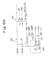
- Figures 10A and 10B are circuit diagrams indicating an example of a signal generating circuit in the non-volatile semiconductor memory device shown in Fig. 3, more particularly, an example of the signal generation circuit 410 shown in Fig. 3.
- the signal generation circuit 410 comprises circuit portions 4101, 4102, and 4103, and a plurality of signals output from the signal generation circuit 410 are applied to the memory portion 406 through the write data signal generation circuit 600.
- references TS1 to TS5 denote timing signals output from a timing signal generator (not shown).
- the control signals SEL L and SEL R which are output signals of the circuit portion 4102, are used in the embodiment of the non-volatile semiconductor memory device shown in Fig. 12, and the control signals CSEL L and CSEL R , which are output signals of the circuit portion 4103, are used in the embodiment of the non-volatile semiconductor memory devices shown in Figs. 12 and 13.
- these circuit portions 4101, 4102, and 4103 indicate an exampel, and a plurality of circuit configurations can be provided.
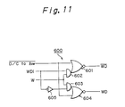
- Figure 11 is a logic diagram indicating an embodiment of a circuit for producing write data signals in the non-volatile semiconductor memory device shown in Fig. 3, more particularly, an embodiment of the write data signal generation circuit 600 shown in Fig. 3.
- the write data signal generation circuit 600 is used to generate signals (write data signal WD and WD ) to be applied to write data lines WD and WD .
- the write data signal generation circuit 600 comprises AND-NOR complexed gates 601(602), 604(603), and an inverter 605, and the write data signal generation circuit 600 generates the write data signal WD and WD from a write signal W, an input signal WDI and timing signal D/C to low .
- the signal D/C to low is specified to force the write data signal WD and WD inactive state (high level) at the end of write/erase operation.
- access time is limitted the long seting time of the bias voltage V B in the prior art non-volatile semiconductor memory devices
- an effective capacitance load at the bias voltage V B can be reduced in accordance with source to gate feedback of transistors 161, 162, whereas access time can be shortened.
- write/erase for each indvidual bit can be carried out in one operation, so that deterioration of the cell transistor can be decreased.
- Figure 12 is a circuit diagram indicating another embodiment of a non-volatile semiconductor memory device according to the present invention. Comparing the non-volatile semiconductor memory devices shown in Figs. 4 and 11, in the non-volatile semiconductor memory device of Fig. 12, a drain column line DCL, a control column line CCL, and a source column line SCL are divided into two groups which can be selected by select signals SEL L , SEL R . Note, each of the two groups includes an EEPROM cell 1 L , or 1 R . Note, in the non-volatile semiconductor memory device shown in Fig. 12, the same configurations in the non-volatile semiconductor memory device shown in Fig. 4 are indicated by the same references described in Fig. 4.
- a write stabilizing circuit 6′ comprises transistors controlled by the select signals SEL L , SEL R , and transistors 64 L , 64 R whose gate terminals are connected to a write data WD corresponding to the transistor 64 in the write stabilizing circuit 6 shown in Fig. 4. Consequently, two source column lines SCL L , SCL R , which can be selected by the select signals SEL L , SEL R , are provided.
- each of the EEPROM cells 1 L and 1 R is the same configuration as the cell explained with reference to Fig. 4. Further, enhancement type transistors 171, 172 are used to protect a sense circuit 5 from high voltages (for example, over 18 volts) applied to the drain column line DCL and the control column line CCL.
- EEPROM cells as in the non-volatile semiconductor memory device shown in Fig. 4 can be driven by the same number of sense circuits 5, the write stabilizing circuits 6′, the pump circuits 71, 72, and a pair of control lines 21, 22 (drain column line DCL and control column line CCL) as in that shown in Fig. 4.
- the two EEPROM cells 1 L and 1 R are provided for each word select line WSL and the same sense circuit 5, the same write stabilizing circuit 6′, the same pump circuit 71, 72, and the same pair of control lines 21, 22 are also provided, however a plurality of EEPROM cells (n pieces) can be provided for the same sense circuit 5, the same pair of control lines 21, 22, and the like.
- Figure 13 is a circuit diagram indicating still another embodiment of a non-volatile semiconductor memory device according to the present invention.
- the non-volatile semiconductor memory devices shown in Fig 13 comprises a decoder portion 190.
- the decoder portion comprises four blocks 190a to 190d, and one block of the four blocks is selected in accordance with signals Ai, Ai , Ai ⁇ 1, Ai ⁇ 1 .
- a write stabilizing circuit 6 or 6′ provided in that shown in Figs. 4 or 11 can be deleted.
- one sense circuit 5 is corrected to four blocks, and each block (for example, block 190a) includes two group of column lines, so that eight dummy cells (or eight group of column lines) can be connected in accordance with select signals Ai, Ai , Ai ⁇ 1, Ai ⁇ 1 , and CSEL L , CSEL R .
- a plurality of EEPROM cells each including a cell transistor 11 and a control gate 12 are provided in the non-volatile semiconductor memory device, however they are not shown in Fig. 13.
- transistors 191 to 194 and an inverter 195 are provided, and a signal WDI is applied to a gate of the transistor 191 and an inverted signa of the signal WDI is applied to a gate of the transistor 193 through the inverter 195.
- gates of the transistors 192 and 193 are applied with a write signal W.
- an EEPROM cell which includes a control gate made of single polycrystal line silicon sufficient area, making it possible to write at a comparatively low voltage, and having a high degree of write repeatability, is preferable, because a drain column line DCL (or DCL L , DCL R ), a control column line CCL (CCL L , CCL R ), and a source column line SCL (SCL L , SCL R ) are required for the non-volatile semiconductor memory device of the present invention.
- the drain column line DCL, the control column line CCL, and the source column line SCL can be wired above the area occupied by the EEPROM cells, so that the occupied area of the EEPROM cells can be effectively usable.
- FIG. 14A is a block diagram indicating an example of a non-volatile semiconductor memory device according to the present invention.
- a non-volatile semiconductor memory device (EEPROM chip) of the present invention is formed in a single semiconductor body 200 and the non-volatile semiconductor memory device 200 comprises: a memory cell array 201, a sense and write amplifier 205, and a dummy cell 211, which all correspond to the non-volatile semiconductor memory device shown in Fig. 4.
- the non-volatile semiconductor memory device 200 comprises a high voltage generation circuit 202, an address buffer 203, a column select gates 204, a row decoder 206, a dummy word decoder 207, a column decoder 208, a data I/O portion 209, a timing generator 210, a control signal buffer 212, a control logic circuit 213.
- the high voltage generation circuit 202 corresponds to the booster circuit 402, the constant-voltage circuit 403, and the waveform shaping circuit 404 in the high voltage generation portion 400 shown in Fig. 3.
- the high voltage generation circuit 202 is connected to the sense and write amplifier 205 (sense circuit5) to apply a high voltage to the EEPROM cell array 201 (EEPROM cell 1).
- the address buffer 203 is connected to the column decoder 208, the row decoder 206, and the dummy word decoder 207.
- the data I/O portion 209 is corrected to the sense and write amplifier 205 to input and output data.
- the control signal buffer 212 receives control signals.
- the control logic circuit 213 is connected to the control signal buffer 212 to control the state (read state, write/erase state) of the non-volatile semiconductor memory device 200.
- the non-volatile semiconductor memory device further comprises a threshold voltage measuring column 216, a threshold voltage measuring terminal 214, and data input/output portion 215.
- Figure 14B is a circuit diagram indicating a threshold measuring portion of the non-volatile semiconductor memory device shown in Fig. 14A.
- the threshold voltage measuring column 216 includes a test dummy cell transistor (dummy cell) 211a and a test sense circuit (205a) to estimate a threshold voltage of a cell transistor (11) in the EEPROM cell arry 201 by applying a gate voltage of the test dummy cell transistor 211a.
- the threshold voltage measuring terminal 214 is connected to the threshold voltage measuring column 216 (or a gate of the test dummy cell 211a) to apply various voltages.
- a drain of the test dummy cell 211a is connected to a test control column line (CCL T ) through a transfer gate 132a.
- the threshold voltage measuring I/O portion 215 is connected to the test sense circuit 205a for inputting or detecting data to the threshold voltage of the cell transistor 11 (with reference to Fig. 14A), when applying various voltages to the threshold voltage measuring terminal 214.
- FIG. 15 is a block diagram indicating an example of a micro-controller including a non-volatile semiconductor memory device according to the present invention.
- the non-volatile semiconductor memory device (EEPROM) of the present invention can be provided in the micro-controller, which is used for on-vehicle equipment (e.g., for setting control parameters or codes suitable for an application environment), a measuring apparatus, a camera, a telephone set (e.g., for storing telephone numbers), a telemetering system, a fuzzy control apparatus, and the like.
- the micro-controller 300 which is formed in a single semiconductor body, comprise a central processing unit core (CPU core) 301, an input/output port (I/O port) 305, 309, and EEPROM portion 301 corresponding to the non-volatile semiconductor memory device of the present invention. Furthermore, the micro-controller 300 comprises a read only memory (ROM) 303, a random access memory (RAM) 304, a serial interface (serial I/F) 306, a timer 307, a serial port 308, an asynchronous I/O port 310, an analog circuit 311, and an analog port 312.
- ROM read only memory
- RAM random access memory
- serial I/F serial interface
- timer 307 a timer 307
- serial port 308 an asynchronous I/O port 310
- the EEPROM portion 301, the ROM 303, the RAM 304 are connected to the CPU core 302 and are controlled thereby, and the I/O ports 305, 308, 309, 310, the I/F 306, the timer 307 are connected to the CPU core 302 and input, output, or transfer data or signals for the CPU core 302. Further, the analog circuit 311 and the analog port 312 are used to directly input and output analog signals between the micro-controller 300 and an external device.
- an EEPROM cell, a dummy cell and a sense circuit are operatively connected to a drain column line and a control column line, and the sense circuit reads out the content written in the EEPROM cell by the difference between a current flowing through the EEPROM cell from the drain column line and a current flowing through the dummy cell from the control column line, so that write/erase of data for each one bit can be carried out in one operation. Therefore, in the non-volatile semiconductor memory device of the present invention, each required one bit can be written/erased in one operation, the same as in a general DRAM, and deterioration of a cell transistor can be decreased.
- an EEPROM cell transistor and a dummy cell transistor are formed in the same wafer processes of producing the non-volatile semiconductor memory device, so that threshold voltages Vth of the EEPROM cell transistor and the dummy cell transistor are changed in the same way when these threshold voltages Vth are fluctuated.
Landscapes
- Read Only Memory (AREA)
- Semiconductor Memories (AREA)
- Non-Volatile Memory (AREA)
Abstract
Consequently, write/erase operations of data for each one bit can be carried out in one operation, and access time can be shortened and deterioration of a cell transistor can be decreased in a read-out operation.
Description
- The present invention relates to a non-volatile semiconductor memory device, more particularly, to a non-volatile semiconductor memory device using an electrically erasable programmable read only memory (EEPROM) cell, a dummy cell, and a sense circuit.
- Recently, EEPROMs, which can be reprogrammed by electrically erasing the contents previously programmed therein, have come to be preferred over EPROMs which are erased by being irradiates with ultraviolet light. For example, an EEPROM can be used for on-vehicle equipment (e.g., for setting control parameters or codes suitable for an application environment), a measuring apparatus, a camera, a telephone set (e.g., for storing telephone numbers), a telemetering system, a fuzzy control apparatus, and the like. Generally, in the EEPROM, a plurality of bits of a specific group (for example, each column unit, or each word unit) are erased together, and thus a non-volatile semiconductor memory device (EEPROM), which enables a read/erase operation of only one required bit in one operation (operation cycle), is required.
- For example, a non-volatile semiconductor memory device according to the prior art comprises an EEPROM cell, transfer gates for selecting the EEPROM cell in response to a select signal applied to a word select line WSL, a write/erase circuit, and a current sense type sense circuit. The EEPROM cell includes a control electrode, a floating gate, a drain, and a source.
- Further, in the prior art, a non-volatile semiconductor memory device using a differential sense circuit has been proposed in "An Experimental 5-V-Only 256-kbit CMOS EEPROM with a High-Performance Single-Polysilicon Cell" (IEEE JOURNAL OF SOLID-STATE CIRCUITS, VOL. SC-21.
No 5. OCTOBER 1986). - Note, in these non-volatile semiconductor memory devices (EEPROMs), a plurality of bits of a specific group (for example, each column unit, or each word unit) are erased, and an erase cycle and a write cycle are carried out individually, so that the required time for a rewriting operation becomes long. Further, since the cell to be written into is previously erased and is then rewritten the cell itself is deteriorated.
Furthermore, in a non-volatile semiconductor memory device using a differential sense circuit according to the prior art, the required time for a rewriting operation becomes long and cells are deteriorated in a short time, because an erase operation and a write operation are individually carried out. - In addition, in the prior art, a plurality of single polysilicon EEPROM cells are developed and provided. For example, such single polysilicon EEPROM cells are disclosed in Japanese Unexamined Patent Publication (Kokai) No. 59-155968 (corresponding to U.S. Patent No. 4,642,673), Japanese Unexamined Patent Publication (Kokai) No. 63-156361 (corresponding to U.S. Patent No. 4,807,003), Japanese Unexamined Patent Publication (Kokai) No. 63-166274, and the like. These single polysilicon EEPROM cells can be used in a non-volatile semiconductor memory device according to the present invention.
- It is an object of the present invention to provide a non-volatile semiconductor memory device having high performance operation characteristics without being influenced by the fluctuations of threshold voltages of a cell transistor and a dummy cell. Further, it is another object of the present invention to provide a non-volatile semiconductor memory device enabling a write/erase operation of each one bit in one operation.
- According to the present invention, there is provided a non-volatile semiconductor memory device comprising: a first and second signal lines; a memory cell, operatively connected to the first and second signal lines, for storing data; a dummy cell, operatively connected to the first and second signal lines; and a sense circuit, for amplifying the difference between a potential of the first signal line and a potential of the second signal line; wherein, when a first current flowing through the memory cell from the first signal line, in response to data stored in the memory cell, is larger than a second current flowing through the dummy cell from the second signal line at a read-out operation, the second current is decreased; and when the first current is smaller than the second current at the read-out operation, the second current is increased.
- Furthermore, according to the present invention, there is also provided a micro-controller formed in a single semiconductor body comprising: a central processing unit core; an input/output port, connected to the central processing unit core, for inputting and outputting data and signals; a memory portion, connected to the central processing unit core, for writing, erasing, and reading out data in accordance with the control of the central processing unit core. The memory portion may comprise: a first and second signal lines; a memory cell, operatively connected to the first and second signal lines, for storing data; a dummy cell, operatively connected to the first and second signal lines; and a sense circuit, for amplifying the difference between a potential of the first signal line and a potential of the second signal line; wherein, when a first current flowing through the memory cell from the first signal line, in response to data stored in the memory cell, is larger than a second current flowing through the dummy cell from the second signal line at a read-out operation, the second current is decreased; and when the first current is smaller than the second current at the read-out operation, the second current is increased.
- The non-volatile semiconductor memory device may further comprise: a first and second transfer gates, provided between the memory cell and the first and second signal lines; a word select line, applied with a word select signal for controlling the first and second transfer gates; a third and fourth transfer gates, provided between the dummy cell and the first and second signal lines; and a dummy word select line, applied with a dummy word select signal for controlling the third and fourth transfer gates. A gate of the dummy cell may be connected to the first signal line through the third transfer gate, a drain thereof may be connected to the second signal line through the fourth transfer gate, and a source thereof may be connected to the ground through a fifth transfer gates controlled by a read control signal.
- Further, the non-volatile semiconductor memory device may further comprise a write stabilizing circuit, connected to the first and second signal lines, for improving reliability at a write operation, and an output line of the write stabilizing circuit is connected to the memory cell. The output line of the write stabilizing circuit may be connected to the ground through a sixth transfer gate controlled by a read control signal. The non-volatile semiconductor memory device may further comprise a first high-voltage switching circuit connected to the first signal line and a second high-voltage switching circuit connected to the second signal line, for boosting and applying a write/erase power supply voltage between the first and second signal lines by using a pumping clock signal.
- The memory cell may comprise: a cell transistor, including a floating gate, a drain connected to the first signal line through the first transfer gate, and a source connected to an output line of a write stabilizing circuit, for storing data by injecting electrons into the floating gate; and a control gate, including a control electrode connected to the second signal line through the second transfer gate, and a floating electrode connected to the floating gate of the cell transistor.
- The cell transistor and the dummy cell may be formed at the same size. A gate length and a gate width of the dummy cell may be formed the same as a gate length and a gate width of the cell transistor. A gate length of the dummy cell may be determined in accordance with the characteristics of the cell transistor. The cell transistor and the dummy cell may be formed in the same processes of producing the non-volatile semiconductor memory device. The memory cell may include a single polycrystal line silicon layer of a large occupied area, and the first and second signal lines may be wired above the area occupied by the memory cell. The memory cell may be an EEPROM cell.
- The sense circuit may be a differential type sense amplifier. The sense circuit may be connected to the first and second signal lines through a seventh and eighth transfer gates with a bias voltage applied thereto. The sense circuit may be used to write specific data into the the memory cell.
- The first and second signal lines and an output line of a write stabilizing circuit may be plurally provided, the memory cell may be plurally provided in parallel to each group of the first and second signal lines and the output lines of the write stabilizing circuit through a select circuit, and one of the plurality of memory cells may be selected in response to select signals applied to the select circuit.
- The non-volatile semiconductor memory device may further comprise: a high voltage generation portion for applying a high voltage to the memory cell; an address latch circuit for latching input and output addresses; and a data latch circuit for latching input and output data. The non-volatile semiconductor memory device may be formed in a single semiconductor body and the non-volatile semiconductor memory device may further comprise: a high voltage generation circuit, connected to the sense circuit, for applying a high voltage to the memory cell; an address buffer, connected to a column decoder, a row decoder, and a dummy word decoder, for inputting and outputting addresses; a data input/output portion connected to the sense circuit, for inputting and outputting data; and a control signal buffer for receiving control signals; and a control logic circuit, connected to the control signal buffer, for controlling the state of the non-volatile semiconductor memory device.
- The non-volatile semiconductor memory device may further comprise: a threshold voltage measuring column including a test dummy cell and a test sense circuit, for estimating a threshold voltage of the memory cell by measuring the test dummy cell, a threshold voltage measuring terminal, connected to the threshold voltage measuring column, for applying various voltages, and a threshold voltage measuring input/output portion, connected to the test sense circuit, for inputting or detecting data to measure the threshold voltage of the memory cell when applying various voltages to the threshold voltage measuring terminal.
- The present invention will be more clearly understood from the description of the preferred embodiments as set forth below with reference to the accompanying drawings, wherein:
- Figure 1 is a circuit diagram indicating an example of a non-volatile semiconductor memory device according to the prior art;
- Figure 2 is a diagram indicating a principle of a non-volatile semiconductor memory device according to the present invention;
- Figure 3 is a diagram indicating a overall configuration of an example of a non-volatile semiconductor memory device applying the present invention;
- Figure 4 is a circuit diagram indicating an embodiment of a non-volatile semiconductor memory device according to the present invention;
- Figure 5 is a diagram indicating an example of programming-inhibiting characteristics of the EEPROM cell;
- Figures 6A and 6B are circuit diagrams indicating the EEPROM cell and the dummy cell of the non-volatile semiconductor memory device shown in Fig. 4;
- Figures 7A to 7D are diagrams indicating configurations of the EEPROM cell and the dummy cell of the non-volatile semiconductor memory device shown in Fig. 4;
- Figure 8 is a waveform diagram for explaining a read out operation in the non-volatile semiconductor memory device shown in Fig. 4;
- Figure 9 is a waveform diagram for explaining a write/erase operation in the non-volatile semiconductor memory device shown in Fig. 4;
- Figures 10A and 10B are circuit diagrams indicating an example of a signal generating circuit in the non-volatile semiconductor memory device shown in Fig. 3;
- Figure 11 is a logic circuit diagram indicating an example of a circuit for producing write data signals in the non-volatile semiconductor memory device shown in Fig. 3;
- Figure 12 is a circuit diagram indicating another embodiment of a non-volatile semiconductor memory device according to the present invention;
- Figure 13 is a circuit diagram indicating still another embodiment of a non-volatile semiconductor memory device according to the present invention;
- Figure 14A is a block diagram indicating an example of a non-volatile semiconductor memory device according to the present invention;
Figure 14B is a circuit diagram indicating a dummy cell portion in a threshold measuring portion of the non-volatile semiconductor memory device shown in Fig. 14A; and - Figure 15 is a block diagram indicating an example of a micro-controller including a non-volatile semiconductor memory device according to the present invention.
- For a better understanding of the preferred embodiments, the problems of the prior art will be explained, with reference to Fig. 1.
- Figure 1 is a circuit diagram indicating an example of a non-volatile semiconductor memory device (EEPROM) according to the prior art. The EEPROM can be reprogrammed by electrically erasing the contents previously programmed in the EEPROM.
- As shown in Fig. 1, a non-volatile semiconductor memory device comprises an
EEPROM cell 801,transfer gates 831, 832 for selecting theEEPROM cell 801 in response to a select signal applied to a word select line WSL, a readbias generation circuit 800 for generating a bias voltage used in a read out operation, a write/erasecircuit 802, and a current sensetype sense circuit 805. Further, the non-volatile semiconductor memory device comprises:gate transistors cell 801 and thesense circuit 805; andtransistors inverter 853 for erasing the contents written in a specific numbers ofEEPROM cells 801 in response to an erase signal. Note, in theEEPROM cell 801, a reference 801a denotes a control electrode, 801b denotes a floating gate, 801c denotes a drain, and 801d denotes a source. As described above, the non-volatile semiconductor memory device shown in Fig. 1 uses the current sensetype sense circuit 805 without using a dummy cell, and write/erase/read-out operations are carried out thereby. Note, in this non-volatile semiconductor memory device, a plurality of bits of a specific group (for example, each column unit, or each word unit) are erased. - As described above, in the non-volatile semiconductor memory device shown in Fig. 1, a latch operation must be carried out when writing data to the
EEPROM cell 801, however, write/erase/read-out operations are carried out by using a current sensetype sense circuit 805. Further, in the non-volatile semiconductor memory device shown in Fig. 1, abias generation circuit 800, which is used to generate a bias voltage for applying to a gate (control electrode 801a) of anEEPROM cell 801 at the read-out operation, must be provided. Therefore, a time for setting the bias voltage output from thebias generation circuit 800 becomes an obstruction to high speed access. Furthermore, in the non-volatile semiconductor memory device, an erase cycle (about 10 msec.) and a write cycle (about 10 msec.) are individually carried out, and thus the required time for a rewriting operation becomes long, i.e., determined at about 20 msec. In addition, the cell to be written is previously erased and it is rewritten thereafter, and thus the cell deteriorates at double the speed in worst case. Namely, in the non-volatile semiconductor memory device according to the prior art, the required time for a rewriting operation becomes long and cells are deteriorated in a short time, because an erase operation and a write operation are individually carried out. - Note, in the existing technique of producing a semiconductor device, a threshold voltage Vth of an EEPROM cell may by fluctuated by the processes of producing the EEPROM cell on a semiconductor substrate.
- Namely, when the threshold voltage Vth of the EEPROM cell is fluctuated, a read out operation cannot be exactly carried out.
- Next, a principle of a non-volatile semiconductor memory device according to the present invention will be explained, with reference to Fig. 2.
- Figure 2 is a diagram indicating a principle of a non-volatile semiconductor memory device according to the present invention. As shown in Fig. 2, the non-volatile semiconductor memory device of the present invention comprises a first and
second control lines 21, 22 (or a drain column line DCL, and a control column line CCL), anEEPROM cell 1, adummy cell 101, and asense circuit 5. - The first and
second control lines
TheEEPROM cell 1 is connected to the first andsecond control lines second transfer gates second transfer gates select line 4. Thedummy cell 101 is connected to the first andsecond control lines fourth transfer gates fourth transfer gates select line 104. Thesense circuit 5 is connected to the first andsecond control lines EEPROM cell 1 by the difference between a current (Ir) flowing through theEEPROM cell 1 from thefirst control line 21 and a current (Id) flowing through thedummy cell 101 from thesecond control line 22. Note, the sense circuit is also used to write data into theEEPROM cell 1. - According to the non-volatile semiconductor memory device having the above configuration, write/erase/read-out operations of data for each one bit can be carried out in one operation (operation cycle). Therefore, in the non-volatile semiconductor memory device of the present invention, each required one bit can be written or erased in one operation, individually, the same as in a general DRAM, so that deterioration of a cell transistor can be decreased. Furthermore, in the non-volatile semiconductor memory device according to the present invention, an EEPROM cell transistor (11) and a dummy cell transistor (or dummy cell 101) are formed in the same processes of producing the non-volatile semiconductor memory device, so that threshold voltages of the EEPROM cell transistor and the dummy cell transistor are changed the same as when these threshold voltages are fluctuated by the wafer processes deviation of the non-volatile semiconductor memory device.
- Below, the preferred embodiments of a non-volatile semiconductor memory device according to the present invention will be explained, with reference to the accompanying drawings.
- Figure 3 is a diagram indicating a overall configuration of an example of a non-volatile semiconductor memory device applying the present invention, concretely, Fig. 3 indicates a system configuration for writing an EEPROM cell. As shown in Fig. 3, the system of the non-volatile semiconductor memory device comprises: a
memory portion 406 including an EEPROM cell, a decoder, a driver and a sense amplifier; a high voltage generation portion 400 for applying a high voltage (for example, about 12∼ 23 volts sufficiently higher than the normal power supply voltage) to thememory portion 406; awrite timer 407; anaddress latch circuit 408; adata latch circuit 409; a controlsignal generation circuit 410; and a write datasignal generation circuit 600. - The high voltage generation portion 400 comprises: a voltage
doubler rectifier circuit 401 for doubling an input power supply voltage Vcc; abooster circuit 402 for boosting an output of the voltagedoubler rectifier circuit 401; a constant-voltage circuit 403 for stabilizing an output of thebooster circuit 402; awaveform shaping circuit 404 for waveform-shaping of an output of the constant-voltage circuit 403 in order to prevent a deterioration of a tunnel oxide film of an EEPROM cell; and a power-off/voltage-drop detection circuit 405. Note, thewaveform shaping circuit 404 is used to waveform-shape the output of the constant-voltage circuit 403, and thewrite timer 407 is used to stop the high voltage after a predetermined time by applying the output signal of thewrite timer 407 to the high voltage generation portion 400. Further, the high voltage is applied to thememory portion 406, and data applied to thedata latch circuit 409 are written to the addresses of thememory portion 406 corresponding to address signals applied to theaddress latch circuit 408. In addition, the power-off/voltage-drop detection circuit 405 is used to detect a power failure (for example, a cut off of a power supply and a drop of a voltage) during a write operation, and is used to output the result whether the write operation is exactly carried out or not. - Note, the non-volatile semiconductor memory device of the present invention particularly relates to the configuration of the
memory portion 406. - Figure 4 is a circuit diagram indicating an embodiment of a non-volatile semiconductor memory device according to the present invention. As shown in Fig. 4, in the non-volatile semiconductor memory device, an
EEPROM cell 1 is connected to a drain column line DCL (21) and a control column line CCL (22) throughtransfer gates transfer gates 31 and 32 (gates of thetransfer gates 31 and 32) are applied with a word select signal by a wordselect line 4. - The drain column line DCL is connected to a gate of a
dummy cell transistor 101 through agate transistor 131, and the control column line CCL is connected to a drain of thedummy cell transistor 101 through atransistor 132. Note, a source of thedummy cell transistor 101 is connected to the ground through atransistor 122 which is controlled by a read-out control signal R. Further, thetransistors - Furthermore, pump circuits (high-voltage switching circuits) 71 and 72, which are used to apply a high voltage (for example, about 7 ∼ 30 volts) between the drain column line DCL and the control column line CCL when write and erase operations are carried out, are provided to the drain column line DCL or the control column line CCL, respectively. Note, these
pump circuits write stabilizing circuit 6 is provided between the the drain column line DCL and the control column line CCL. Thiswrite stabilizing circuit 6 is constituted bytransistors 61 ∼ 64, and gates of thetransistors WD) each applying write data WD andWD . A connection portion between thetransistors EEPROM cell 1. Note, this source column line SCL is connected to the ground through atransistor 121 which is controlled by the dummy word select line DWL. - In addition, a sense circuit (differential type sense amplifier) 5 is connected to the drain column line DCL and the control column line CCL at nodes N₁ and N₂ through
transistors sense circuit 5, and an ground potential is applied to thesense circuit 5 through atransistor 110 which is controlled by a latch enable signal LE. Namely, read out data RD andRD , which are output frominverters sense circuit 5 reads out the content written in theEEPROM cell 1 by the difference between a current flowing in the control column line CCL through the dummy cell (dummy cell transistor) 101 and a current flowing in the drain column line DCL through theEEPROM cell 1. Note, the levels of the node N₁ and the drain column line DCL are inverted levels of the node N₂ and the control column line CCL. - The
EEPROM cell 1 comprises acell transistor 11 and acontrol gate 12. Thecell transistor 11 includes a single polycrystal silicon layer (floating gate), adrain 111 of thecell transistor 11 is connected to the drain column line DCL through atransfer gate 31, and asource 113 thereof is directly connected to the source column line SCL. Further, a gate (floating gate) 112 of thecell transistor 11 is connected to an electrode (floating electrode) 12b opposite to acontrol electrode 12a of thecontrol gate 12. Note, thecontrol electrode 12a is constituted by a diffusion region formed close to a surface of a semiconductor substrate. - In the above descriptions, the
cell transistor 11 of theEEPROM cell 1 and the dummy cell (dummy cell transistor) 101 can be formed at the same size. Namely, a gate length (Ld) and a gate width (Wd) of thedummy cell 101 are formed the same as a transistor length (or a gate length Lr) and a transistor width (or a gate width Wr) of thecell transistor 11. In this case, both currents (Ide, Idw) of an erased and written states flowing through thedummy cell 101 and the control column line CCL are determined within a current (Ire) of an erased state and a current (Irw) of a written state flowing through thecell transistor 11 and the drain column line DCL (with reference to Fig. 8). - Figure 5 is a diagram indicating an example of programming-inhibiting characteristics of the EEPROM cell. Generally, write characteristics of an EEPROM cell (1) are decreased in accordance with increasing the number of write/erase operations (rewriting number).
Namely, when the rewriting number becomes large, or the rewriting number is increased to about 10⁶ times (over 10⁴ times), the threshold difference between a written cell and an erased cell (cell transistor 11) becomes small. Note, this phenomenon (programming-inhibiting characteristics) is usually called Window Closing and is shown in Fig. 5. In Fig. 5, broken lines indicate another programming-inhibiting characteristics when a potential difference in a program cycle is larger than the programming-inhibiting characteristics indicated by solid lines. - Figures 6A and 6B are circuit diagrams indicating the EEPROM cell and the dummy cell of the non-volatile semiconductor memory device shown in Fig. 4, and Figs. 7A to 7D are diagrams indicating configurations of the EEPROM cell and the dummy cell of the non-volatile semiconductor memory device shown in Fig. 4. Note, Fig. 6A mainly indicate an
EEPROM cell 1 including acell transistor 11 and acontrol gate 12, and Fig. 6B mainly indicate adummy cell 101. Further, Fig. 7A is a plan view indicating theEEPROM cell 1, and Fig. 7B is a sectional view cut along a A-A line shown in Fig. 7A. Similarly, Fig. 7C is a plan view indicating thedummy cell 101, and Fig. 7D is a sectional view cut along a B-B line shown in Fig. 7C. In addition, in Figs. 7A to 7D, references 701 to 707 denote via holes passing through a layer, or contact holes connecting wirings (DCL, CCL) to a substrate, a diffusion region, or another wiring. - As described above, the
cell transistor 11 of theEEPROM cell 1 is preferably formed the same size as the dummy cell (dummy cell transistor) 101, namely, a gate length (Lr) and a gate width (Wr) of thecell transistor 11 can be formed the same as a gate length (Ld) and a gate width (Wd) of the dummy cell transistor 101 (with reference to Figs. 7A to 7D). In this case, a trans-conductance Gmc of thecell transistor 11 and a trans-conductance Gmd of thedummy cell transistor 101 can be specified as the same value. Note, a threshold voltage VFG of thecell transistor 1 corresponds to a threshold voltage VG of thedummy cell transistor 101 detected from thesense circuit 5, and thus the following equation (1) is valid in a critical condition (VFG > VFGcrit : written state; VFG < V FGcrit : erased state).
- Note, a charge Q corresponds to a threshold voltageshift. Next, assuming a threshold voltage Vtci of the
cell transistor 11, which is defined at the floatinggate 112 of thecell transistor 11, to be equal to the threshold voltage of thedummy cell transistor 101, a sense current Is is determined by the following equation (2).
- Note, in the equation (2), a relationship between the value of β and trans-conductance Gmc (Gmd) is determined by the following equation (3) in saturation region of the transistor operation, which is generally known.

- Therefore, the following equation (4) is obtained.

- When the cell transistor 11 (EEPROM cell 1) and the
dummy cell transistor 101 are formed at the same specific size, or when a gate length (Ld) and a gate width (Wd) of thedummy cell transistor 101 are formed the same as a gate length (Lr) and a gate width (Wr) of thecell transistor 11, for example, Vtci is specified as 0.2 volts, VccL is specified as 1.2 volts, and a capacitance ratio is specified as 0.71 (Ctot = 75.5 fF and Cc = 53.4 fF; f: Femto, or 10⁻¹⁵), and the sense current Is is to be 10 µ A, the written charge required to cause the critical condition is obtained as 26.3 x 10⁻¹⁵ Q from the above equations. - Note, the threshold voltage derived from written charge (26.3 x 10⁻¹⁵ Q) corresponds to a threshold change (for a write operation) Δ VFG = Q/Ctot = 0.49 volts. In the drawing of Window Closing shown in Fig. 5, a reference Vx (-0.49 volts) indicates the threshold voltage of the
sense circuit 5. Namely, as shown in Fig. 5, when thecell transistor 11 and thedummy cell transistor 101 are formed at the same size, the threshold voltaqe (Vx = -0.49 volts) is preferably positioned between the threshold voltage of a written cell and the threshold voltage of an erased cell (cell transistor 11). Consequently, even though the rewriting number is increased (over 10⁴ times) and the threshold difference between the written cell transistor and the erased cell transistor becomes small, erroneous operation is not easily caused. - Note, in the non-volatile semiconductor memory device according to the present embodiment, the
EEPROM cell transistor 11 and the dummy cell transistor 101 (dummy cell) are formed in the same wafer processes to produce the non-volatile semiconductor memory device, so that threshold voltages of theEEPROM cell transistor 11 and thedummy cell transistor 101 are changed as the same when these threshold voltages are fluctuated by deviating the wafer processing conditions from the standard. In the above embodiment, thecell transistor 11 and thedummy cell transistor 101 are formed at the same size, but in the present invention, the sizes of thecell transistor 11 and thedummy cell transistor 101 can be different therebetween. Namely, the gate length (Ld) and the gate width (Wd) of thedummy cell transistor 101 can be of different sizes from the gate length (Lr) and the gate width (Wr) of thecell transistor 11, in accordance with characteristics of thecell transistor 11 and thedummy cell transistor 101, especially, the gate length (Ld) thedummy cell transistor 101 can be determined in accordance with characteristics of thecell transistor 11. - Next, operations in the above described embodiment of the non-volatile semiconductor memory device will be explained.
- Figure 8 is a waveform diagram for explaining a read out operation in the non-volatile semiconductor memory device shown in Fig. 4.
- First, a read-out operation will be explained. As shown in Fig. 8, when a read-out control signal R is changed to a high level, both write data WD and
WD are changed to a low level, and then a precharge control signalPC is changed to an active state (low level), so that the nodes N₁ and N₂ are precharged at a potential of the power supply voltage Vcc. Next, a bias voltage VB is increased and it goes toward 1∼4 volts (for example, about 2.3 volts), and then, a word select line WSL and a dummy word select line DWL are selected (high levels). - When the precharge control signal
PC is changed to an inactive state (high level), a specific potential is caused between the control column line CCL and the drain column line DCL, or between the nodes N₁ and N₂. - Furthermore, when a latch enable signal LE is changed to an active state (high level), a sense operation (latch operation) in the
sense circuit 5 is settled and outputs of thesense circuit 5 are validated. Note, the outputs of thesense circuit 5 are brought out from read-out data lines RD andRD throughinverters
Note, in the present embodiment, an erased state is defined when electrons are injected into the floating gate of the EEPROM cell, and a written state is defined when the electrons are discharged from the floating gates of the specific EEPROM cells corresponding to the required bits. - Namely, with reference to Figs. 4 and 8, when the
cell transistor 11 is a written state, or when electrons are discharged from the floating gates of thecell transistor 11, a current Irw flowing through thecell transistor 11 from the drain column line DCL is increased, so that a potential of the node N₁ (drain column line DCL) is decreased to a low level. At the same time, the gate of thedummy cell transistor 101 is at the low level and a current Idw flowing through thedummy cell transistor 101 from the control column line CCL is decreased, and thus a potential of the node N₂ is increased to a high level which is limitted to a voltage at the control column line CCL of 1.2 volts at the maximum voltage by thetransistors RD is at a low level. - Conversely, when the
cell transistor 11 is an erased state, or when electrons are injected into the floating gate of thecell transistor 11, a current Ire flowing through thecell transistor 11 from the drain column line DCL is decreased (with reference to Figs. 4 and 8), so that a potential of the node N₁ is increased to a high level (for example, a voltage of the drain column line DCL is limitted to 1.2 volts at the maximum voltage by thetransistors dummy cell 101 is at the high level and a current Ide flowing through thedummy cell 101 from the control column line CCL is increased (with reference to Fig. 8), and thus a potential of the node N₂ (control column line CCL) is decreased to a low level. Consequently, the read-out data lineRD is at a low level, and the read-out data line RD is at a high level. - Note, as described above, when a current Ir (Irw) flowing through the cell transistor 11 (EEPROM cell 1) from the drain column line DCL is larger than a current Id (Idw) flowing through the dummy cell (transistor) 101 from the control column line CCL (which is the written state) at a read-out operation, the current Id (Idw) is decreased, so that the difference between a potential of the drain column line DCL and a potential of the control column line CCL becomes large. Note, the potential of the drain column line DCL is lower than that of the control column line CCL. Conversely, when a current Ir (Ire) flowing through the cell transistor 11 (EEPROM cell 1) from the drain column line DCL is smaller than a current Id (Ide) flowing through the dummy cell (transistor) 101 from the control column line CCL (which is the erased state) at the read-out operation, the current Id (Ide) is increased, so that the difference between a potential of the drain column line DCL and a potential of the control column line CCL becomes large. Note, the potential of the drain column line DCL is higher than that of the control column line CCL. Therefore, an erroneous operation is not easily caused, at the read-out operation.
- Further, a reset operation at the time of reading out will be briefly explained. First, the read-out control signal R is specified as a low level, the bias voltage VB is specified as a low level, both write data lines WD and
WD are specified as a high level, both the drain column line DCL and the control column line CCL are specified as a low level, and then the word select line WSL and the dummy word select line DWL are specified as a low level, so that the read-out operation is completed. - Next, definitions of write/erase will be described, and then, a write/erase operation in the non-volatile semiconductor memory device shown in Fig. 4 will be explained. When an erase operation is carried out, in the
EEPROM cell 1 shown in Fig. 4, acontrol electrode 12a of acontrol gate 12 is changed to a high level (high voltage), and both drain 111 andsource 113 of acell transistor 11 are held at a low level, so that a Fowler-Nordheim current flows through a tunnel oxide film 11a of thecell transistor 11 and electrons are injected into a floating gate (a gate 112). Consequently, a threshold voltage VTH of thecell transistor 11 against thecontrol electrode 12a is increased, and this state is defined as an erased state. - Figure 9 is a waveform diagram for explaining a write/erase operation in the non-volatile semiconductor memory device shown in Fig. 4.
- First, a write/erase operation will be explained. As shown in Fig. 9, the levels of write data lines WD and
WD are settled (note, addresses are also settled) by write data, and further, a bias voltage VB is increased, for example, the bias voltage VB is brought to the power supply voltage Vcc. Next, a latch enable signal LE is specified to an active state (high level). Furthermore, a voltage of one of a drain column line DCL and a control column line CCL, whose level is previously specified as a high level, is further increased to from about a few volts to 30 volts, by increasing a write/erase power supply voltage Vpp and by a function of pump circuits (high voltage switching circuits) 71, 72, so that the above described write operation (or, erase operation) is carried out. - Next, a reset operation will be explained. As shown in Fig. 9, the write data lines WD and
WD are fixed at high levels, a word select line WSL is specified as a low level, and the bias voltage VB is specified as a low level, so that one of the drain column line DCL and the control column line CCL which was the high level is changed to a low level. Furthermore, the latch enable signal LE and the write/erase power supply voltage Vpp are specified as low levels, so that the write/erase operation is completed. - Figures 10A and 10B are circuit diagrams indicating an example of a signal generating circuit in the non-volatile semiconductor memory device shown in Fig. 3, more particularly, an example of the
signal generation circuit 410 shown in Fig. 3. - As shown in Figs. 3,10A and 10B, the
signal generation circuit 410 comprisescircuit portions signal generation circuit 410 are applied to thememory portion 406 through the write datasignal generation circuit 600. Note, in Fig. 10A, references TS₁ to TS₅ denote timing signals output from a timing signal generator (not shown). Further, the control signals SELL and SELR, which are output signals of thecircuit portion 4102, are used in the embodiment of the non-volatile semiconductor memory device shown in Fig. 12, and the control signals CSELL and CSELR, which are output signals of thecircuit portion 4103, are used in the embodiment of the non-volatile semiconductor memory devices shown in Figs. 12 and 13. Note, thesecircuit portions - Figure 11 is a logic diagram indicating an embodiment of a circuit for producing write data signals in the non-volatile semiconductor memory device shown in Fig. 3, more particularly, an embodiment of the write data
signal generation circuit 600 shown in Fig. 3. - As shown in Fig. 11, the write data
signal generation circuit 600 is used to generate signals (write data signal WD andWD ) to be applied to write data lines WD andWD . The write datasignal generation circuit 600 comprises AND-NOR complexed gates 601(602), 604(603), and aninverter 605, and the write datasignal generation circuit 600 generates the write data signal WD andWD from a write signal W, an input signal WDI and timing signalD/C to low . Note, the signalD/C to low is specified to force the write data signal WD andWD inactive state (high level) at the end of write/erase operation. - Further, though access time is limitted the long seting time of the bias voltage VB in the prior art non-volatile semiconductor memory devices, according to the embodiment of the non-volatile semiconductor memory device shown in Fig. 4, an effective capacitance load at the bias voltage VB can be reduced in accordance with source to gate feedback of
transistors - Figure 12 is a circuit diagram indicating another embodiment of a non-volatile semiconductor memory device according to the present invention. Comparing the non-volatile semiconductor memory devices shown in Figs. 4 and 11, in the non-volatile semiconductor memory device of Fig. 12, a drain column line DCL, a control column line CCL, and a source column line SCL are divided into two groups which can be selected by select signals SELL, SELR. Note, each of the two groups includes an
EEPROM cell - Namely, as shown in Fig. 12, in the non-volatile semiconductor memory device according to the present embodiment, a
write stabilizing circuit 6′ comprises transistors controlled by the select signals SELL, SELR, andtransistors transistor 64 in thewrite stabilizing circuit 6 shown in Fig. 4. Consequently, two source column lines SCLL, SCLR, which can be selected by the select signals SELL, SELR, are provided. - Furthermore, in the non-volatile semiconductor memory device shown in Fig. 12, with regard to the drain column line DCL and the control column line CCL of the non-volatile semiconductor memory device shown in Fig. 4, two drain column lines DCLL, DCLR and two control column lines CCLL, CCLR, which can be selected by the select signals SELL, SELR through
transistors
Note, each of the two drain column lines DCLL, DCLR, two control column lines CCLL, CCLR, and two source column lines SCLL, SCLR are connected to each of twoEEPROM cells - Note, each of the
EEPROM cells enhancement type transistors sense circuit 5 from high voltages (for example, over 18 volts) applied to the drain column line DCL and the control column line CCL. - As described above, according to the non-volatile semiconductor memory device of the present embodiment, twice as many of EEPROM cells as in the non-volatile semiconductor memory device shown in Fig. 4 can be driven by the same number of
sense circuits 5, thewrite stabilizing circuits 6′, thepump circuits control lines 21, 22 (drain column line DCL and control column line CCL) as in that shown in Fig. 4. - Note, in the non-volatile semiconductor memory device shown in Fig. 12, the two
EEPROM cells same sense circuit 5, the samewrite stabilizing circuit 6′, thesame pump circuit control lines same sense circuit 5, the same pair ofcontrol lines - Figure 13 is a circuit diagram indicating still another embodiment of a non-volatile semiconductor memory device according to the present invention. As shown in Fig 13, the non-volatile semiconductor memory devices shown in Fig 13, comprises a
decoder portion 190. The decoder portion comprises four blocks 190a to 190d, and one block of the four blocks is selected in accordance with signals Ai,Ai , Ai₋ ₁,Ai₋₁ . Note, in the non-volatile semiconductor memory devices shown in Fig 13, awrite stabilizing circuit sense circuit 5 is corrected to four blocks, and each block (for example, block 190a) includes two group of column lines, so that eight dummy cells (or eight group of column lines) can be connected in accordance with select signals Ai,Ai , Ai₋ ₁,Ai₋ ₁ , and CSELL, CSELR. Note, a plurality of EEPROM cells each including acell transistor 11 and acontrol gate 12 are provided in the non-volatile semiconductor memory device, however they are not shown in Fig. 13. - In the non-volatile semiconductor memory devices shown in Fig 13,
transistors 191 to 194 and aninverter 195 are provided, and a signal WDI is applied to a gate of thetransistor 191 and an inverted signa of the signal WDI is applied to a gate of thetransistor 193 through theinverter 195. Note, gates of thetransistors - In the above three embodiments of the non-volatile semiconductor memory device according to the present invention, various types of EEPROM cells can be used. However, an EEPROM cell, which includes a control gate made of single polycrystal line silicon sufficient area, making it possible to write at a comparatively low voltage, and having a high degree of write repeatability, is preferable, because a drain column line DCL (or DCLL, DCLR), a control column line CCL (CCLL, CCLR), and a source column line SCL (SCLL, SCLR) are required for the non-volatile semiconductor memory device of the present invention. Namely, in the above non-volatile semiconductor memory device comprising the EEPROM cell including the single polycrystal line silicon layer of the large occupied area, and the like, the drain column line DCL, the control column line CCL, and the source column line SCL can be wired above the area occupied by the EEPROM cells, so that the occupied area of the EEPROM cells can be effectively usable.
- Figure 14A is a block diagram indicating an example of a non-volatile semiconductor memory device according to the present invention. As shown in Fig. 14A, a non-volatile semiconductor memory device (EEPROM chip) of the present invention is formed in a
single semiconductor body 200 and the non-volatilesemiconductor memory device 200 comprises: amemory cell array 201, a sense and writeamplifier 205, and adummy cell 211, which all correspond to the non-volatile semiconductor memory device shown in Fig. 4. Further, the non-volatilesemiconductor memory device 200 comprises a highvoltage generation circuit 202, anaddress buffer 203, a columnselect gates 204, arow decoder 206, adummy word decoder 207, acolumn decoder 208, a data I/O portion 209, atiming generator 210, acontrol signal buffer 212, acontrol logic circuit 213.
Note, the highvoltage generation circuit 202 corresponds to thebooster circuit 402, the constant-voltage circuit 403, and thewaveform shaping circuit 404 in the high voltage generation portion 400 shown in Fig. 3. - As shown in Fig. 14A, in the non-volatile semiconductor memory device, the high
voltage generation circuit 202 is connected to the sense and write amplifier 205 (sense circuit5) to apply a high voltage to the EEPROM cell array 201 (EEPROM cell 1). Theaddress buffer 203 is connected to thecolumn decoder 208, therow decoder 206, and thedummy word decoder 207. The data I/O portion 209 is corrected to the sense and writeamplifier 205 to input and output data. Thecontrol signal buffer 212 receives control signals. Thecontrol logic circuit 213 is connected to thecontrol signal buffer 212 to control the state (read state, write/erase state) of the non-volatilesemiconductor memory device 200. - Note, as shown in Fig. 14A, the non-volatile semiconductor memory device further comprises a threshold
voltage measuring column 216, a thresholdvoltage measuring terminal 214, and data input/output portion 215. - Figure 14B is a circuit diagram indicating a threshold measuring portion of the non-volatile semiconductor memory device shown in Fig. 14A. As shown in Fig. 14B, the threshold
voltage measuring column 216 includes a test dummy cell transistor (dummy cell) 211a and a test sense circuit (205a) to estimate a threshold voltage of a cell transistor (11) in the EEPROM cell arry 201 by applying a gate voltage of the testdummy cell transistor 211a. The thresholdvoltage measuring terminal 214 is connected to the threshold voltage measuring column 216 (or a gate of thetest dummy cell 211a) to apply various voltages. Note, a drain of thetest dummy cell 211a is connected to a test control column line (CCLT) through atransfer gate 132a. The threshold voltage measuring I/O portion 215 is connected to thetest sense circuit 205a for inputting or detecting data to the threshold voltage of the cell transistor 11 (with reference to Fig. 14A), when applying various voltages to the thresholdvoltage measuring terminal 214. - Figure 15 is a block diagram indicating an example of a micro-controller including a non-volatile semiconductor memory device according to the present invention. The non-volatile semiconductor memory device (EEPROM) of the present invention can be provided in the micro-controller, which is used for on-vehicle equipment (e.g., for setting control parameters or codes suitable for an application environment), a measuring apparatus, a camera, a telephone set (e.g., for storing telephone numbers), a telemetering system, a fuzzy control apparatus, and the like.
- Namely, as shown in Fig. 15, the
micro-controller 300, which is formed in a single semiconductor body, comprise a central processing unit core (CPU core) 301, an input/output port (I/O port) 305, 309, and EEPROM portion 301 corresponding to the non-volatile semiconductor memory device of the present invention. Furthermore, themicro-controller 300 comprises a read only memory (ROM) 303, a random access memory (RAM) 304, a serial interface (serial I/F) 306, atimer 307, aserial port 308, an asynchronous I/O port 310, ananalog circuit 311, and ananalog port 312. Note, the EEPROM portion 301, theROM 303, theRAM 304 are connected to theCPU core 302 and are controlled thereby, and the I/O ports F 306, thetimer 307 are connected to theCPU core 302 and input, output, or transfer data or signals for theCPU core 302. Further, theanalog circuit 311 and theanalog port 312 are used to directly input and output analog signals between the micro-controller 300 and an external device. - In accordance with a non-volatile semiconductor memory device according to the present invention as described above, an EEPROM cell, a dummy cell and a sense circuit are operatively connected to a drain column line and a control column line, and the sense circuit reads out the content written in the EEPROM cell by the difference between a current flowing through the EEPROM cell from the drain column line and a current flowing through the dummy cell from the control column line, so that write/erase of data for each one bit can be carried out in one operation. Therefore, in the non-volatile semiconductor memory device of the present invention, each required one bit can be written/erased in one operation, the same as in a general DRAM, and deterioration of a cell transistor can be decreased. Furthermore, in the non-volatile semiconductor memory device according to the present invention, an EEPROM cell transistor and a dummy cell transistor are formed in the same wafer processes of producing the non-volatile semiconductor memory device, so that threshold voltages Vth of the EEPROM cell transistor and the dummy cell transistor are changed in the same way when these threshold voltages Vth are fluctuated.
- Many widely differing embodiments of the present invention may be constructed without departing from the spirit and scope of the present invention, and it should be understood that the present invention is not limited to the specific embodiments described in this specification, except as defined in the appended claims.
Claims (22)
- A non-volatile semiconductor memory device including: a first and second signal lines (21,DCL; 22,CCL); and a memory cell (1), operatively connected to said first and second signal lines (21,DCL; 22,CCL), for storing data, characterized in that said non-volatile semiconductor memory device comprises:
a dummy cell (101), operatively connected to said first and second signal lines (21,DCL; 22,CCL); and
a sense circuit (5), for amplifying the difference between a potential of said first signal line (21,DCL) and a potential of said second signal line (22,CCL);
wherein, when a first current (Ir; Irw) flowing through said memory cell (1) from said first signal line (21,DCL), in response to data stored in said memory cell (1), is larger than a second current (Id;Idw) flowing through said dummy cell (101) from said second signal line (22,CCL) at a read-out operation, said second current (Id;Idw) is decreased; and when said first current (Ir;Ire) is smaller than said second current (Id;Ide) at the read-out operation, said second current (Id;Ide) is increased. - A non-volatile semiconductor memory device as claimed in claim 1, wherein said non-volatile semiconductor memory device further comprises:
a first and second transfer gates (31, 32), provided between said memory cell (1) and said first and second signal lines (21,DCL; 22,CCL);
a word select line (4,WSL), applied with a word select signal for controlling said first and second transfer gates (31, 32);
a third and fourth transfer gates (131, 132), provided between said dummy cell (101) and said first and second signal lines (21,DCL; 22,CCL); and
a dummy word select line (104,DWL), applied with a dummy word select signal for controlling said third and fourth transfer gates (131, 132). - A non-volatile semiconductor memory device as claimed in claims 1 or 2, wherein a gate of said dummy cell (101) is connected to said first signal line (21,DCL) through said third transfer gate (131), a drain thereof is connected to said second signal line (22,CCL) through said fourth transfer gate (132), and a source thereof is connected to the ground through a fifth transfer gates (122) controlled by a read control signal (R).
- A non-volatile semiconductor memory device as claimed in any one of the preceding claims, wherein said non-volatile semiconductor memory device further comprises a write stabilizing circuit (6), connected to said first and second signal lines (21,DCL; 22,CCL), for improving reliability at a write operation, and an output line (SCL) of said write stabilizing circuit (6) is connected to said memory cell (1).
- A non-volatile semiconductor memory device as claimed in claim 4, wherein said output line (SCL) of said write stabilizing circuit (6) is connected to the ground through a sixth transfer gate (121) controlled by a read control signal (R).
- A non-volatile semiconductor memory device as claimed in any one of the preceding claims, wherein said non-volatile semiconductor memory device further comprises a first high-voltage switching circuit (71) connected to said first signal line (21,DCL) and a second high-voltage switching circuit (72) connected to said second signal line (22,CCL), for boosting and applying a write/erase power supply voltage (Vpp) between said first and second signal lines (21,DCL; 22,CCL) by using a pumping clock signal (CLK,PHIPUMP).
- A non-volatile semiconductor memory device as claimed in any one of the preceding claims, wherein said memory cell (1) comprises:
a cell transistor (11), including a floating gate (112), a drain (111) connected to said first signal line (21,DCL) through said first transfer gate (31), and a source (113) connected to an output line (SCL) of a write stabilizing circuit (6), for storing data by injecting electrons into said floating gate (112); and
a control gate (12), including a control electrode (12a) connected to said second signal line (22,CCL) through said second transfer gate (32), and a floating electrode (12b) connected to said floating gate (112) of said cell transistor (11). - A non-volatile semiconductor memory device as claimed in claim 7, wherein said cell transistor (11) and said dummy cell (101) are formed at the same size.
- A non-volatile semiconductor memory device as claimed in claim 8, wherein a gate length (Ld) and a gate width (Wd) of said dummy cell (101) are formed the same as a gate length (Lr) and a gate width (Wr) of said cell transistor (11).
- A non-volatile semiconductor memory device as claimed in claim 7, wherein a gate length (Ld) of said dummy cell (101) is determined in accordance with the characteristics of said cell transistor (11).
- A non-volatile semiconductor memory device as claimed in claim 7, wherein said cell transistor (11) and said dummy cell (101) are formed in the same processes of producing said non-volatile semiconductor memory device.
- A non-volatile semiconductor memory device as claimed in claim 7, wherein said memory cell (1) includes a single polycrystal line silicon layer of a large occupied area, and said first and second signal lines (21,DCL; 22,CCL) are wired above the area occupied by said memory cell (1).
- A non-volatile semiconductor memory device as claimed in any one of the preceding claims, wherein said memory cell (1) is an EEPROM cell.
- A non-volatile semiconductor memory device as claimed in any one of the preceding claims, wherein said sense circuit (5) is a differential type sense amplifier.
- A non-volatile semiconductor memory device as claimed in any one of the preceding claims, wherein said sense circuit (5) is connected to said first and second signal lines (21,DCL; 22,CCL) through a seventh and eighth transfer gates (161, 162) with a bias voltage (VB) applied thereto.
- A non-volatile semiconductor memory device as claimed in any one of the preceding claims, wherein said sense circuit (5) is used to write specific data into said said memory cell (1).
- A non-volatile semiconductor memory device as claimed in any one of the preceding claims, wherein said first and second signal lines (21,DCL; 22,CCL) and an output line (SCL) of a write stabilizing circuit (6′) are plurally provided, said memory cell (1) is plurally provided in parallel to each group of said first and second signal lines (DCLL,DCLR; CCLL,CCLR) and said output lines (SCLL,SCLR) of said write stabilizing circuit (6′) through a select circuit (65L,65R; 181L,181R; 182L,182R), and one of said plurality of memory cells (1L, 1R) is selected in response to select signals (SELL, SELR) applied to said select circuit (65L,65R; 181L,181R; 182L,182R).
- A non-volatile semiconductor memory device as claimed in any one of the preceding claims, wherein said non-volatile semiconductor memory device further comprises: a high voltage generation portion (400) for applying a high voltage to said memory cell (1); an address latch circuit (408) for latching input and output addresses; and a data latch circuit (409) for latching input and output data.
- A non-volatile semiconductor memory device as claimed in any one of the preceding claims, wherein said non-volatile semiconductor memory device is formed in a single semiconductor body (200) and said non-volatile semiconductor memory device (200) further comprises: a high voltage generation circuit (202), connected to said sense circuit (5, 205), for applying a high voltage to said memory cell (1, 201); an address buffer (203), connected to a column decoder (208), a row decoder (206), and a dummy word decoder (207), for inputting and outputting addresses; a data input/output portion (209) connected to said sense circuit (5, 205), for inputting and outputting data; and a control signal buffer (212) for receiving control signals; and a control logic circuit (213), connected to said control signal buffer (212), for controlling the state of said non-volatile semiconductor memory device (200).
- A non-volatile semiconductor memory device as claimed in claim 19, wherein said non-volatile semiconductor memory device further comprises: a threshold voltage measuring column (216) including a test dummy cell and a test sense circuit, for estimating a threshold voltage of said memory cell (1, 201) by measuring said test dummy cell, a threshold voltage measuring terminal (214), connected to said threshold voltage measuring column (216), for applying various voltages, and a threshold voltage measuring input/output portion (215), connected to said test sense circuit, for inputting or detecting data to measure the threshold voltage of said memory cell (1, 201) when applying various voltages to said threshold voltage measuring terminal (214).
- A non-volatile semiconductor memory device as claimed in any one of the preceding claims, wherein said non-volatile semiconductor memory device is provided in a micro-controller (300) formed in a single semiconductor body including: a central processing unit core (302); and an input/output port (305, 309), connected to said central processing unit core (302), for inputting and outputting data and signals.
- A non-volatile semiconductor memory device as claimed in any one of the preceding claims, wherein said micro-controller (300) further comprises: an analog circuit (311) for directly inputting and outputting analog signals between said micro-controller and an external device.
Applications Claiming Priority (2)
| Application Number | Priority Date | Filing Date | Title |
|---|---|---|---|
| JP10751690A JP2933090B2 (en) | 1990-04-25 | 1990-04-25 | Nonvolatile semiconductor memory device |
| JP107516/90 | 1990-04-25 |
Publications (3)
| Publication Number | Publication Date |
|---|---|
| EP0454579A2 true EP0454579A2 (en) | 1991-10-30 |
| EP0454579A3 EP0454579A3 (en) | 1992-12-30 |
| EP0454579B1 EP0454579B1 (en) | 1996-10-16 |
Family
ID=14461182
Family Applications (1)
| Application Number | Title | Priority Date | Filing Date |
|---|---|---|---|
| EP91401092A Expired - Lifetime EP0454579B1 (en) | 1990-04-25 | 1991-04-24 | Non-volatile semiconductor memory device having EEPROM cell, dummy cell and sense circuit for increasing reliability and enabling one-bit operation |
Country Status (5)
| Country | Link |
|---|---|
| US (1) | US5303197A (en) |
| EP (1) | EP0454579B1 (en) |
| JP (1) | JP2933090B2 (en) |
| KR (1) | KR950011725B1 (en) |
| DE (1) | DE69122649D1 (en) |
Cited By (1)
| Publication number | Priority date | Publication date | Assignee | Title |
|---|---|---|---|---|
| EP0713164A1 (en) * | 1994-11-15 | 1996-05-22 | STMicroelectronics Limited | A reference circuit |
Families Citing this family (11)
| Publication number | Priority date | Publication date | Assignee | Title |
|---|---|---|---|---|
| US5592415A (en) | 1992-07-06 | 1997-01-07 | Hitachi, Ltd. | Non-volatile semiconductor memory |
| JP3132637B2 (en) * | 1995-06-29 | 2001-02-05 | 日本電気株式会社 | Nonvolatile semiconductor memory device |
| US5951702A (en) * | 1997-04-04 | 1999-09-14 | S3 Incorporated | RAM-like test structure superimposed over rows of macrocells with added differential pass transistors in a CPU |
| JP3027958B2 (en) * | 1997-05-26 | 2000-04-04 | 日本電気株式会社 | Circuit device and recording medium recording program |
| JP4081963B2 (en) | 2000-06-30 | 2008-04-30 | セイコーエプソン株式会社 | Storage device and access method for storage device |
| CA2326036A1 (en) * | 2000-11-16 | 2002-05-16 | Gemplus S.A. | Method for securing electronic device data processing |
| US6861715B2 (en) * | 2002-04-08 | 2005-03-01 | Guobiao Zhang | Electrically programmable three-dimensional memory |
| JP2004303342A (en) * | 2003-03-31 | 2004-10-28 | Toshiba Corp | Semiconductor storage device |
| US7577050B2 (en) * | 2005-09-29 | 2009-08-18 | Hynix Semiconductor, Inc. | Semiconductor memory device for measuring internal voltage |
| KR100897603B1 (en) * | 2007-06-20 | 2009-05-14 | 삼성전자주식회사 | Semiconductor memory device |
| US8458562B1 (en) * | 2008-12-30 | 2013-06-04 | Micron Technology, Inc. | Secondary memory element for non-volatile memory |
Family Cites Families (6)
| Publication number | Priority date | Publication date | Assignee | Title |
|---|---|---|---|---|
| JPS5931231B2 (en) * | 1980-01-31 | 1984-07-31 | 工業技術院長 | Floating gate non-volatile semiconductor memory |
| JPS59155968A (en) * | 1983-02-25 | 1984-09-05 | Toshiba Corp | Semiconductor memory device |
| US4807003A (en) * | 1986-12-19 | 1989-02-21 | National Semiconductor Corp. | High-reliablity single-poly eeprom cell |
| GB2199184B (en) * | 1986-12-19 | 1990-01-31 | Nat Semiconductor Corp | High reliability single-poly eeprom cell |
| IT1199828B (en) * | 1986-12-22 | 1989-01-05 | Sgs Microelettronica Spa | SINGLE LEVEL EEPROM MEMORY CELL WRITABLE AND CANCELLABLE POLYSILIC BIT A BIT |
| IT1228822B (en) * | 1989-03-23 | 1991-07-04 | Sgs Thomson Microelectronics | REFERENCE CELL FOR READING EEPROM MEMORY DEVICES. |
-
1990
- 1990-04-25 JP JP10751690A patent/JP2933090B2/en not_active Expired - Lifetime
-
1991
- 1991-04-24 EP EP91401092A patent/EP0454579B1/en not_active Expired - Lifetime
- 1991-04-24 US US07/690,482 patent/US5303197A/en not_active Expired - Fee Related
- 1991-04-24 DE DE69122649T patent/DE69122649D1/en not_active Expired - Lifetime
- 1991-04-25 KR KR1019910006685A patent/KR950011725B1/en not_active Expired - Fee Related
Non-Patent Citations (3)
| Title |
|---|
| IEEE JOURNAL OF SOLID-STATE CIRCUITS. vol. 20, no. 2, April 1985, NEW YORK US pages 603 - 608 CUPPENS ET AL. 'AN EEPROM FOR MICROPROCESSORS AND CUSTOM LOGIC' * |
| IEEE JOURNAL OF SOLID-STATE CIRCUITS. vol. 23, no. 5, October 1988, NEW YORK US pages 1150 - 1156 GASTALDI ET AL. 'A 1-MBIT CMOS EPROM WITH ENHANCED VERIFICATION' * |
| pages 1150 - 1156 GASTALDI ET AL. 'A 1-MBIT CMOS EPROM WITH ENHANCED VERIFICATION' * |
Cited By (2)
| Publication number | Priority date | Publication date | Assignee | Title |
|---|---|---|---|---|
| EP0713164A1 (en) * | 1994-11-15 | 1996-05-22 | STMicroelectronics Limited | A reference circuit |
| US5654918A (en) * | 1994-11-15 | 1997-08-05 | Sgs-Thomson Microelectronics Limited | Reference circuit for supplying a reference level for sensing in a memory |
Also Published As
| Publication number | Publication date |
|---|---|
| JPH047870A (en) | 1992-01-13 |
| EP0454579A3 (en) | 1992-12-30 |
| KR910019062A (en) | 1991-11-30 |
| EP0454579B1 (en) | 1996-10-16 |
| DE69122649D1 (en) | 1996-11-21 |
| US5303197A (en) | 1994-04-12 |
| JP2933090B2 (en) | 1999-08-09 |
| KR950011725B1 (en) | 1995-10-09 |
Similar Documents
| Publication | Publication Date | Title |
|---|---|---|
| US6031760A (en) | Semiconductor memory device and method of programming the same | |
| JP3373632B2 (en) | Nonvolatile semiconductor memory device | |
| US4903236A (en) | Nonvolatile semiconductor memory device and a writing method therefor | |
| KR100218244B1 (en) | Data reading circuit of nonvolatile semiconductor memory | |
| KR100349433B1 (en) | Semiconductor Memory Device | |
| JP2654596B2 (en) | Non-volatile storage device | |
| EP0454579B1 (en) | Non-volatile semiconductor memory device having EEPROM cell, dummy cell and sense circuit for increasing reliability and enabling one-bit operation | |
| KR100307114B1 (en) | Non volatile semiconductor memory, method for controlling the same, memory card and memory system | |
| US5347486A (en) | Nonvolatile memory device having self-refresh function | |
| US5617350A (en) | Flash memory system having reduced disturb and method | |
| KR910001185B1 (en) | Semiconductor memory device | |
| EP1324344B1 (en) | Sense amplifier structure for multilevel non-volatile memory devices and corresponding reading method | |
| KR930004488B1 (en) | Eeprom | |
| KR100222811B1 (en) | Nonvolatile semiconductor device | |
| EP1011105B1 (en) | One-chip microcomputer | |
| JP3862092B2 (en) | Nonvolatile memory device | |
| JP3505158B2 (en) | Nonvolatile semiconductor memory device | |
| JP2707521B2 (en) | Semiconductor device | |
| JP3722372B2 (en) | System and device having nonvolatile memory | |
| JP3197533B2 (en) | Semiconductor integrated circuit device and information processing system | |
| KR0176312B1 (en) | Information processing system using semiconductor integrated circuit device | |
| JP2719776B2 (en) | Semiconductor nonvolatile storage device | |
| JP2719775B2 (en) | Information processing system | |
| JPH02123598A (en) | Semiconductor nonvolatile memory device | |
| JP2001195891A (en) | Nonvolatile semiconductor memory device |
Legal Events
| Date | Code | Title | Description |
|---|---|---|---|
| PUAI | Public reference made under article 153(3) epc to a published international application that has entered the european phase |
Free format text: ORIGINAL CODE: 0009012 |
|
| AK | Designated contracting states |
Kind code of ref document: A2 Designated state(s): DE FR GB |
|
| PUAL | Search report despatched |
Free format text: ORIGINAL CODE: 0009013 |
|
| AK | Designated contracting states |
Kind code of ref document: A3 Designated state(s): DE FR GB |
|
| 17P | Request for examination filed |
Effective date: 19930611 |
|
| 17Q | First examination report despatched |
Effective date: 19950220 |
|
| GRAH | Despatch of communication of intention to grant a patent |
Free format text: ORIGINAL CODE: EPIDOS IGRA |
|
| GRAH | Despatch of communication of intention to grant a patent |
Free format text: ORIGINAL CODE: EPIDOS IGRA |
|
| GRAA | (expected) grant |
Free format text: ORIGINAL CODE: 0009210 |
|
| AK | Designated contracting states |
Kind code of ref document: B1 Designated state(s): DE FR GB |
|
| REF | Corresponds to: |
Ref document number: 69122649 Country of ref document: DE Date of ref document: 19961121 |
|
| ET | Fr: translation filed | ||
| PG25 | Lapsed in a contracting state [announced via postgrant information from national office to epo] |
Ref country code: DE Effective date: 19970117 |
|
| PG25 | Lapsed in a contracting state [announced via postgrant information from national office to epo] |
Ref country code: GB Effective date: 19970424 |
|
| PLBE | No opposition filed within time limit |
Free format text: ORIGINAL CODE: 0009261 |
|
| STAA | Information on the status of an ep patent application or granted ep patent |
Free format text: STATUS: NO OPPOSITION FILED WITHIN TIME LIMIT |
|
| 26N | No opposition filed | ||
| GBPC | Gb: european patent ceased through non-payment of renewal fee |
Effective date: 19970424 |
|
| PGFP | Annual fee paid to national office [announced via postgrant information from national office to epo] |
Ref country code: FR Payment date: 20000411 Year of fee payment: 10 |
|
| PG25 | Lapsed in a contracting state [announced via postgrant information from national office to epo] |
Ref country code: FR Free format text: THE PATENT HAS BEEN ANNULLED BY A DECISION OF A NATIONAL AUTHORITY Effective date: 20010430 |
|
| REG | Reference to a national code |
Ref country code: FR Ref legal event code: ST |