EP0454904A2 - Electrical power resistance - Google Patents
Electrical power resistance Download PDFInfo
- Publication number
- EP0454904A2 EP0454904A2 EP90125298A EP90125298A EP0454904A2 EP 0454904 A2 EP0454904 A2 EP 0454904A2 EP 90125298 A EP90125298 A EP 90125298A EP 90125298 A EP90125298 A EP 90125298A EP 0454904 A2 EP0454904 A2 EP 0454904A2
- Authority
- EP
- European Patent Office
- Prior art keywords
- carrier body
- electrical power
- resistance element
- power resistor
- cermet
- Prior art date
- Legal status (The legal status is an assumption and is not a legal conclusion. Google has not performed a legal analysis and makes no representation as to the accuracy of the status listed.)
- Ceased
Links
- 239000011195 cermet Substances 0.000 claims abstract description 42
- 238000009826 distribution Methods 0.000 claims abstract description 13
- 150000001875 compounds Chemical class 0.000 claims abstract description 10
- 238000004382 potting Methods 0.000 claims abstract description 9
- 229920002379 silicone rubber Polymers 0.000 claims abstract description 7
- 239000004945 silicone rubber Substances 0.000 claims abstract description 7
- 239000012777 electrically insulating material Substances 0.000 claims abstract description 5
- 229910001092 metal group alloy Inorganic materials 0.000 claims description 6
- 229910052751 metal Inorganic materials 0.000 claims description 5
- 239000002184 metal Substances 0.000 claims description 5
- 238000005266 casting Methods 0.000 claims description 4
- 230000006835 compression Effects 0.000 claims description 4
- 238000007906 compression Methods 0.000 claims description 4
- 229910010293 ceramic material Inorganic materials 0.000 claims description 3
- 239000004020 conductor Substances 0.000 claims description 3
- 229910052709 silver Inorganic materials 0.000 claims description 3
- 230000005540 biological transmission Effects 0.000 claims description 2
- 238000004132 cross linking Methods 0.000 claims description 2
- 229910052763 palladium Inorganic materials 0.000 claims description 2
- 238000000576 coating method Methods 0.000 abstract description 7
- 239000011248 coating agent Substances 0.000 abstract description 4
- 238000013006 addition curing Methods 0.000 abstract 1
- OPFJDXRVMFKJJO-ZHHKINOHSA-N N-{[3-(2-benzamido-4-methyl-1,3-thiazol-5-yl)-pyrazol-5-yl]carbonyl}-G-dR-G-dD-dD-dD-NH2 Chemical compound S1C(C=2NN=C(C=2)C(=O)NCC(=O)N[C@H](CCCN=C(N)N)C(=O)NCC(=O)N[C@H](CC(O)=O)C(=O)N[C@H](CC(O)=O)C(=O)N[C@H](CC(O)=O)C(N)=O)=C(C)N=C1NC(=O)C1=CC=CC=C1 OPFJDXRVMFKJJO-ZHHKINOHSA-N 0.000 description 6
- 229940126086 compound 21 Drugs 0.000 description 6
- 238000009413 insulation Methods 0.000 description 3
- 230000002093 peripheral effect Effects 0.000 description 3
- 239000000919 ceramic Substances 0.000 description 2
- 239000000463 material Substances 0.000 description 2
- 239000003973 paint Substances 0.000 description 2
- 229920001296 polysiloxane Polymers 0.000 description 2
- FRWYFWZENXDZMU-UHFFFAOYSA-N 2-iodoquinoline Chemical compound C1=CC=CC2=NC(I)=CC=C21 FRWYFWZENXDZMU-UHFFFAOYSA-N 0.000 description 1
- 229910001369 Brass Inorganic materials 0.000 description 1
- OKTJSMMVPCPJKN-UHFFFAOYSA-N Carbon Chemical compound [C] OKTJSMMVPCPJKN-UHFFFAOYSA-N 0.000 description 1
- RYGMFSIKBFXOCR-UHFFFAOYSA-N Copper Chemical compound [Cu] RYGMFSIKBFXOCR-UHFFFAOYSA-N 0.000 description 1
- 239000004640 Melamine resin Substances 0.000 description 1
- 229920000877 Melamine resin Polymers 0.000 description 1
- 239000004952 Polyamide Substances 0.000 description 1
- 239000004721 Polyphenylene oxide Substances 0.000 description 1
- 239000004734 Polyphenylene sulfide Substances 0.000 description 1
- KJTLSVCANCCWHF-UHFFFAOYSA-N Ruthenium Chemical compound [Ru] KJTLSVCANCCWHF-UHFFFAOYSA-N 0.000 description 1
- 239000002318 adhesion promoter Substances 0.000 description 1
- 239000000853 adhesive Substances 0.000 description 1
- 230000001070 adhesive effect Effects 0.000 description 1
- 229910045601 alloy Inorganic materials 0.000 description 1
- 239000000956 alloy Substances 0.000 description 1
- 229910052782 aluminium Inorganic materials 0.000 description 1
- XAGFODPZIPBFFR-UHFFFAOYSA-N aluminium Chemical compound [Al] XAGFODPZIPBFFR-UHFFFAOYSA-N 0.000 description 1
- PNEYBMLMFCGWSK-UHFFFAOYSA-N aluminium oxide Inorganic materials [O-2].[O-2].[O-2].[Al+3].[Al+3] PNEYBMLMFCGWSK-UHFFFAOYSA-N 0.000 description 1
- LTPBRCUWZOMYOC-UHFFFAOYSA-N beryllium oxide Inorganic materials O=[Be] LTPBRCUWZOMYOC-UHFFFAOYSA-N 0.000 description 1
- 239000010951 brass Substances 0.000 description 1
- 229910052799 carbon Inorganic materials 0.000 description 1
- 230000015556 catabolic process Effects 0.000 description 1
- 229910052802 copper Inorganic materials 0.000 description 1
- 239000010949 copper Substances 0.000 description 1
- PMHQVHHXPFUNSP-UHFFFAOYSA-M copper(1+);methylsulfanylmethane;bromide Chemical compound Br[Cu].CSC PMHQVHHXPFUNSP-UHFFFAOYSA-M 0.000 description 1
- 238000013016 damping Methods 0.000 description 1
- 230000001419 dependent effect Effects 0.000 description 1
- 230000001066 destructive effect Effects 0.000 description 1
- 238000011161 development Methods 0.000 description 1
- 230000018109 developmental process Effects 0.000 description 1
- 238000001035 drying Methods 0.000 description 1
- 239000003822 epoxy resin Substances 0.000 description 1
- 239000000945 filler Substances 0.000 description 1
- 238000007667 floating Methods 0.000 description 1
- 239000011888 foil Substances 0.000 description 1
- 238000000034 method Methods 0.000 description 1
- TWNQGVIAIRXVLR-UHFFFAOYSA-N oxo(oxoalumanyloxy)alumane Chemical compound O=[Al]O[Al]=O TWNQGVIAIRXVLR-UHFFFAOYSA-N 0.000 description 1
- 229920002647 polyamide Polymers 0.000 description 1
- 239000004417 polycarbonate Substances 0.000 description 1
- 229920000515 polycarbonate Polymers 0.000 description 1
- 229920000647 polyepoxide Polymers 0.000 description 1
- 229920006380 polyphenylene oxide Polymers 0.000 description 1
- 229920000069 polyphenylene sulfide Polymers 0.000 description 1
- 239000010970 precious metal Substances 0.000 description 1
- 229910052707 ruthenium Inorganic materials 0.000 description 1
- 238000007650 screen-printing Methods 0.000 description 1
- 238000007789 sealing Methods 0.000 description 1
- 239000004332 silver Substances 0.000 description 1
- 239000000725 suspension Substances 0.000 description 1
- 229920001169 thermoplastic Polymers 0.000 description 1
- 229920001187 thermosetting polymer Polymers 0.000 description 1
- 239000004416 thermosoftening plastic Substances 0.000 description 1
Images


Classifications
-
- H—ELECTRICITY
- H01—ELECTRIC ELEMENTS
- H01C—RESISTORS
- H01C1/00—Details
- H01C1/01—Mounting; Supporting
- H01C1/014—Mounting; Supporting the resistor being suspended between and being supported by two supporting sections
-
- H—ELECTRICITY
- H01—ELECTRIC ELEMENTS
- H01C—RESISTORS
- H01C1/00—Details
- H01C1/02—Housing; Enclosing; Embedding; Filling the housing or enclosure
- H01C1/028—Housing; Enclosing; Embedding; Filling the housing or enclosure the resistive element being embedded in insulation with outer enclosing sheath
Definitions
- the invention relates to an electrical power resistor with a plate-shaped, electrically insulating carrier body, which has an electrically conductive layer on its underside, and a flat resistance element, which is arranged on the top of the carrier body, wherein a peripheral edge region of the carrier body is uncovered by the resistance element.
- Such a power resistor is known from DE-OS 37 15 860.
- the underside of the carrier body is coated with an electrically conductive paint that contains fillers such as carbon or silver.
- the resistance element in the form of a film, a thin layer or a thick layer is applied to the top of the carrier body.
- the resistance element and the carrier body are arranged essentially within a housing which is an electrically non-conductive Has upper part and an electrically conductive lower part which is fixedly connected to the upper part by means of screws passing through the carrier body, the carrier body being clamped between the upper part and the lower part of the housing.
- the upper part of the housing lies directly on the uncoated edge region of the carrier body, while the electrically conductive layer on the underside of the carrier body is in contact with the surface of the lower housing part.
- a cavity formed above the carrier body and the resistance element in the housing is partially filled with an electrically insulating casting compound which is in contact with the uncoated edge region of the carrier body.
- the surface of the carrier body is thus only partially coated, and the uncoated surface of the carrier body is in contact with the sealing compound, the upper part of the housing, the air on the outside of the housing and with the screws which connect the upper part to the lower part of the housing. This can result in undesired partial discharges at these contact points.
- the electrically conductive paint applied to the underside of the carrier body cannot prevent partial discharges.
- the known electrical power resistor therefore has partial discharge exposure voltages of 1 kV to 2 kV for partial discharges ⁇ 5 pC.
- the previously known power resistor also has a low surface load capacity of approximately 10 to 15 watts
- the carrier body consists of at least two insulating layers arranged one above the other, between which a flat temperature compensation element made of a heat-conducting material is provided, the temperature compensation element and the associated insulation layers adjoining one another.
- the temperature compensation element is smaller than the insulating layers, which results in exposed surface sections of the insulating layers.
- a potting compound is also in direct contact with the exposed surface sections of the insulation layers.
- the resistance element can be applied in the form of a thick layer of cermet on the upper side of the uppermost insulating layer of the carrier body.
- this electrical power resistor too, the partial discharge exposure voltages are low and are also in a range from 1 kV to 2 kV for partial discharges ⁇ 5 pC. Furthermore, this electrical power resistor also has a low surface load capacity of approximately 25 watts / cm2.
- the object of the invention is to design the generic electrical power resistor so that it is partially discharge-free with a surface load capacity that is higher than that of the known power resistors, with partial discharge freedom at partial discharge suspension voltages of> 5 kV for partial discharges ⁇ 5 pC.
- the carrier body has all around several, forming a closed coating, different in their electrical conductivity properties, of which at least the electrically conductive layer arranged on the top of the carrier body consists of cermet and the layer covering the edge region of the carrier body consists of an electrically insulating material.
- the power resistor according to the invention has a high surface load capacity of approximately 50 watts / cm2 with partial discharge exposure voltages of> 5 kV for partial discharges ⁇ 5 pC. Its permissible continuous operating voltage is greater than 5 kV because there are no destructive partial discharges.
- the electrical power resistor shown in Figure 1 has a housing 1, which consists of an upper part 2 and a lower part 3, which is connected to the upper part 2 by means of screws 4 or other mechanical fastening elements, such as rivets, through the upper part 2 and the
- the lower part 3 extends outside an interior space 5 formed in the housing 1.
- the lower housing part 3 is good heat conductor and consists of a metal or a metal alloy such as aluminum, copper, brass or similar materials.
- the upper housing part 2 consists of an electrically insulating material, which makes it floating.
- the upper part of the housing can be made of the following materials, for example: glazed ceramic, leakage-proof thermoplastics and thermosets that are TE-free (TE is the abbreviation for partial discharge), e.g. polyamide reinforced, polycarbonate, melamine resin reinforced, epoxy resin reinforced, Polyphenylene sulfide or oxide.
- a plate-shaped, electrically insulating carrier body 6 made of a ceramic material, such as e.g. Aluminum oxide, beryllium oxide, aluminum nitride, and a resistance element 7 is provided, which is arranged on the top of the carrier body 6.
- a peripheral edge area 8 of the carrier body 6 is uncovered by the resistance element 7.
- the resistance element 7 consists of a metal foil which is formed from a meandering band.
- the carrier body 6 has a layer 9 of cermet on its top and bottom.
- the cermet layers 9 are electrically conductive and have a resistance in the range from 1 k ⁇ to 50 M ⁇ .
- the surface of the cermet layers 9 are very smooth, i.e. substantially smoother than the surface of the uncoated carrier body 6.
- the cermet layers 9 are also gas-tight, and there are no cavities in the cermet layers 9 or between the cermet layers 9 and the carrier body 6.
- the cermet layers 9 are produced by applying the cermet in the form of a paste to the carrier body 6 in a screen printing process and baking it after drying.
- the cermet paste contains precious metals or their oxides, e.g. Ruthenium, and is commercially available as a resistance paste e.g. available from Du Pont under the designation "HS80".
- the peripheral edge area 8 of the carrier body 6 is not covered by the cermet layers 9.
- the edge area 8 of the carrier body 6 is coated with an electrically insulating glaze 10, which has a specific resistance> 105 ⁇ m.
- the glaze 10 is also very smooth Surface, is gas-tight, has no voids and is connected to the carrier body 6 without voids.
- the glaze 10 adjoins the cermet layers 9 without interruption, so that the glaze 10 together with the cermet layers 9 form a closed, all-round coating for the carrier body 6.
- the lower cermet layer 9 is in contact with the lower housing part 3, while the upper cermet layer 9 is in contact with the resistance element 7.
- a pressure distribution plate 11 which is smaller than the support body 6 and a base body 12 made of a ceramic material, such as e.g. Alumina, which is coated all around with a layer 13 of cermet.
- a plurality of spaced apart compression springs 14 are distributed over the surface of the pressure distribution plate 11. With their upper ends, the compression springs 14 are supported on the upper housing part 2, and with their lower ends they act on the top of the pressure distribution plate 11, so that the pressure distribution plate 11 against the resistance element 7 and consequently the resistance element 7 against the upper cermet layer 9 of the carrier body 6 is pressed.
- the upper ends of the compression springs 14 are arranged in depressions 15 which are formed in the upper housing part 2, so that the springs 14 are secured against slipping sideways.
- the connecting pieces 16 each consist of an angular body which has a leg 17 running parallel to the upper side of the upper housing part 2, which is arranged in a recess in the upper housing part 2 and by means of a screw 18 or another mechanical fastening element, such as a rivet the upper housing part 2 is attached.
- a screw 18 or another mechanical fastening element such as a rivet the upper housing part 2 is attached.
- the connecting pieces 16 are connected to the resistance element 7 by electrical lines 19, each of which is guided through a bore in the upper housing part 2. Tensile and compressive forces, which may act on the connecting pieces 16, are transmitted from the connecting pieces 16 only to the upper housing part 2 and not to the electrical lines 19.
- the lines 19 are each covered with an insulating silicone hose 20, an annular space being located between each line 19 and the associated silicone hose 20, which is filled with a potting compound 21.
- the interior 5 of the housing 1 is also filled with the potting compound 21, so that all the components of the resistor located in the interior 5 are enclosed by the potting compound 21. Only between the lower cermet layer 9 and the lower housing part 3 and in the recesses 15 is there no potting compound 21.
- the potting compound 21 consists of a solvent-free, filler-free, addition-crosslinking two-component silicone rubber compound of the RTV type. It has a high temperature stability> 250 ° C, a high insulation strength ⁇ 25 kV / mm, a very good thermal conductivity of 0.2 watts / mK and an extremely good wettability and adhesive strength on the adjacent surfaces.
- the potting compound 21 is absolutely TE-free up to the breakdown voltage.
- the electrical power resistor shown in Figure 2 differs from the power resistor shown in Figure 1 only in that instead of the pressure distribution plate 11 and the springs 14 an elastically deformable Pressure pad 22 made of a silicone rubber is provided.
- the pressure pad 22 is elastically compressed by the upper housing part 2, its upper surface being supported on the upper housing part 2 and the lower surface acting on the resistance element 7, which is consequently pressed against the upper cermet layer 9 of the carrier body 6.
- the silicone rubber of the pressure pad 22 has a defined conductivity with a specific resistance which is in the range> 103 ⁇ m ⁇ 107 ⁇ m.
- the electrical power resistance shown in FIG. 3 in accordance with a third exemplary embodiment corresponds to the electrical power resistance shown in FIG. 1 in that the resistance element 7 between the plate-shaped carrier body 6, which carries a cermet layer 9 on its top and bottom, and one with a glaze 10 has coated edge area 8, un the pressure distribution plate 11 is arranged, which consists of a ceramic base body 12 which is provided with a cermet layer 13 all around.
- the pressure distribution plate 11 and the plate-shaped carrier body 6 are kept in contact-free distance by an elastically deformable pressure transfer pad 25 made of conductive silicone rubber.
- the pressure transfer pad 25 lies with its upper surface against the lower surface of the cermet layer 13 of the pressure distribution plate 11 and acts with its lower surface on the resistance element 7, so that the resistance element 7 is pressed against the upper cermet layer 9 on the carrier body 6.
- the pressure is built up by springs 14, which are arranged above the pressure distribution plate 11 at a distance from one another. With their lower end they act on the upper surface of the cermet layer 13 of the pressure distribution plate and with their upper ends they are supported on the upper housing part 2.
- the electrical power resistor shown in FIG. 4 differs from the electrical power resistors shown in FIGS. 1, 2 and 3 in particular in that no separate resistance element pressed onto the upper cermet layer 9 on the carrier body 6 is used, but rather that Resistance element is the cermet layer 9 itself applied to the upper side of the carrier body 6.
- the cermet layer 9 thus represents a thick-film resistor.
- connection coatings 23 At the opposite ends of the cermet layer 9 serving as a resistance element there are two connection coatings 23 on the upper side of the carrier body 6, these connection coatings 23 consisting for example of an alloy of Ag and Pd.
- the electrical lines 19 are soldered to these connection coatings 23.
- On the underside of the carrier body 6 there is no cermet layer but a metal alloy layer 24, e.g. Ag / Pd, which is soldered to the lower housing part 3.
- the edge area 8 of the carrier body 6 is coated with a glaze.
- a coating with a suitable adhesion promoter for the casting compound can also be provided.
- the electrical power resistors according to the invention can be used for high-voltage transmission systems, mono switches, three-phase frequency converters, damping resistors for tyristors, etc., freedom from partial discharges being particularly desirable.
Landscapes
- Engineering & Computer Science (AREA)
- Microelectronics & Electronic Packaging (AREA)
- Details Of Resistors (AREA)
Abstract
Elektrischer Leistungswiderstand mit einem plattenförmigen, elektrisch isolierenden Trägerkörper (6) und einem ebenflächigen Widerstandselement (7), das auf der Oberseite des Trägerkörpers (6) angeordnet ist. Der Trägerkörper (6) weist rundum mehrere, einen geschlossenen Überzug bildende, in ihren elektrischen Leiteigenschaften unterschiedliche Schichten (9, 10) auf, von denen die auf der Oberseite und der Unterseite des Trägerkörpers (6) angeordneten Schichten (9) aus Cermet bestehen und die den Randbereich (8) des Trägerkörpers (6) bedeckende Schicht (10) aus einem elektrisch isolierenden Material besteht. Mittels Federn (14) wird über eine Druckverteilungsplatte (11) das Widerstandselement (7) an die obere Cermetschicht (9) des Trägerkörpers (6) angepreßt. Die Federn (14) stützen sich an dem Gehäuseoberteil (2) ab. Der Innenraum des Gehäuses (1) ist mit einer Vergußmasse (21) aus additionsvernetzendem Zweikomponenten-Silikonkautschuk gefüllt. Der elektrische Leistungswiderstand ist teilentladungsfrei.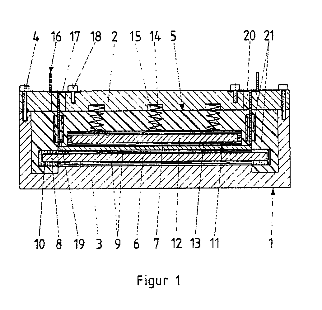
Description
Die Erfindung betrifft einen elektrischen Leistungswiderstand mit einem plattenförmigen, elektrisch isolierenden Trägerkörper, der auf seiner Unterseite eine elektrisch leitende Schicht aufweist, und einem ebenflächigen Widerstandselement, das auf der Oberseite des Trägerkörpers angeordnet ist, wobei ein umlaufender Randbereich des Trägerkörpers vom Widerstandselement unbedeckt ist.The invention relates to an electrical power resistor with a plate-shaped, electrically insulating carrier body, which has an electrically conductive layer on its underside, and a flat resistance element, which is arranged on the top of the carrier body, wherein a peripheral edge region of the carrier body is uncovered by the resistance element.
Ein solcher Leistungswiderstand ist aus der DE-OS 37 15 860 bekannt. Bei diesem elektrischen Leistungswiderstand ist die Unterseite des Trägerkörpers mit einer elektrisch leitenden Farbe beschichtet, die Füllstoffe, wie Kohlenstoff oder Silber, enthält. Auf der Oberseite des Trägerkörpers ist das Widerstandselement in Form einer Folie, einer Dünnschicht oder einer Dickschicht aufgebracht. Das Widerstandselement und der Trägerkörper sind im wesentlichen innerhalb eines Gehäuses angeordnet, das ein elektrisch nichtleitendes Oberteil und ein elektrisch leitendes Unterteil aufweist, das mittels durch den Trägerkörper hindurchgehender Schrauben mit dem Oberteil fest verbunden ist, wobei der Trägerkörper zwischen das Oberteil und das Unterteil des Gehäuses eingespannt ist. Das Oberteil des Gehäuses liegt unmittelbar auf dem unbeschichteten Randbereich des Trägerkörpers auf, während die elektrisch leitende Schicht an der Unterseite des Trägerkörpers mit der Oberfläche des Gehäuseunterteils in Kontakt ist. Ein oberhalb des Trägerkörpers und des Widerstandselements gebildeter Hohlraum in dem Gehäuse ist mit einer elektrisch isolierenden Vergußmasse teilweise gefüllt, die mit dem unbeschichteten Randbereich des Trägerkörpers in Kontakt ist. Die Oberfläche des Trägerkörpers ist somit nur teilweise beschichtet, und die unbeschichtete Oberfläche des Trägerkörpers steht in Kontakt mit der Vergußmasse, dem Oberteil des Gehäuses, der Luft an der Außenseite des Gehäuse und mit den Schrauben, die das Oberteil mit dem Unterteil des Gehäuses verbinden. Dadurch können unerwünschte Teilentladungen an diesen Kontaktstellen entstehen. Auch die auf die Unterseite des Trägerkörpers aufgebrachte elektrisch leitende Farbe kann Teilentladungen nicht verhindern. Der vorbekannte elektrische Leistungswiderstand weist daher Teilentladungsaussetzspannungen von 1 kV bis 2 kV für Teilentladungen < 5 pC auf. Auch hat der vorbekannte Leistungswiderstand nur eine geringe Flächenbelastbarkeit von ca. 10 bis 15 Watt/cm².Such a power resistor is known from DE-OS 37 15 860. In this electrical power resistor, the underside of the carrier body is coated with an electrically conductive paint that contains fillers such as carbon or silver. The resistance element in the form of a film, a thin layer or a thick layer is applied to the top of the carrier body. The resistance element and the carrier body are arranged essentially within a housing which is an electrically non-conductive Has upper part and an electrically conductive lower part which is fixedly connected to the upper part by means of screws passing through the carrier body, the carrier body being clamped between the upper part and the lower part of the housing. The upper part of the housing lies directly on the uncoated edge region of the carrier body, while the electrically conductive layer on the underside of the carrier body is in contact with the surface of the lower housing part. A cavity formed above the carrier body and the resistance element in the housing is partially filled with an electrically insulating casting compound which is in contact with the uncoated edge region of the carrier body. The surface of the carrier body is thus only partially coated, and the uncoated surface of the carrier body is in contact with the sealing compound, the upper part of the housing, the air on the outside of the housing and with the screws which connect the upper part to the lower part of the housing. This can result in undesired partial discharges at these contact points. The electrically conductive paint applied to the underside of the carrier body cannot prevent partial discharges. The known electrical power resistor therefore has partial discharge exposure voltages of 1 kV to 2 kV for partial discharges <5 pC. The previously known power resistor also has a low surface load capacity of approximately 10 to 15 watts / cm².
Ein elektrischer Leistungswiderstand der eingangs beschriebenen Art ist auch aus der DE-OS 38 14 987 bekannt. Bei diesem Leistungswiderstand besteht der Trägerkörper aus mindestens zwei übereinander angeordneten Isolierlagen, zwischen denen ein flächiges Temperaturausgleichselement aus einem wärmeleitenden Material vorgesehen ist, wobei das Temperaturausgleichselement und die zugehörigen Isolierlagen aneinandergrenzen. Das Temperaturausgleichselement ist kleiner als die Isolierlagen, wodurch sich freiliegende Oberflächenabschnitte der Isolierlagen ergeben. Eine Vergußmasse steht ebenfalls in direktem Kontakt mit den freiliegenden Oberflächenabschnitten der Isolierlagen. Das Widerstandselement kann in Form einer Dickschicht aus Cermet auf der Oberseite der obersten Isolierlage des Trägerkörpers aufgebracht sein. Auch bei diesem elektrischen Leistungswiderstand sind die Teilentladungsaussetzspannungen gering und liegen ebenfalls in einem Bereich von 1kV bis 2 kV für Teilentladungen < 5 pC. Ferner hat dieser elektrische Leistungswiderstand auch noch eine geringe Flächenbelastbarkeit von etwa 25 Watt/cm².An electrical power resistor of the type described above is also known from DE-OS 38 14 987. With this power resistor, the carrier body consists of at least two insulating layers arranged one above the other, between which a flat temperature compensation element made of a heat-conducting material is provided, the temperature compensation element and the associated insulation layers adjoining one another. The temperature compensation element is smaller than the insulating layers, which results in exposed surface sections of the insulating layers. A potting compound is also in direct contact with the exposed surface sections of the insulation layers. The resistance element can be applied in the form of a thick layer of cermet on the upper side of the uppermost insulating layer of the carrier body. With this electrical power resistor, too, the partial discharge exposure voltages are low and are also in a range from 1 kV to 2 kV for partial discharges <5 pC. Furthermore, this electrical power resistor also has a low surface load capacity of approximately 25 watts / cm².
Die Aufgabe der Erfindung besteht darin, den gattungsgemäßen elektrischen Leistungswiderstand so auszubilden, daß er bei einer Flächenbelastbarkeit, die höher als die der vorbekannten Leistungswiderstände ist, teilentladungsfrei ist, wobei Teilentladungsfreiheit bei Teilentladungsaussetzspannungen von > 5 kV für Teilentladungen < 5 pC gegeben ist.The object of the invention is to design the generic electrical power resistor so that it is partially discharge-free with a surface load capacity that is higher than that of the known power resistors, with partial discharge freedom at partial discharge suspension voltages of> 5 kV for partial discharges <5 pC.
Die Aufgabe der Erfindung wird dadurch gelöst, daß bei einem gattungsgemäßen elektrischen Leistungswiderstand der Trägerkörper rundum mehrere, einen geschlossenen Überzug bildende, in ihren elektrischen Leiteigenschaften unterschiedliche Schichten aufweist, von denen wenigstens die auf der Oberseite des Trägerkörpers angeordnete, elektrisch leitende Schicht aus Cermet besteht und die den Randbereich des Trägerkörpers bedeckende Schicht aus einem elektrisch isolierenden Material besteht.The object of the invention is achieved in that with a generic electrical power resistance, the carrier body has all around several, forming a closed coating, different in their electrical conductivity properties, of which at least the electrically conductive layer arranged on the top of the carrier body consists of cermet and the layer covering the edge region of the carrier body consists of an electrically insulating material.
Der erfindungsgemäße Leistungswiderstand weist eine hohe Flächenbelastbarkeit von ca. 50 Watt/cm² bei Teilentladungsaussetzspannungen von > 5 kV für Teilentladungen < 5 pC auf. Seine zulässige Dauerbetriebsspannung ist größer als 5 kV, da keine zerstörend wirkende Teilentladungen auftreten.The power resistor according to the invention has a high surface load capacity of approximately 50 watts / cm² with partial discharge exposure voltages of> 5 kV for partial discharges <5 pC. Its permissible continuous operating voltage is greater than 5 kV because there are no destructive partial discharges.
Vorteilhafte Weiterbildungen der Erfindung sind Gegenstand der Unteransprüche 2 bis 18.Advantageous developments of the invention are the subject of
Verschiedene Ausführungsbeispiele der Erfindung sind in den Zeichnungen dargestellt und werden im folgenden näher beschrieben. Es zeigt:
- Figur 1
- einen Schnitt durch einen elektrischen Leistungswiderstand gemäß einem ersten Ausführungsbeispiel der Erfindung,
Figur 2- einen Schnitt durch einen elektrischen Leistungswiderstand gemäß einem zweiten Ausführungsbeispiel der Erfindung,
Figur 3- einen Schnitt durch einen elektrischen Leistungswiderstand gemäß einem dritten Ausführungsbeispiel der Erfindung und
Figur 4- einen Schnitt durch einen elektrischen Leistungswiderstand gemäß einem vierten Ausführungsbeispiel der Erfindung.
- Figure 1
- 3 shows a section through an electrical power resistor according to a first exemplary embodiment of the invention,
- Figure 2
- 3 shows a section through an electrical power resistor according to a second exemplary embodiment of the invention,
- Figure 3
- a section through an electrical power resistor according to a third embodiment of the invention and
- Figure 4
- a section through an electrical power resistor according to a fourth embodiment of the invention.
In den Zeichnungen sind die gleichen oder sich entsprechenden Teile der dargestellten elektrischen Leistungswiderstände mit den gleichen Bezugsziffern bezeichnet.In the drawings, the same or corresponding parts of the electrical power resistors shown are identified by the same reference numerals.
Der in Figur 1 dargestellte elektrische Leistungswiderstand weist ein Gehäuse 1 auf, das aus einem Oberteil 2 und einem Unterteil 3 besteht, das mit dem Oberteil 2 mittels Schrauben 4 oder anderer mechanischer Befestigungselemente, wie Nieten, verbunden ist, die durch das Oberteil 2 und das Unterteil 3 außerhalb eines in dem Gehäuse 1 gebildeten Innenraumes 5 verlaufen. Das Gehäuseunterteil 3 ist gut wärmeleitend und besteht aus einem Metall oder einer Metallegierung, wie z.B. Aluminium, Kupfer, Messing oder ähnlichen Werkstoffen. Das Gehäuseoberteil 2 besteht aus einem elektrisch isolierenden Material, wodurch es potentialfrei ist. Das Gehäuseoberteil kann z.B. aus den folgenden Materialien hergestellt sein: glasierte Keramik, kriechstromfeste Thermo- und Duroplaste, die TE-frei sind (TE ist die Abkürzung für Teilentladung), z.B. Polyamid verstärkt, Polycarbonat, Melaminharz verstärkt, Epoxidharz verstärkt, Polyphenylensulfid oder -oxid.The electrical power resistor shown in Figure 1 has a housing 1, which consists of an
Im Innenraum 5 des Gehäuses 1 sind ein plattenförmiger, elektrisch isolierender Trägerkörper 6 aus einem keramischen Material, wie z.B. Aluminiumoxid, Berylliumoxid, Aluminiumnitrid, und ein Widerstandselement 7 vorgesehen, das auf der Oberseite des Trägerkörpers 6 angeordnet ist. Ein umlaufender Randbereich 8 des Trägerkörpers 6 ist von dem Widerstandselement 7 unbedeckt.In the
Das Widerstandselement 7 besteht bei dem in Figur 1 dargestellten Ausführungsbeispiel der Erfindung aus einer Metallfolie, die aus einem mäanderförmigen Band gebildet ist.In the exemplary embodiment of the invention shown in FIG. 1, the
Der Trägerkörper 6 weist auf seiner Oberseite und seiner Unterseite jeweils eine Schicht 9 aus Cermet auf. Die Cermetschichten 9 sind elektrisch leitend und haben einen im Bereich von 1 kΩ bis 50 MΩ liegenden Widerstand. Die Oberfläche der Cermetschichten 9 sind sehr glatt, d.h. wesentlich glatter als die Oberfläche des unbeschichteten Trägerkörpers 6. Die Cermetschichten 9 sind ferner gasdicht, und es gibt keine Hohlräume in den Cermetschichten 9 oder zwischen den Cermetschichten 9 und dem Trägerkörper 6.The
Die Cermetschichten 9 werden dadurch hergestellt, daß das Cermet in Form einer Paste im Siebdruckverfahren auf den Trägerkörper 6 aufgebracht und nach dem Trocknen gebrannt wird. Die Cermetpaste enthält Edelmetalle bzw. deren Oxide, so z.B. Ruthenium, und ist im Handel als Widerstandspaste z.B. von der Firma Du Pont unter der Bezeichnung "HS80" erhältlich.The
Der umlaufende Randbereich 8 des Trägerkörpers 6 wird von den Cermetschichten 9 nicht bedeckt. Der Randbereich 8 des Trägerkörpers 6 ist aber mit einer elektrisch isolierenden Glasur 10 beschichtet, die einen spezifischen Widerstand > 10⁵ Ωm hat. Die Glasur 10 hat ebenfalls eine sehr glatte Oberfläche, ist gasdicht, hat keine Hohlräume und ist mit dem Trägerkörper 6 hohlraumfrei verbunden. Die Glasur 10 schließt sich ohne Unterbrechung an die Cermetschichten 9 an, so daß die Glasur 10 zusammen mit den Cermetschichten 9 einen geschlossenen, rundum verlaufenden Überzug für den Trägerkörper 6 bilden.The
Die untere Cermetschicht 9 ist in Kontakt mit dem Gehäuseunterteil 3, während die obere Cermetschicht 9 mit dem Widerstandselement 7 in Kontakt ist. Über dem Widerstandselement 7 befindet sich eine Druckverteilungsplatte 11, die kleiner als der Trägerkörper 6 ist und einen Grundkörper 12 aus einem keramischen Material, wie z.B. Aluminiumoxid, aufweist, der rundum mit einer Schicht 13 aus Cermet beschichtet ist.The
Mehrere, voneinander beabstandete Druckfedern 14 sind über der Oberfläche der Druckverteilungsplatte 11 verteilt. Mit ihren oberen Enden stützen sich die Druckfedern 14 an dem Gehäuseoberteil 2 ab, und mit ihren unteren Enden beaufschlagen sie die Oberseite der Druckverteilungsplatte 11, so daß die Druckverteilungsplatte 11 gegen das Widerstandselement 7 und infolgedessen das Widerstandselement 7 gegen die obere Cermetschicht 9 des Trägerkörpers 6 gedrückt wird. Die oberen Enden der Druckfedern 14 sind in Vertiefungen 15 angeordnet, die im Gehäuseoberteil 2 geformt sind, so daß die Federn 14 gegen seitliches Verrutschen gesichert sind.A plurality of spaced apart
An der Oberseite des Gehäuseoberteiles 2 sind zwei Anschlußstücke 16 für den elektrischen Außenanschluß des Leistungswiderstandes befestigt. Die Anschlußstücke 16 bestehen jeweils aus einem winkelförmigen Körper, der einen parallel zu der Oberseite des Gehäuseoberteiles 2 verlaufenden Schenkel 17 aufweist, der in einer Vertiefung in dem Gehäuseoberteil 2 angeordnet und mittels einer Schraube 18 oder einem anderen mechanischen Befestigungselement, wie z.B. einem Niet, an dem Gehäuseoberteil 2 befestigt ist. Durch die Anordnung des Schenkels 17 des Anschlußstücks 16 in einer Vertiefung in dem Gehäuseoberteil 2 kann das Anschlußstück 16 nicht um die Achse der Schraube 18 verdreht werden. Die Anschlußstücke 16 sind durch elektrische Leitungen 19, die durch jeweils eine Bohrung in dem Gehäuseoberteil 2 geführt sind, mit dem Widerstandselement 7 verbunden. Zug- und Druckkräfte, die an den Anschlußstücken 16 eventuell angreifen, werden von den Anschlußstücken 16 nur auf das Gehäuseoberteil 2 und nicht auf die elektrischen Leitungen 19 übertragen.At the top of the
Die Leitungen 19 sind jeweils mit einem isolierenden Silikonschlauch 20 ummantelt, wobei sich zwischen jeder Leitung 19 und dem zugehörigen Silikonschlauch 20 ein Ringraum befindet, der mit einer Vergußmasse 21 gefüllt ist.The
Auch der Innenraum 5 des Gehäuses 1 ist mit der Vergußmasse 21 gefüllt, so daß alle in dem Innenraum 5 befindlichen Bauteile des Widerstandes von der Vergußmasse 21 umschlossen sind. Lediglich zwischen der unteren Cermetschicht 9 und dem Gehäuseunterteil 3 und in den Vertiefungen 15 befindet sich keine Vergußmasse 21.The
Die Vergußmasse 21 besteht aus einer lösungsmittelfreien, füllstofffreien, additionsvernetzenden Zweikomponenten-Silikonkautschukmasse vom RTV-Typ. Sie weist eine hohe Temperaturstabilität >250°C, eine hohe Isolationsfestigkeit ≧ 25 kV/mm, eine sehr gute Wärmeleitfähigkeit von 0,2 Watt/mK und eine extrem gute Benetzbarkeit und Haftfestigkeit an den angrenzenden Oberflächen auf. Die Vergußmasse 21 ist bis zur Durchschlagsspannung absolut TE-frei.The potting
Der in Figur 2 dargestellte elektrische Leistungswiderstand gemäß einem zweiten Ausführungsbeispiel der Erfindung unterscheidet sich von dem in Figur 1 dargestellten Leistungswiderstand nur dadurch, daß anstelle der Druckverteilungsplatte 11 und der Federn 14 ein elastisch verformbares Druckkissen 22 aus einem Silikonkautschuk vorgesehen ist. Das Druckkissen 22 wird durch das Gehäuseoberteil 2 elastisch zusammengedrückt, wobei es sich mit seiner oberen Oberfläche an dem Gehäuseoberteil 2 abstützt und mit seiner unteren Oberfläche das Widerstandselement 7 beaufschlagt, das infolgedessen gegen die obere Cermetschicht 9 des Trägerkörpers 6 gedrückt wird. Der Silikonkautschuk des Druckkissens 22 hat eine definierte Leitfähigkeit mit einem spezifischen Widerstand, der im Bereich > 10³ Ωm < 10⁷ Ωm liegt.The electrical power resistor shown in Figure 2 according to a second embodiment of the invention differs from the power resistor shown in Figure 1 only in that instead of the
Der in Figur 3 dargestellte elektrische Leistungswiderstand gemäß einem dritten Ausführungsbeispiel stimmt mit dem in Figur 1 dargestellten elektrischen Leistungswiderstand darin überein, daß das Widerstandselement 7 zwischen dem plattenförmigen Trägerkörper 6, der auf seiner Oberseite und seiner Unterseite eine Cermetschicht 9 trägt und einen mit einer Glasur 10 beschichteten Randbereich 8 hat, un der Druckverteilungsplatte 11 angeordnet ist, die aus einem keramischen Grundkörper 12 besteht, der rundum mit einer Cermetschicht 13 versehen ist.The electrical power resistance shown in FIG. 3 in accordance with a third exemplary embodiment corresponds to the electrical power resistance shown in FIG. 1 in that the
Im Unterschied zu dem in Figur 1 dargestellten Leistungswiderstand werden bei dem in Figur 3 dargestellten Leistungswiderstand die Druckverteilungsplatte 11 und der plattenförmige Trägerkörper 6 durch ein elastisch verformbares Druckübertragungskissen 25 aus leitfähigem Silikonkautschuk berührungsfrei auf Abstand gehalten. Das Druckübertragungskissen 25 liegt mit seiner oberen Oberfläche an der unteren Oberfläche der Cermetschicht 13 der Druckverteilungsplatte 11 an und beaufschlagt mit seiner unteren Oberfläche das Widerstandselement 7, so daß das Widerstandselement 7 gegen die obere Cermetschicht 9 auf den Trägerkörper 6 gedrückt wird.In contrast to the power resistor shown in FIG. 1, in the power resistor shown in FIG. 3, the
Der Druckaufbau erfolgt durch Federn 14, die über der Druckverteilungsplatte 11 im Abstand voneinander angeordnet sind. Mit ihrem unteren Ende beaufschlagen sie die obere Oberfläche der Cermetschicht 13 der Druckverteilungsplatte und mit ihren oberen Enden stützen sie sich an dem Gehäuseoberteil 2 ab.The pressure is built up by
Der in Figur 4 dargestellte elektrische Leistungswiderstand gemäß einem vierten Ausführungsbeispiel der Erfindung unterscheidet sich von den in den Figuren 1, 2 und 3 dargestellten elektrischen Leistungswiderständen insbesondere dadurch, daß kein separates an die obere Cermetschicht 9 auf dem Trägerkörper 6 angepreßtes Widerstandselement verwendet wird, sondern das Widerstandselement die auf die Oberseite des Trägerkörpers 6 aufgebrachte Cermetschicht 9 selbst ist. Die Cermetschicht 9 stellt somit einen Dickschichtwiderstand dar. An den sich gegenüberliegenden Enden der als Widerstandselement dienenden Cermetschicht 9 befinden sich zwei Anschlußbeschichtungen 23 auf der Oberseite des Trägerkörpers 6, wobei diese Anschlußbeschichtungen 23 beispielsweise aus einer Legierung aus Ag und Pd bestehen. Mit diesen Anschlußbeschichtungen 23 sind die elektrischen Leitungen 19 verlötet. Auf der Unterseite des Trägerkörpers 6 ist keine Cermetschicht sondern eine Metallegierungsschicht 24, z.B. Ag/Pd, vorgesehen, die mit dem Gehäuseunterteil 3 verlötet ist.The electrical power resistor shown in FIG. 4 according to a fourth exemplary embodiment of the invention differs from the electrical power resistors shown in FIGS. 1, 2 and 3 in particular in that no separate resistance element pressed onto the
Bei allen vier Varianten des elektrischen Leistungswiderstandes ist der Randbereich 8 des Trägerkörpers 6 mit einer Glasur beschichtet. Anstelle dieser Glasurschicht kann auch eine Beschichtung mit einem geeigneten Haftvermittler für die Vergußmasse vorgesehen sein.In all four variants of the electrical power resistance, the
Die erfindungsgemäßen elektrischen Leistungswiderstände können für Hochspannungsübertragungsanlagen, Monoverter, Drehstromfrequenzumrichter, Dämpfungswiderstände für Tyristoren usw. verwendet werden, wobei Teilentladungsfreiheit besonders erwünscht ist.The electrical power resistors according to the invention can be used for high-voltage transmission systems, mono switches, three-phase frequency converters, damping resistors for tyristors, etc., freedom from partial discharges being particularly desirable.
Claims (17)
Applications Claiming Priority (2)
| Application Number | Priority Date | Filing Date | Title |
|---|---|---|---|
| DE4014104 | 1990-05-02 | ||
| DE4014104A DE4014104A1 (en) | 1990-05-02 | 1990-05-02 | ELECTRICAL POWER RESISTANCE |
Publications (2)
| Publication Number | Publication Date |
|---|---|
| EP0454904A2 true EP0454904A2 (en) | 1991-11-06 |
| EP0454904A3 EP0454904A3 (en) | 1993-01-13 |
Family
ID=6405589
Family Applications (1)
| Application Number | Title | Priority Date | Filing Date |
|---|---|---|---|
| EP19900125298 Ceased EP0454904A3 (en) | 1990-05-02 | 1990-12-21 | Electrical power resistance |
Country Status (3)
| Country | Link |
|---|---|
| US (1) | US5208576A (en) |
| EP (1) | EP0454904A3 (en) |
| DE (1) | DE4014104A1 (en) |
Cited By (4)
| Publication number | Priority date | Publication date | Assignee | Title |
|---|---|---|---|---|
| EP0637826A1 (en) * | 1993-08-05 | 1995-02-08 | Mcb Industrie | Power resistor, with device for application under pressure on a heat sink |
| EP2592633A1 (en) * | 2011-11-14 | 2013-05-15 | Cressall Resistors Limited | Liquid-cooled resistor device |
| EP3404674A1 (en) * | 2017-05-16 | 2018-11-21 | EBG Elektronische Bauelemente GmbH | Power resistor |
| WO2019105736A1 (en) * | 2017-11-30 | 2019-06-06 | Siemens Aktiengesellschaft | Electrical braking resistor device |
Families Citing this family (5)
| Publication number | Priority date | Publication date | Assignee | Title |
|---|---|---|---|---|
| DE4441280C2 (en) * | 1994-11-19 | 1998-08-27 | Asea Brown Boveri | PTC thermistor and device for current limitation with at least one PTC thermistor |
| US5999083A (en) * | 1999-04-26 | 1999-12-07 | Cts Corporation | Resistive controller using magnetic repulsion |
| DE102004025082B4 (en) * | 2004-05-21 | 2006-12-28 | Infineon Technologies Ag | Electrically and by radiation ignitable thyristor and method for its contacting |
| DE102004062183B3 (en) * | 2004-12-23 | 2006-06-08 | eupec Europäische Gesellschaft für Leistungshalbleiter mbH | Thyristor arrangement, has external resistance and temperature zone each comprising temperature coefficients, where coefficients of external resistance are smaller than coefficients of resistance zone in specific temperature range |
| CN107195405A (en) * | 2017-05-27 | 2017-09-22 | 广东福德电子有限公司 | A kind of thick film plane Power Resistor |
Family Cites Families (5)
| Publication number | Priority date | Publication date | Assignee | Title |
|---|---|---|---|---|
| US4152689A (en) * | 1978-02-13 | 1979-05-01 | American Components Inc. | Electrical resistor package which remains unaffected by ambient stresses and humidity |
| US4419564A (en) * | 1981-03-30 | 1983-12-06 | Texas Instruments Incorporated | Self-regulating electric heater for use in an early fuel evaporation system |
| DE3204683A1 (en) * | 1982-02-11 | 1983-08-18 | Brown, Boveri & Cie Ag, 6800 Mannheim | Device for cooling electrical or electronic components which produce lost heat |
| US4716396A (en) * | 1986-07-10 | 1987-12-29 | Dale Electronics, Inc. | High power density, low corona resistor |
| DE3814987A1 (en) * | 1988-05-03 | 1989-11-16 | Draloric Electronic | ELECTRICAL POWER RESISTANCE |
-
1990
- 1990-05-02 DE DE4014104A patent/DE4014104A1/en active Granted
- 1990-12-21 EP EP19900125298 patent/EP0454904A3/en not_active Ceased
-
1991
- 1991-05-01 US US07/694,118 patent/US5208576A/en not_active Expired - Fee Related
Cited By (7)
| Publication number | Priority date | Publication date | Assignee | Title |
|---|---|---|---|---|
| EP0637826A1 (en) * | 1993-08-05 | 1995-02-08 | Mcb Industrie | Power resistor, with device for application under pressure on a heat sink |
| FR2708782A1 (en) * | 1993-08-05 | 1995-02-10 | Mcb Ind | Resistive power component, with pressure application device on a heat sink. |
| EP2592633A1 (en) * | 2011-11-14 | 2013-05-15 | Cressall Resistors Limited | Liquid-cooled resistor device |
| US8643464B2 (en) | 2011-11-14 | 2014-02-04 | Cressall Resistors Limited | Liquid-cooled resistor device |
| EP3404674A1 (en) * | 2017-05-16 | 2018-11-21 | EBG Elektronische Bauelemente GmbH | Power resistor |
| WO2018210889A1 (en) * | 2017-05-16 | 2018-11-22 | Ebg Elektronische Bauelemente Gmbh | Power resistor |
| WO2019105736A1 (en) * | 2017-11-30 | 2019-06-06 | Siemens Aktiengesellschaft | Electrical braking resistor device |
Also Published As
| Publication number | Publication date |
|---|---|
| DE4014104A1 (en) | 1991-11-14 |
| DE4014104C2 (en) | 1993-04-08 |
| EP0454904A3 (en) | 1993-01-13 |
| US5208576A (en) | 1993-05-04 |
Similar Documents
| Publication | Publication Date | Title |
|---|---|---|
| DE2557598C2 (en) | Shielded coaxial connector for coupling two coaxial cables | |
| EP1502310A2 (en) | Piezoactuator and method for the production thereof | |
| DE4014104C2 (en) | ||
| DE3928036C2 (en) | ||
| EP2104941B1 (en) | Electric component and external contact of an electric component | |
| DE3005773C2 (en) | Surface acoustic wave component | |
| EP0169356B1 (en) | Semiconductor switching device resistant to load varation | |
| EP1537610B1 (en) | Piezoelectric actuator | |
| DE2004776A1 (en) | Semiconductor component | |
| EP0651603A2 (en) | Flexible heat transfer device | |
| DE3116589C2 (en) | Heating device for the plug of an electric cigarette lighter | |
| EP0829897B1 (en) | Electric fuse | |
| DE19711533C2 (en) | PCB arrangement with heat exchanger | |
| DE102022128014A1 (en) | Contact assembly for an electrical connector with a heat capacity element arranged on a contact element | |
| DE3123036A1 (en) | SEMICONDUCTOR MODULE | |
| DE102022207399B4 (en) | Electrically insulating bushing | |
| EP1543534A1 (en) | Electrical component and an assembly comprising said component | |
| DE69716398T2 (en) | High energy and / or power dissolving resistance and manufacturing process | |
| DE19634495C2 (en) | Process for the metallization of component bodies of electro-ceramic components | |
| EP0357977B1 (en) | Soldering device with at least one stirrup electrode heated by electric thermal resistance | |
| BE1030984B1 (en) | Contact assembly for an electrical connector with a heat capacity element arranged on a contact element | |
| DE3232404A1 (en) | Ceramic PTC thermistor having metal plates and power supply leads connected thereto by means of a clamping contact | |
| DE19946199B4 (en) | Electrical component with variable electrical resistance | |
| DE102024118186A1 (en) | Resistance and operating procedures for it | |
| DE102018206966A1 (en) | Sensor element with through-hole |
Legal Events
| Date | Code | Title | Description |
|---|---|---|---|
| PUAI | Public reference made under article 153(3) epc to a published international application that has entered the european phase |
Free format text: ORIGINAL CODE: 0009012 |
|
| AK | Designated contracting states |
Kind code of ref document: A2 Designated state(s): AT BE CH DE DK ES FR GB GR IT LI LU NL SE |
|
| PUAL | Search report despatched |
Free format text: ORIGINAL CODE: 0009013 |
|
| AK | Designated contracting states |
Kind code of ref document: A3 Designated state(s): AT BE CH DE DK ES FR GB GR IT LI LU NL SE |
|
| 17P | Request for examination filed |
Effective date: 19930504 |
|
| 17Q | First examination report despatched |
Effective date: 19940119 |
|
| STAA | Information on the status of an ep patent application or granted ep patent |
Free format text: STATUS: THE APPLICATION HAS BEEN REFUSED |
|
| 18R | Application refused |
Effective date: 19950217 |