EP0455335B1 - Circuit d'interface pour ligne d'abonné - Google Patents
Circuit d'interface pour ligne d'abonné Download PDFInfo
- Publication number
- EP0455335B1 EP0455335B1 EP91302251A EP91302251A EP0455335B1 EP 0455335 B1 EP0455335 B1 EP 0455335B1 EP 91302251 A EP91302251 A EP 91302251A EP 91302251 A EP91302251 A EP 91302251A EP 0455335 B1 EP0455335 B1 EP 0455335B1
- Authority
- EP
- European Patent Office
- Prior art keywords
- voltage
- bias voltage
- analog
- interface circuit
- direct current
- Prior art date
- Legal status (The legal status is an assumption and is not a legal conclusion. Google has not performed a legal analysis and makes no representation as to the accuracy of the status listed.)
- Expired - Lifetime
Links
- 239000003990 capacitor Substances 0.000 description 11
- 238000010586 diagram Methods 0.000 description 4
Images

Classifications
-
- H—ELECTRICITY
- H04—ELECTRIC COMMUNICATION TECHNIQUE
- H04M—TELEPHONIC COMMUNICATION
- H04M3/00—Automatic or semi-automatic exchanges
- H04M3/005—Interface circuits for subscriber lines
-
- H—ELECTRICITY
- H04—ELECTRIC COMMUNICATION TECHNIQUE
- H04M—TELEPHONIC COMMUNICATION
- H04M19/00—Current supply arrangements for telephone systems
- H04M19/001—Current supply source at the exchanger providing current to substations
- H04M19/005—Feeding arrangements without the use of line transformers
Definitions
- the present invention relates to a subscriber line interface circuit and, in particular, to a subscriber line interface circuit having an interfacing capability between analog and digital circuits.
- Such a subscriber line interface circuit has been heretofore connected between an analog telephone terminal and a digital switching system and comprises an interface circuit and an encoding and decoding circuit.
- Fig. 1 is a block diagram of a subscriber line interface circuit showing such a prior art.
- the prior art subscriber line interface circuit comprises an interface circuit 1A and an encoding and decoding 2A (hereinafter referred to as CODEC) having a single power source as shown in Fig. 1.
- CODEC encoding and decoding 2A
- an analog output A O of the CODEC 2A is connected with an input terminal RX of four-wires 4W (hereinafter referred to as four-wire side input terminal) of the interface circuit 1A via a capacitor C2.
- a resistor R4 is connected between the RX terminal and the ground (GND).
- An analog input A I of the CODEC 2A is connected with an output terminal TX (hereinafter referred to as four-wire side output terminal) via a capacitor C1.
- a resistor R3 is connected between the terminal A I and a reference voltage output terminal (V RO ).
- the prior art subscriber line interface circuit has a disadvantage that the frequency characteristics becomes worse since the interface circuit is usually coupled with the CODEC via capacitors in such a manner.
- a high capacity capacitor cannot be built-in an LSI and should be externally added. Therefore, there is a disadvantage that the line circuit on which the capacitors are mounted is cumbersome and expensive.
- a subscriber line interface circuit coupled between a Telephone unit Terminal and a switching system is also known from document: INTERNATIONAL SWITCHING SYMPOSIUM, Paris, 7th-11th May 1979, pages 913-920, S. USUDA et al.: "The BORSHT in digital local switching system".
- the present invention provides a subscriber line interface circuit coupled between a telephone unit terminal and a switching system, comprising a coding and decoding circuit for controlling analog inputted and outputted voltages with a direct current bias voltage and the interface circuit including means for detecting said analog output, means for detecting a direct current bias voltage of said analog output, substracting means for determining the difference between said detected analog outputted voltage and said detected direct current bias voltage and means for driving the telephone unit terminal on the two-wire side, the analog voltage and the direct current bias voltage output terminals of said encoding and decoding circuit being directly connected with the input terminal of said analog outputted voltage detecting means and the direct current bias voltage input terminal of said interface circuit, respectively whereby only desired alternating current signal is outputted to the telephone unit terminal on the two-wire side.
- Fig. 1 is a block diagram of a prior art subscriber line interface circuit.
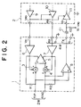
- Fig. 2 is a block diagram showing a first embodiment of a subscriber line interface circuit of the present invention.
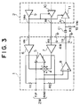
- Fig. 3 is a block diagram showing a second embodiment of a subscriber line interface circuit of the present invention.
- FIG. 2 there is shown a first embodiment of a subscriber line interface circuit of the present invention.
- the subscriber's circuit of the present embodiment is connected between telephone unit terminals (not shown) coupled with terminals TIP and RING and a switching system (not shown) and comprises an interface circuit 1 and an encoding and decoding circuit (CODEC) 2.
- CODEC encoding and decoding circuit
- the interface circuit 1 comprises a voltage detecting amplifier 7 serving as means for detecting an analog output A O from the CODEC 2 via a terminals RX of input and output terminals 4W; a voltage detecting amplifier 6 serving as means for detecting a d.c. bias voltage (V RO ) of an analog output A O via a d.c. bias voltage output terminal V RI from a d.c.
- V RO d.c. bias voltage
- bias voltage output terminals of the CODEC 2 adders 3 and 4 connected with terminal TIP and RING for adding outputs of the voltage detecting amplifiers 6 and 7 to signals from the terminals TIP and RING, respectively; a balanced amplifier 5 connected with the outputs of the adders 3 and 4 which serves as subtracting means for determining the difference between the detected analog output A O and the detected direct current bias voltage V RO , a differential amplifier 8 connected with the terminals TIP and RING for determining the difference between the signals thereon; and resistors R1 and R2 each having one and connected with the output of the balanced amplifier 5 and the terminal TIP or RING, which serves as means for driving the telephone unit terminals on the two-wire side by the output thereof.
- the CODEC 2 has buffer amplifiers 9 - 11, and, out of these amplifiers, the amplifiers 10, 11 receive d.c. bias voltage output from the buffer amplifier 9 as the reference voltages for making amplifying operations.
- the analog output terminal A O and the d.c. bias voltage output terminal V RO of the CODEC 2 are directly connected with the input terminal RX for detecting the analog output and the d.c. bias voltage input terminal V RI of the interface circuit 1, respectively so that only a desired a.c. signal is outputted to the telephone terminal on the two-wire side.
- the outputs of the balanced amplifier 5 in the interface circuit 1 are connected with the two-wire side terminals TIP and RING via resistor R1 and R2. Feedback is applied from the terminals TIP and RING to the input of the balanced amplifier 5 so that desired impedances are obtained based on these resistors R1 and R2. That is, a signal is inputted to the adder 3 from the terminal TIP and the output of the adder 3 is inputted to one of the differential inputs (positive side) of the balanced amplifier 5. A signal is inputted to the adder 4 from the terminal RING and the output of the adder 4 is inputted to one of the differential inputs (negative side) of the balanced amplifiers 5.
- the terminal RX of the four-wire side input terminals in the interface circuit 1 is connected with the input of the voltage detecting amplifier 7 so that the output thereof is supplied to the other input of the afore-mentioned adder 4.
- an output terminal V RO having a reference voltage V REF which is a d.c. bias voltage of the analog output A O of the CODEC 2 is connected with the voltage detecting amplifier 6 for detecting the d.c. bias voltage, the output of which is connected with the other input of the adder 3 in the interface circuit 1.
- subtracting operation is performed by an application of opposite polarity inputs to the balanced amplifier 5 in the afore-mentioned operation. This makes it possible to eliminate the influence of the d.c. bias voltage to the power supply of the two-wire side.
- FIG. 3 there is showing a second embodiment of a subscriber line interface circuit of the present invention.
- the present embodiment is identical with the above-mentioned first embodiment except that the output of the voltage detecting amplifier 6 for detecting the d.c. bias voltage is reversed and then coupled to another input of the adder 4, which performs a subtracting operation of a d.c. bias voltage from an analog output signal including the d.c. bias voltage of the CODEC 2.
- addition of the analog output signal to an inverted signal of the d.c. bias voltage is equivalent to subtraction of a signal of a d.c. bias voltage from an analog output signal.
- the subscriber line interface circuit of the present invention includes an interface circuit comprising means having a voltage detecting amplifier and the like for detecting a d.c. bias voltage of an analog output and subtracting means for determining the difference between the analog output and said detected d.c. bias voltage so that an analog output terminal of the CODEC can be directly connected with an RX input terminal of the interface circuit.
- the present invention can improve the frequency characteristics of the subscriber line interface circuit. Since the present invention can eliminate some of external capacitors, the compact and inexpensive subscriber's circuit can be realized. Since the d.c. bias voltage of the CODEC provides a bias voltage for means for detecting an analog output as well as an output idling current in accordance with the present invention, the output of the analog output detecting means may not be of bipolar type. Since noised generated in the d.c. bias voltage of the CODEC is cancelled by the subtraction operation in accordance with the present invention, the noise is reduced.
Landscapes
- Engineering & Computer Science (AREA)
- Signal Processing (AREA)
- Power Engineering (AREA)
- Interface Circuits In Exchanges (AREA)
Claims (4)
- Circuit d'interface de ligne d'abonné (1, 2) couplé entre un terminal téléphonique et un système de commutation, comprenant un circuit de codage et de décodage (2) pour commander les tensions entrées et sorties analogiques (AI, AO) avec une tension de polarisation à courant continu (VRO) et le circuit d'interface (1) comportant un moyen (7) pour détecter ladite sortie analogique, un moyen (6) pour détecter une tension de polarisation à courant continu (VRO) de ladite tension de sortie analogique (AO), un moyen de soustraction (3, 4, 5) pour déterminer la différence entre ladite tension sortie analogique détectée (AO) et ladite tension de polarisation détectée à courant continu (VRO) et un moyen (R1, R2) pour attaquer le terminal téléphonique sur le côté deux fils, les bornes de sortie de tension analogique et de tension de polarisation à courant continu dudit circuit de codage et de décodage (2) étant directement connectées à la borne d'entrée (RX) dudit moyen de détection de tension de sortie analogique (7) et à la borne d'entrée de tension de polarisation à courant continu (VRI) dudit circuit d'interface (1), respectivement, d'où il résulte que seul le signal à courant alternatif désiré est sorti vers le terminal téléphonique sur le côté deux fils.
- Circuit d'interface de ligne d'abonné selon la revendication 1, dans lequel ledit moyen de soustraction comprend un amplificateur équilibré (5).
- Circuit d'interface de ligne d'abonné selon la revendication 1, dans lequel ledit moyen (6) pour détecter la tension de polarisation à courant continu (VRO) comprend un amplificateur de détection de tension (6).
- Circuit d'interface de ligne d'abonné (1, 2) couplé entre un terminal téléphonique et un système de commutation, comprenant un circuit de codage et de décodage (2) pour commander les tensions entrées et sorties analogiques (AI, AO) avec une tension de polarisation à courant continu (VRO) et le circuit d'interface (1) comportant un moyen (7) pour détecter ladite tension de sortie analogique, un moyen (6) pour détecter une tension de polarisation à courant continu (VRO) de ladite tension de sortie analogique (AO), au moins un moyen (4) pour individuellement ou directement additionner la sortie dudit moyen (7) pour détecter la tension de sortie analogique à la sortie dudit moyen (6) pour détecter la tension de polarisation à courant continu de la tension de sortie analogique, un moyen de soustraction (5) pour déterminer la différence entre la tension sortie analogique (AO) et la tension de polarisation à courant continu (VRO) qui sont obtenues par au moins un desdits moyens d'addition, et un moyen (R1, R2) pour attaquer le terminal téléphonique sur le côté deux fils, les bornes de sortie de tension analogique et de tension de polarisation à courant continu (AO, VRO) dudit circuit de codage et de décodage (2) étant directement connectées à la borne d'entrée (VRI) dudit moyen de détection de tension de sortie analogique (7) et à la borne d'entrée de tension de polarisation à courant continu (VRI) dudit circuit d'interface (1), respectivement, d'où il résulte que seul le signal de courant alternatif désiré est sorti vers le terminal téléphonique sur le côté deux fils.
Applications Claiming Priority (2)
| Application Number | Priority Date | Filing Date | Title |
|---|---|---|---|
| JP66525/90 | 1990-03-16 | ||
| JP2066525A JP2687656B2 (ja) | 1990-03-16 | 1990-03-16 | 加入者線回路 |
Publications (2)
| Publication Number | Publication Date |
|---|---|
| EP0455335A1 EP0455335A1 (fr) | 1991-11-06 |
| EP0455335B1 true EP0455335B1 (fr) | 1994-10-12 |
Family
ID=13318379
Family Applications (1)
| Application Number | Title | Priority Date | Filing Date |
|---|---|---|---|
| EP91302251A Expired - Lifetime EP0455335B1 (fr) | 1990-03-16 | 1991-03-15 | Circuit d'interface pour ligne d'abonné |
Country Status (4)
| Country | Link |
|---|---|
| US (1) | US5422948A (fr) |
| EP (1) | EP0455335B1 (fr) |
| JP (1) | JP2687656B2 (fr) |
| DE (1) | DE69104538T2 (fr) |
Families Citing this family (2)
| Publication number | Priority date | Publication date | Assignee | Title |
|---|---|---|---|---|
| US5598467A (en) * | 1994-12-09 | 1997-01-28 | National Semiconductor Corporation | Signal interface circuit with selectable signal interface parameters |
| FR2848680B1 (fr) * | 2002-12-16 | 2005-04-01 | Teem Photonics | Reseau a gaine artificielle en optique integree presentant une variation de couplage ainsi que son procede de realisation |
Family Cites Families (4)
| Publication number | Priority date | Publication date | Assignee | Title |
|---|---|---|---|---|
| US4682356A (en) * | 1980-04-04 | 1987-07-21 | Siemens Corporation | Apparatus for transmitting and/or receiving balanced signals on a two-wire telecommunication line |
| US4896351A (en) * | 1985-06-27 | 1990-01-23 | Siemens Ag | Apparatus for separating dc current and ac current components of a composite signal |
| US4953206A (en) * | 1986-11-17 | 1990-08-28 | At&T Bell Laboratories | Methods of and apparatus for providing substantially error-free transmitted data |
| CA1257027A (fr) * | 1987-03-10 | 1989-07-04 | Rolf Meier | Circuit de compensation pour amplificateur integrateur |
-
1990
- 1990-03-16 JP JP2066525A patent/JP2687656B2/ja not_active Expired - Lifetime
-
1991
- 1991-03-15 EP EP91302251A patent/EP0455335B1/fr not_active Expired - Lifetime
- 1991-03-15 DE DE69104538T patent/DE69104538T2/de not_active Expired - Lifetime
-
1994
- 1994-09-12 US US08/304,598 patent/US5422948A/en not_active Expired - Lifetime
Also Published As
| Publication number | Publication date |
|---|---|
| JPH03267898A (ja) | 1991-11-28 |
| US5422948A (en) | 1995-06-06 |
| EP0455335A1 (fr) | 1991-11-06 |
| DE69104538D1 (de) | 1994-11-17 |
| JP2687656B2 (ja) | 1997-12-08 |
| DE69104538T2 (de) | 1995-05-04 |
Similar Documents
| Publication | Publication Date | Title |
|---|---|---|
| US4697152A (en) | Fully differential switched capacitor amplifier having autozeroed common-mode feedback | |
| EP0582862B1 (fr) | Circuit amplificateur à condensateurs commutés | |
| US5491434A (en) | Circuit and method of differential amplitude detection | |
| US4827505A (en) | Subscriber line interface circuit | |
| US5406149A (en) | Noise canceler | |
| JPS63169865A (ja) | 有効インピーダンス・ライン・フイード回路 | |
| US4431874A (en) | Balanced current multiplier circuit for a subscriber loop interface circuit | |
| US4677667A (en) | Subscriber line circuit having improved AC impedance matching | |
| US4701720A (en) | Capacitive feedback to boost amplifier slew rate | |
| US4608464A (en) | Interface circuit interconnecting a bidirectional two-wire line with unidirectional four-wire lines | |
| EP0415080B1 (fr) | Dispositif de conversion de signaux électriques analogiques non symétriques en signaux entièrement différentiels | |
| US4571554A (en) | Balanced amplifier device | |
| US5465064A (en) | Weighted summing circuit | |
| US4088961A (en) | Operational amplifier driver circuit | |
| EP0789477B1 (fr) | Circuit d'interface de ligne d'abonné réalisable par technologie CMOS | |
| EP0455335B1 (fr) | Circuit d'interface pour ligne d'abonné | |
| JPS59185432A (ja) | 光受信回路 | |
| US5335271A (en) | Ring trip detection circuit | |
| US5804978A (en) | Circuit for feeding a Wheatstone Bridge with a rectangular waveform voltage | |
| EP0215677A2 (fr) | Circuit d'interface de ligne d'abonné ayant des moyens pour combiner des signaux de contre-réaction continus et alternatifs | |
| US6963238B2 (en) | Level shift circuit | |
| US5271059A (en) | Method and configuration for forming a line termination of a telephone line | |
| US6950514B2 (en) | Voltage reference filter for subscriber line interface circuit | |
| US4635115A (en) | Synchronous separation circuit | |
| US4412189A (en) | Switchable signal compressor/signal expander |
Legal Events
| Date | Code | Title | Description |
|---|---|---|---|
| PUAI | Public reference made under article 153(3) epc to a published international application that has entered the european phase |
Free format text: ORIGINAL CODE: 0009012 |
|
| 17P | Request for examination filed |
Effective date: 19910323 |
|
| AK | Designated contracting states |
Kind code of ref document: A1 Designated state(s): DE FR GB |
|
| 17Q | First examination report despatched |
Effective date: 19940120 |
|
| GRAA | (expected) grant |
Free format text: ORIGINAL CODE: 0009210 |
|
| AK | Designated contracting states |
Kind code of ref document: B1 Designated state(s): DE FR GB |
|
| REF | Corresponds to: |
Ref document number: 69104538 Country of ref document: DE Date of ref document: 19941117 |
|
| ET | Fr: translation filed | ||
| PLBE | No opposition filed within time limit |
Free format text: ORIGINAL CODE: 0009261 |
|
| STAA | Information on the status of an ep patent application or granted ep patent |
Free format text: STATUS: NO OPPOSITION FILED WITHIN TIME LIMIT |
|
| 26N | No opposition filed | ||
| REG | Reference to a national code |
Ref country code: GB Ref legal event code: IF02 |
|
| REG | Reference to a national code |
Ref country code: GB Ref legal event code: 732E |
|
| REG | Reference to a national code |
Ref country code: FR Ref legal event code: TP |
|
| PGFP | Annual fee paid to national office [announced via postgrant information from national office to epo] |
Ref country code: FR Payment date: 20100324 Year of fee payment: 20 |
|
| PGFP | Annual fee paid to national office [announced via postgrant information from national office to epo] |
Ref country code: GB Payment date: 20100310 Year of fee payment: 20 |
|
| PGFP | Annual fee paid to national office [announced via postgrant information from national office to epo] |
Ref country code: DE Payment date: 20100415 Year of fee payment: 20 |
|
| REG | Reference to a national code |
Ref country code: FR Ref legal event code: CD |
|
| REG | Reference to a national code |
Ref country code: DE Ref legal event code: R071 Ref document number: 69104538 Country of ref document: DE |
|
| REG | Reference to a national code |
Ref country code: GB Ref legal event code: PE20 Expiry date: 20110314 |
|
| PG25 | Lapsed in a contracting state [announced via postgrant information from national office to epo] |
Ref country code: GB Free format text: LAPSE BECAUSE OF EXPIRATION OF PROTECTION Effective date: 20110314 |
|
| PG25 | Lapsed in a contracting state [announced via postgrant information from national office to epo] |
Ref country code: DE Free format text: LAPSE BECAUSE OF EXPIRATION OF PROTECTION Effective date: 20110315 |