EP0455411A1 - Korrelationsdetektor für FM-Signale - Google Patents
Korrelationsdetektor für FM-Signale Download PDFInfo
- Publication number
- EP0455411A1 EP0455411A1 EP91303702A EP91303702A EP0455411A1 EP 0455411 A1 EP0455411 A1 EP 0455411A1 EP 91303702 A EP91303702 A EP 91303702A EP 91303702 A EP91303702 A EP 91303702A EP 0455411 A1 EP0455411 A1 EP 0455411A1
- Authority
- EP
- European Patent Office
- Prior art keywords
- output
- signal
- coupled
- indicating
- filter bank
- Prior art date
- Legal status (The legal status is an assumption and is not a legal conclusion. Google has not performed a legal analysis and makes no representation as to the accuracy of the status listed.)
- Granted
Links
Images

Classifications
-
- G—PHYSICS
- G01—MEASURING; TESTING
- G01S—RADIO DIRECTION-FINDING; RADIO NAVIGATION; DETERMINING DISTANCE OR VELOCITY BY USE OF RADIO WAVES; LOCATING OR PRESENCE-DETECTING BY USE OF THE REFLECTION OR RERADIATION OF RADIO WAVES; ANALOGOUS ARRANGEMENTS USING OTHER WAVES
- G01S7/00—Details of systems according to groups G01S13/00, G01S15/00, G01S17/00
- G01S7/02—Details of systems according to groups G01S13/00, G01S15/00, G01S17/00 of systems according to group G01S13/00
- G01S7/021—Auxiliary means for detecting or identifying radar signals or the like, e.g. radar jamming signals
Definitions
- This application relates generally to detecting frequency modulated (FM) signals and more particularly to detecting signals from FM altimeters and radars.
- FM frequency modulated
- FM signals are well suited for measuring the distance from a transmitter to an object from which the FM signal reflects. Signals in which the frequency increases or decreases linearly ("chirped signals") are particularly well suited for these functions. For this reason, FM signals are sometimes used in altimeters on aircraft. Also, FM signals are used in radars which are often on aircraft or other moving bodies.
- FM signals emitted by altimeters or radars on aircraft can indicate the presence of the aircraft.
- FM altimeter or FM radar signals are used to detect aircraft. These signals are generally very directive and are not always directed at the device trying to detect the aircraft. For example, an altimeter signal is transmitted directly at the ground below the aircraft. A device trying to detect the aircraft would receive only the side lobes of the Fm signal. Thus, the received FM signal would be at a relatively low level.
- Existing systems use what is called a "walk-through receiver" to detect FM signals.
- the walk-through receiver contains a relatively narrow bandpass filter. As the FM signal changes in frequency, its frequency will, for some period of time, fall in the passband of the filter.
- the output of the filter will be a pulse having a non-zero value when the FM signal has a frequency in the passband of the filter.
- Ordinary pulse detection techniques are applied to the output of the filter to detect the pulses which signify the presence of an FM signal.
- the walk-through receiver has a drawback in that only a portion of the energy in the FM signal appears in the output pulse. In effect, the signal level is attenuated. This attenuation reduces the sensitivity of the receiver and makes detection of an FM signal less likely.
- the foregoing and other objects are accomplished in a receiver where the received signal is split into two channels.
- the first channel contains a delay element. Both channels are fed to a phase detector, the output of which is fed to a filter bank.
- the outputs of all the filters in the filter bank are fed to a logic circuit which selects the filter output with the largest signal level and passes that output to a threshold circuit. If the signal level exceeds a predetermined threshold, the threshold circuit signals the detection of an FM signal.
- FIG. 1 shows a block diagram of a receiver fabricated according to the invention
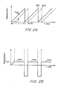
- FIG. 2A shows a frequency versus time plot of the inputs to the phase detector of the circuit in FIG. 1
- FIG. 2B shows a frequency versus time plot of the output of the phase detector in FIG. 1.
- FIG. 1 shows a block diagram of a receiver 10 designed to detect the presence of an aircraft 12.
- Aircraft 12 contains a radio altimeter (not shown) which operates by transmitting a signal 16A towards the ground 14.
- Signal 16A reflects from the ground and the altimeter determines the height of aircraft 12 above ground 14 by measuring the back and forth propagation delay of signal 16A.
- receiver 10 detects the presence of aircraft 10 by detecting the presence of a chirped signal.
- signal 16A is directed from aircraft 12 to ground 14.
- Signal 16A is not necessarily received by receiver 10.
- the altimeter (not shown) on aircraft 12 invariably transmits sidelobe signals such as signals 16b and 16c. At least a portion of sidelobe signals 16b and 16c will be received by receiver 10 when aircraft 12 is sufficiently close to receiver 10. Thus, receiver 10 will most likely detect the sidelobe signals 16b or 16c.
- antenna 18 is some antenna of known construction.
- antenna 18 has a beam pattern with broad angular coverage.
- the received signal is amplified by amplifier 20.
- Amplifier 20 is of known construction.
- the amplified signal is split into two paths. One path runs directly to input 21a of phase detector 24. The second path runs to input 21b of phase detector 24 through delay element 22.
- Delay element 22 is any substantially non-dispersive delay element of known construction. Delay element 22 delays the signal by an amount T d .
- FIG. 2A shows a received waveform 202.
- Waveform 202 sweeps from a frequency f min to f max in T seconds. These frequency sweeps are repeated at regular intervals.
- the type of signal received will dictate the numeric values of the parameters of signal 202.
- the operating characteristics of the circuit elements in FIG. 1 are selected accordingly. For example, if T had a value of 10ms and the difference between f max and f min were 100MHz, a value of 60ns would be an appropriate value of T d . In general T d is selected to be approximately as given by Eq. 1:
- Signal 202 is applied to input 21a of phase detector 24.
- Signal 204 is a replica of signal 202, but delayed by an amount T d .
- Signal 204 is fed to input 21b of phase detector 24.
- Phase detector 24 is a phase detector of known construction. Phase detector 24 may also be thought of as a mixer. The output of phase detector 24 is a signal with a frequency equal to the difference between the signals at inputs 21a and 21b.
- FIG. 2B shows the output of phase detector 24 for input signals 202 and 204.
- the major portion of the output of phase detector 24 consists of segments 250a, 250b, 250c... which are of constant frequency f DIF .
- filter bank 26 is here an FFT processor and an analog to digital converter of known construction. The filtering properties of FFT processors are well known. However, other techniques for fabricating filter bank 26 could be employed.
- Filter bank 26 has a plurality of outputs. Each output represents the cumulative strength of signals in a particular frequency band averaged over some time window (called the "integration time of the FFT").
- the signal of FIG. 2B will produce an output in the band containing the frequency f DIF .
- the output signal from phase detector 24 will also produce signals on outputs of filter bank 26 corresponding to other frequency bands. However, these other signals will be at a lower average level because the signal of FIG. 2B has those frequencies for much shorter periods of time.
- filter bank 26 The outputs of filter bank 26 are fed to logic circuit 28 which selects the output with the largest magnitude.
- logic circuit 28 can be constructed using conventional digital logic circuit design techniques.
- the output of logic circuit 28 indicates the level of the largest output of filter bank 26. This level is provided to threshold circuit 30. If the level of the largest signal exceeds a predetermined threshold, threshold circuit 30 produces an output indicating a chirped signal has been detected. This output may be used by some utilization device (not shown) which may interpret the output as indicating the presence of an aircraft.
- the threshold used by threshold circuit 30 could be set adaptively. In other words, the threshold could be increased if many RF signals and noise are detected. Conversely, if the RF environment is relatively free of noise and other signals, the threshold can be lowered.
- logic circuit 28 could be modified to sequentially pass to threshold circuit 30 several of the largest signals from filter bank 26. If several aircraft are present, several signals might exceed the threshold set by threshold circuit 30 and the OUTPUT could indicate the presence of several aircraft.
- signal 202 of FIG. 2A produces a signal out of phase detector 24 with mainly a frequency f DIF .
- f DIF is the increase in frequency of signal 202 in time T d .
- the value of f DIF thus depends on how fast the frequency of signal 202 is changing (sometimes called the "chirp slope").
- Certain radio altimeters or FM radios will use different chirp slopes and thus produce different values of f DIF . By determining in which frequency band the largest signal falls, the chirp slope of the signal can be determined.
- Knowing the chirp slope of the signal which produced an OUTPUT signal may allow some utilization device to identify the source of the chirped signal.
- logic circuit 28 could be modified so that the largest signal was selected from one of a few selected frequency bands corresponding to chirp slopes of interest.
Landscapes
- Engineering & Computer Science (AREA)
- Radar, Positioning & Navigation (AREA)
- Remote Sensing (AREA)
- Computer Networks & Wireless Communication (AREA)
- Physics & Mathematics (AREA)
- General Physics & Mathematics (AREA)
- Radar Systems Or Details Thereof (AREA)
Applications Claiming Priority (2)
| Application Number | Priority Date | Filing Date | Title |
|---|---|---|---|
| US51650190A | 1990-04-30 | 1990-04-30 | |
| US516501 | 1990-04-30 |
Publications (2)
| Publication Number | Publication Date |
|---|---|
| EP0455411A1 true EP0455411A1 (de) | 1991-11-06 |
| EP0455411B1 EP0455411B1 (de) | 1995-12-13 |
Family
ID=24055880
Family Applications (1)
| Application Number | Title | Priority Date | Filing Date |
|---|---|---|---|
| EP19910303702 Expired - Lifetime EP0455411B1 (de) | 1990-04-30 | 1991-04-24 | Korrelationsdetektor für FM-Signale |
Country Status (3)
| Country | Link |
|---|---|
| EP (1) | EP0455411B1 (de) |
| JP (1) | JPH04230884A (de) |
| DE (1) | DE69115343T2 (de) |
Citations (3)
| Publication number | Priority date | Publication date | Assignee | Title |
|---|---|---|---|---|
| US4298985A (en) * | 1979-12-31 | 1981-11-03 | The United States Of America As Represented By The Secretary Of The Army | Digital filter bank detector |
| US4800388A (en) * | 1985-02-06 | 1989-01-24 | Tokyo Keiki Company, Ltd. | Apparatus for measuring pulse compression ratio |
| US4860013A (en) * | 1988-04-04 | 1989-08-22 | The United States Of America As Represented By The Secretary Of The Navy | Automatic thresholding multichannel digital radar early warning system |
-
1991
- 1991-04-24 DE DE1991615343 patent/DE69115343T2/de not_active Expired - Fee Related
- 1991-04-24 EP EP19910303702 patent/EP0455411B1/de not_active Expired - Lifetime
- 1991-04-30 JP JP9887791A patent/JPH04230884A/ja active Pending
Patent Citations (3)
| Publication number | Priority date | Publication date | Assignee | Title |
|---|---|---|---|---|
| US4298985A (en) * | 1979-12-31 | 1981-11-03 | The United States Of America As Represented By The Secretary Of The Army | Digital filter bank detector |
| US4800388A (en) * | 1985-02-06 | 1989-01-24 | Tokyo Keiki Company, Ltd. | Apparatus for measuring pulse compression ratio |
| US4860013A (en) * | 1988-04-04 | 1989-08-22 | The United States Of America As Represented By The Secretary Of The Navy | Automatic thresholding multichannel digital radar early warning system |
Non-Patent Citations (1)
| Title |
|---|
| SOVIET INVENTIONS ILLUSTRATED week 8623, 20 June 1986, abstract no. 148706 W/01, Derwent Publications Ltd., London, GB; & SU - A - 1188901 (DANIELYAN S A) 30.10.1985 * |
Also Published As
| Publication number | Publication date |
|---|---|
| DE69115343T2 (de) | 1996-06-27 |
| EP0455411B1 (de) | 1995-12-13 |
| JPH04230884A (ja) | 1992-08-19 |
| DE69115343D1 (de) | 1996-01-25 |
Similar Documents
| Publication | Publication Date | Title |
|---|---|---|
| US10078128B2 (en) | Digital receiver techniques in radar detectors | |
| US6211812B1 (en) | Quiet radar method and apparatus | |
| EP1502126B1 (de) | Verfahren und vorrichtung zur radarimpulsdetektion und -schätzung in der physischen schicht eines drahtlosen lan | |
| US7683827B2 (en) | System and method for reducing the effect of a radar interference signal | |
| US7403153B2 (en) | System and method for reducing a radar interference signal | |
| CA1341358C (en) | Continuous wave radar altimeter | |
| US4067013A (en) | Automatic thresholding and reference circuit | |
| US10288726B2 (en) | Impulse noise detection and removal for radar and communication systems | |
| EP1933164B1 (de) | Radargerät und verfahren zur inter-radarortseinstellung | |
| US6087976A (en) | Radar object detection system having normalized range sensitivity | |
| US4546356A (en) | Process for the protection of a radar against jamming and radar for putting this process into effect | |
| EP0408112A1 (de) | Pulsradargerät und für den Einbau in dieses Gerät geeignete Pulsdiskriminierungsschaltung | |
| US6977611B1 (en) | FM-CW altimeter detector | |
| US8780955B2 (en) | Signal processing apparatus, radar apparatus, and signal processing method | |
| US7064703B2 (en) | Methods and apparatus for randomly modulating radar altimeters | |
| US5081461A (en) | Correlation detector for FM signals | |
| US4121212A (en) | Double sideband pulse radar | |
| EP0455411A1 (de) | Korrelationsdetektor für FM-Signale | |
| JP2000321351A (ja) | 目標検出方法及びレーダ装置 | |
| EP4040181A1 (de) | Radarsignalverarbeitungsvorrichtung, radarvorrichtung, radarsignalverarbeitungsverfahren und radarsignalverarbeitungsprogramm | |
| RU2792418C1 (ru) | Многоканальное устройство обработки фазоманипулированных радиолокационных сигналов | |
| KR102362586B1 (ko) | 레이더 간섭에 대한 증가된 강건성을 위한 수신기 아키텍처 | |
| EP0045773A1 (de) | Empfängeranordnung zum unterdrücken von durch frequenzmodulierte störsender ausgestrahlten störsignalen | |
| EP4152042A1 (de) | Verfahren zur verarbeitung von radarsignalen und radarvorrichtung | |
| Steen | Spectral Energy Requirements and Adjacent-Channel Crosstalk in CAS |
Legal Events
| Date | Code | Title | Description |
|---|---|---|---|
| PUAI | Public reference made under article 153(3) epc to a published international application that has entered the european phase |
Free format text: ORIGINAL CODE: 0009012 |
|
| AK | Designated contracting states |
Kind code of ref document: A1 Designated state(s): DE FR GB |
|
| 17P | Request for examination filed |
Effective date: 19920501 |
|
| 17Q | First examination report despatched |
Effective date: 19940125 |
|
| GRAA | (expected) grant |
Free format text: ORIGINAL CODE: 0009210 |
|
| AK | Designated contracting states |
Kind code of ref document: B1 Designated state(s): DE FR GB |
|
| REF | Corresponds to: |
Ref document number: 69115343 Country of ref document: DE Date of ref document: 19960125 |
|
| ET | Fr: translation filed | ||
| PLBE | No opposition filed within time limit |
Free format text: ORIGINAL CODE: 0009261 |
|
| STAA | Information on the status of an ep patent application or granted ep patent |
Free format text: STATUS: NO OPPOSITION FILED WITHIN TIME LIMIT |
|
| 26N | No opposition filed | ||
| PGFP | Annual fee paid to national office [announced via postgrant information from national office to epo] |
Ref country code: FR Payment date: 19970318 Year of fee payment: 7 |
|
| PGFP | Annual fee paid to national office [announced via postgrant information from national office to epo] |
Ref country code: DE Payment date: 19970324 Year of fee payment: 7 |
|
| PGFP | Annual fee paid to national office [announced via postgrant information from national office to epo] |
Ref country code: GB Payment date: 19970326 Year of fee payment: 7 |
|
| PG25 | Lapsed in a contracting state [announced via postgrant information from national office to epo] |
Ref country code: GB Free format text: LAPSE BECAUSE OF NON-PAYMENT OF DUE FEES Effective date: 19980424 |
|
| PG25 | Lapsed in a contracting state [announced via postgrant information from national office to epo] |
Ref country code: FR Free format text: THE PATENT HAS BEEN ANNULLED BY A DECISION OF A NATIONAL AUTHORITY Effective date: 19980430 |
|
| GBPC | Gb: european patent ceased through non-payment of renewal fee |
Effective date: 19980424 |
|
| PG25 | Lapsed in a contracting state [announced via postgrant information from national office to epo] |
Ref country code: DE Free format text: LAPSE BECAUSE OF NON-PAYMENT OF DUE FEES Effective date: 19990202 |
|
| REG | Reference to a national code |
Ref country code: FR Ref legal event code: ST |