EP0455839A1 - Circuit de mesure de la puissance réelle et réactive pour un convertisseur avec la tension continue appliquée - Google Patents
Circuit de mesure de la puissance réelle et réactive pour un convertisseur avec la tension continue appliquée Download PDFInfo
- Publication number
- EP0455839A1 EP0455839A1 EP90106585A EP90106585A EP0455839A1 EP 0455839 A1 EP0455839 A1 EP 0455839A1 EP 90106585 A EP90106585 A EP 90106585A EP 90106585 A EP90106585 A EP 90106585A EP 0455839 A1 EP0455839 A1 EP 0455839A1
- Authority
- EP
- European Patent Office
- Prior art keywords
- reactive power
- inverter
- transistor
- phase
- output
- Prior art date
- Legal status (The legal status is an assumption and is not a legal conclusion. Google has not performed a legal analysis and makes no representation as to the accuracy of the status listed.)
- Granted
Links
- 238000001514 detection method Methods 0.000 claims abstract description 22
- 238000005259 measurement Methods 0.000 claims abstract description 11
- 230000003321 amplification Effects 0.000 claims description 11
- 238000003199 nucleic acid amplification method Methods 0.000 claims description 11
- 238000012545 processing Methods 0.000 description 3
- 230000001105 regulatory effect Effects 0.000 description 3
- 238000011161 development Methods 0.000 description 2
- 230000006870 function Effects 0.000 description 2
- 238000000034 method Methods 0.000 description 2
- 229920006395 saturated elastomer Polymers 0.000 description 2
- 238000012935 Averaging Methods 0.000 description 1
- 239000003990 capacitor Substances 0.000 description 1
- 238000006243 chemical reaction Methods 0.000 description 1
- 230000001276 controlling effect Effects 0.000 description 1
- 238000009499 grossing Methods 0.000 description 1
- 230000036039 immunity Effects 0.000 description 1
- 238000002955 isolation Methods 0.000 description 1
- 230000001960 triggered effect Effects 0.000 description 1
Images


Classifications
-
- G—PHYSICS
- G01—MEASURING; TESTING
- G01R—MEASURING ELECTRIC VARIABLES; MEASURING MAGNETIC VARIABLES
- G01R21/00—Arrangements for measuring electric power or power factor
- G01R21/001—Measuring real or reactive component; Measuring apparent energy
Definitions
- the invention relates to a device for detecting active and / or reactive power on a phase of an inverter, wherein a measurement signal corresponding to the phase current for detecting the active power directly or for detecting the reactive power after phase rotation by ⁇ / 2 can be actuated with a control signal Switch is turned on, the active or reactive power corresponds to a smoothed output signal of a superposition element.
- Such a device is known from DE 35 04 623 A1.
- the switch to which a measurement signal corresponding to the phase current is supplied, is actuated with the switching signal which determines the switching state of the inverter switch operating on this phase.
- the switches are controlled with the control signals of the inverter, which are generated by means of a tax rate.
- the inverter usually feeds a three-phase motor.
- the active and reactive power supplied to it and therefore also the measured active and reactive power signals are low when idling or at low converter output frequencies.
- the active power supplied to an engine is idling only a few percent of the value at the nominal operating point.
- the measured power signals are to be processed digitally after an analog-to-digital conversion and the analog-to-digital converter used has only a limited resolution, the accuracy achieved will in many cases not be sufficient for meaningful further processing of the measured values.
- the converter-fed motor can temporarily be loaded up to twice the nominal power, the standardization of the analog-digital converter must be carried out in such a way that no overflow occurs at twice the nominal power. As a result, however, the active and / or reactive power signals cannot be correctly converted into digital values at a low converter output frequency, which can be processed in a microprocessor of a controller.
- the invention is based on the object of specifying a device for detecting active and / or reactive power in an inverter with an impressed intermediate circuit voltage, in which a measurement error due to dead times of the control circuit and switching times of the inverter valves is avoided.
- the amplification of the superposition elements of the device for detecting active and / or reactive powers can be switched in stages, the switching depending on the output signal of the superposition element being controlled by means of a comparator with hysteresis in such a way that an upper switching threshold of the hysteresis is exceeded
- the microprocessor controls the switching of the amplification of the superimposed elements with the aid of a clock-controlled memory cell, the output signal of the comparator being fed to the microprocessor and the clock-controlled memory cell.
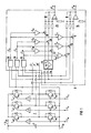
- FIG. 1 shows a pulse-controlled inverter 2 with a device 4 for detecting active and / or reactive power P W and / or P B.
- the pulse inverter 2 is electrically connected in parallel to a voltage intermediate circuit 6.
- This voltage intermediate circuit 6 and the pulse inverter 2 are components of a converter, not shown.
- each output U, V and W is alternating with the positive or negative voltage rail + U ZK or -U ZK of the voltage intermediate circuit via a converter valve T U1 , T U2 , T V1 , T V2 , T W1 and T W2 6 connectable, the intermediate circuit voltage supplied by a line converter is kept constant via the capacitor.
- the control signals for the converter valves T U1 to T W2 are denoted by S U , S v and S W.
- the individual transistors free-wheeling diodes are electrically connected in parallel. Further obvious details (driver stages, means for electrical isolation, tax rate, etc.) are not shown in this figure 1 because of the clarity.
- measured values i U , i V and i W for the phase currents are formed at the pulse converter outputs U, V and W. These measured values i U , i V and i W are fed to the device 4 for detecting active and / or reactive power P W and / or P B.
- the respective measured value i U , i V and i W for detecting the active power P W is fed to a switch 8, 10 and 12, each switch 8, 10 and 12 using a switching status signal Z U , Z V and Z W of the converter valve T U1 to T W2 assigned to the corresponding phase U, V and W is actuated.
- the corresponding measured value P W for the entire inverter 2 is formed by adding and averaging the pulse-width-modulated values at the switches 8, 10 and 12 in a superposition element 14 to the resulting active power value P W.
- the value of the instantaneous active power P W which is subject to harmonics, is smoothed by means of the RC circuit of the operational amplifier of the superposition element 14.
- the reactive power P B can be recorded in the same way, it being only necessary to first rotate the measurement signals i U , i V and i W by 90 ° in their phase position by means of a phase rotator 16.
- the measured values which are phase-shifted in this way become corresponding switches 18, 20 and 22, which are also operated with the signals Z U , Z V and Z W which determine the switching state of the converter valves T U1 to T W2 .
- analog switches 8, 10, 12, 18, 20 and 22 instead of the analog overlay elements 14 and 24, corresponding digital modules can be used.
- a detection device 26 or 28 or 30 is provided per phase U or V or W. These detection devices 26, 28 and 30 are all constructed identically, so that in the following only one detection device 26 is mentioned as representative.
- the detection device 26 is linked on the input side to a pulse inverter output U and to the negative voltage rail -U ZK of the voltage intermediate circuit 6.
- the detection device 26 can also be linked on the input side to an output U of the inverter 2 and the positive voltage rail + U ZK of the voltage intermediate circuit 6, an inverter then having to be provided at the output of the detection device 26 when the switching state signal Z U of the device 4 shown to detect the active and / or reactive power P W and / or P B is to be supplied.
- Embodiments of the detection device 26 are shown in more detail in FIGS. 3 to 6.
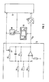
- FIG. 2 shows a device for increasing the accuracy of the device 4 for detecting the active and / or reactive power P W and / or P B.
- the inverter 2 usually feeds a load, in particular a three-phase motor, there is a regulating and control device for regulating and controlling the load, which is advantageously equipped with a microprocessor 32. So that the microprocessor 32 can further process the determined active and / or reactive power measured values P W and / or P B , these values P W and P B must be converted from analog to digital will.
- a commercially available 8-bit analog-digital converter 34 is provided as the analog-digital converter.
- the amplification of the superimposition elements 14 and 24 is designed to be switchable in several stages. For reasons of clarity, only the overlay member 14 of the device 4 is shown in FIG.
- the output signal P W of the superposition element 14 is supplied on the one hand to the analog-digital converter 34 and on the other hand to a comparator 36 with hysteresis.
- the output of the analog-to-digital converter 34 is connected to the microprocessor 32 of a regulating and control device, not shown, and the output of the comparator 36 is connected to an input D of a clock-controlled memory cell 38.
- the output Q of this clock-controlled memory cell 38 (clock-state-controlled D flip-flop) is linked on the one hand to an actuation input of a switch 40 and on the other hand to the microprocessor 32.
- Clock signals T from the microprocessor 32 are supplied to the clock input C of the clock-controlled memory cell 38.
- the switch 40 is electrically connected in series with a resistor 42.
- This series circuit is electrically connected in parallel to the RC circuit of the operational amplifier of the superposition element 14.
- the gain of the superimposition element 14 results from the ratio of the resistor 43 to the resistor 44 or, when the switch 40 is closed, the effective resistance of the parallel connection of the resistors 42 and 43 to the resistor 44.
- Any desired gain can be set in a switchable manner by means of the resistor 42 and a switch , the switchover being controlled as a function of the output signal P W of the superposition element 14 by means of the comparator 36 and the clock-state-controlled D flip-flop 38.
- the analog-to-digital converter 34 can very finely resolve the measurement signal P W , ie the measuring range of the analog-to-digital converter 34 can be fully utilized at each amplification stage.
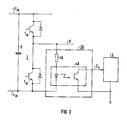
- FIG. 3 shows a first exemplary embodiment of the detection device 26 in detail. Since only one detection device 26 is shown for reasons of equality, only the corresponding phase U is shown by the pulse-controlled inverter 2.
- the detection device 26 consists of a series connection of a resistor 46 (current limiting resistor) and an optocoupler 48, in particular a fast optocoupler.
- the transmitter of the optocoupler 48 is at the potential of the output U of the inverter 2 and the receiver of the optocoupler 48 is at the potential of the device 4.
- the optocoupler 48 is directly connected to a voltage rail + U ZK or -U ZK des Voltage intermediate circuit 6 connected. This will result in a high du / dt load on the Optocoupler 48 avoided.
- FIG. 4 shows a further development of the embodiment of the detection device 26 according to FIG. 3.
- the optocoupler 48 is not switched directly via the output U of the inverter 2, but by means of a transistor circuit 50.
- the optocoupler 48 is fed from an auxiliary voltage source U H.
- the transistor circuit 50 consists, for example, of a small-signal bipolar transistor 52, at the base B of which a voltage divider 54 is connected, which is connected on the one hand to the output U of the inverter 2 and on the other hand to the negative voltage rail -U ZK of the voltage intermediate circuit 6.
- the collector K is electrically conductively connected to the transmitter of the optocoupler 48.
- the transistor 52 Due to the high current amplification in the case of small-signal bipolar transistors, only a small base current is required for the transistor 52, so that only small losses occur in the resistors 56 and 58 of the voltage divider 54. Since the transistor 52 is supplied with very different base currents depending on the intermediate circuit voltage and is therefore highly saturated at least at high intermediate circuit voltages as a result of a higher base current, the transistor 52 can only switch off slowly.
- FIG. 4 A development of the embodiment of the detection device 26 according to FIG. 4 is illustrated in FIG.
- the transistor circuit 50 is expanded by a zener diode 60 and a current source resistor 62.
- the fast zener diode 60 is electrically connected in parallel to the base-emitter path of the transistor 52 and the current source resistor 62 is electrically conductively connected to the emitter E.
- This transistor circuit 50 thus works as a current source that can be switched on and off. As a result, the transistor 52 never operates in the saturated state with a sufficiently small resistor 46 and consequently switches very much quickly.
- a fast Zener diode 62 is a prerequisite for fast switching on and off.
- FIG. 6 shows an alternative embodiment to the embodiment of the detection device 26 according to FIG. 5.
- a voltage source U BE and a decoupling diode 64 are used.
- the equivalent circuit U BE - 64 acts like a fast Zener diode 60 (function of the Zener diode).
- This voltage U BE and the voltage U H can be derived from a control device (not shown) for the lower converter valves T U2 , T V2 and T W2 of the pulse-controlled inverter 2, which means no additional effort.
Landscapes
- Engineering & Computer Science (AREA)
- Power Engineering (AREA)
- Physics & Mathematics (AREA)
- General Physics & Mathematics (AREA)
- Inverter Devices (AREA)
- General Induction Heating (AREA)
- Emergency Protection Circuit Devices (AREA)
- Investigating Or Analysing Biological Materials (AREA)
- Control Of Electrical Variables (AREA)
Priority Applications (4)
| Application Number | Priority Date | Filing Date | Title |
|---|---|---|---|
| DE90106585T DE59004440D1 (de) | 1990-04-06 | 1990-04-06 | Vorrichtung zur Erfassung von Wirk- und/oder Blindleistung bei einem Wechselrichter mit eingeprägter Gleichspannung. |
| AT90106585T ATE100940T1 (de) | 1990-04-06 | 1990-04-06 | Vorrichtung zur erfassung von wirk- und/oder blindleistung bei einem wechselrichter mit eingepraegter gleichspannung. |
| EP90106585A EP0455839B1 (fr) | 1990-04-06 | 1990-04-06 | Circuit de mesure de la puissance réelle et réactive pour un convertisseur avec la tension continue appliquée |
| FI911203A FI911203A7 (fi) | 1990-04-06 | 1991-03-12 | Anordning foer maetning av avgiven effekt och/eller reaktiv effekt vid vaexelriktare anfattande forcerad likstroem. |
Applications Claiming Priority (1)
| Application Number | Priority Date | Filing Date | Title |
|---|---|---|---|
| EP90106585A EP0455839B1 (fr) | 1990-04-06 | 1990-04-06 | Circuit de mesure de la puissance réelle et réactive pour un convertisseur avec la tension continue appliquée |
Publications (2)
| Publication Number | Publication Date |
|---|---|
| EP0455839A1 true EP0455839A1 (fr) | 1991-11-13 |
| EP0455839B1 EP0455839B1 (fr) | 1994-01-26 |
Family
ID=8203864
Family Applications (1)
| Application Number | Title | Priority Date | Filing Date |
|---|---|---|---|
| EP90106585A Expired - Lifetime EP0455839B1 (fr) | 1990-04-06 | 1990-04-06 | Circuit de mesure de la puissance réelle et réactive pour un convertisseur avec la tension continue appliquée |
Country Status (4)
| Country | Link |
|---|---|
| EP (1) | EP0455839B1 (fr) |
| AT (1) | ATE100940T1 (fr) |
| DE (1) | DE59004440D1 (fr) |
| FI (1) | FI911203A7 (fr) |
Cited By (2)
| Publication number | Priority date | Publication date | Assignee | Title |
|---|---|---|---|---|
| WO2008135576A3 (fr) * | 2007-05-08 | 2009-01-22 | Ericsson Telefon Ab L M | Résistances intégrées à commande numérique et procédés |
| CN110023767A (zh) * | 2016-11-29 | 2019-07-16 | 庞巴迪无接触运行有限责任公司 | 确定用于感应式功率传输的系统的转换器的切换电流的方法和装置以及控制方法 |
Citations (2)
| Publication number | Priority date | Publication date | Assignee | Title |
|---|---|---|---|---|
| DE3504623A1 (de) * | 1984-05-04 | 1985-11-07 | Siemens AG, 1000 Berlin und 8000 München | Vorrichtung zur erfassung von wirk- und/oder blindstrom und/oder deren leistung bei einem wechselrichter mit vorgegebener eingangsgleichspannung, insbesondere einem pulswechselrichter |
| DE3625011A1 (de) * | 1985-11-08 | 1987-05-21 | Aeg Elotherm Gmbh | Einrichtung zur messung der wirkleistung in einem als schwingkreis ausgebildeten lastkreis eines statischen elektrischen umrichters |
-
1990
- 1990-04-06 EP EP90106585A patent/EP0455839B1/fr not_active Expired - Lifetime
- 1990-04-06 AT AT90106585T patent/ATE100940T1/de not_active IP Right Cessation
- 1990-04-06 DE DE90106585T patent/DE59004440D1/de not_active Expired - Fee Related
-
1991
- 1991-03-12 FI FI911203A patent/FI911203A7/fi not_active Application Discontinuation
Patent Citations (2)
| Publication number | Priority date | Publication date | Assignee | Title |
|---|---|---|---|---|
| DE3504623A1 (de) * | 1984-05-04 | 1985-11-07 | Siemens AG, 1000 Berlin und 8000 München | Vorrichtung zur erfassung von wirk- und/oder blindstrom und/oder deren leistung bei einem wechselrichter mit vorgegebener eingangsgleichspannung, insbesondere einem pulswechselrichter |
| DE3625011A1 (de) * | 1985-11-08 | 1987-05-21 | Aeg Elotherm Gmbh | Einrichtung zur messung der wirkleistung in einem als schwingkreis ausgebildeten lastkreis eines statischen elektrischen umrichters |
Cited By (5)
| Publication number | Priority date | Publication date | Assignee | Title |
|---|---|---|---|---|
| WO2008135576A3 (fr) * | 2007-05-08 | 2009-01-22 | Ericsson Telefon Ab L M | Résistances intégrées à commande numérique et procédés |
| US7602327B2 (en) | 2007-05-08 | 2009-10-13 | Telefonaktiebolaget Lm Ericsson (Publ) | Digitally controllable on-chip resistors and methods |
| CN101675487B (zh) * | 2007-05-08 | 2012-05-30 | Lm爱立信电话有限公司 | 可数控的片上电阻器及方法 |
| CN110023767A (zh) * | 2016-11-29 | 2019-07-16 | 庞巴迪无接触运行有限责任公司 | 确定用于感应式功率传输的系统的转换器的切换电流的方法和装置以及控制方法 |
| CN110023767B (zh) * | 2016-11-29 | 2021-08-17 | 庞巴迪无接触运行有限责任公司 | 确定用于感应式功率传输的系统的转换器的切换电流的方法和装置以及控制方法 |
Also Published As
| Publication number | Publication date |
|---|---|
| FI911203A0 (fi) | 1991-03-12 |
| DE59004440D1 (de) | 1994-03-10 |
| ATE100940T1 (de) | 1994-02-15 |
| EP0455839B1 (fr) | 1994-01-26 |
| FI911203A7 (fi) | 1991-10-07 |
Similar Documents
| Publication | Publication Date | Title |
|---|---|---|
| DE3131574C2 (de) | "Stromregelschaltung für einen über eine Leistungstreiberstufe gesteuerten Verbraucher" | |
| DE60303981T2 (de) | Fahrzeuglenkungsregelsystem | |
| DE3712185A1 (de) | Laststromerfassungseinrichtung fuer stromrichter mit pulsdauermodulation | |
| DE3844234A1 (de) | Vorrichtung zur stromversorgung einer mehrphasigen belastung und verfahren zum betreiben eines wechselrichters | |
| EP0082392B1 (fr) | Arrangement d'un circuit pour l'enregistrement de la polarité de courant d'une charge d'un hacheur réversible à courant continu | |
| EP0799515A1 (fr) | Circuiterie et procede de fonctionnement d'un mecanisme de commande de reglage | |
| DE112015006875T5 (de) | Leistungswandler | |
| DE102014103374A1 (de) | System und verfahren zum kalibrieren eines netzteils | |
| EP2265964B1 (fr) | Procédé et dispositif de mesure du courant dans des lignes de phase | |
| DE69815971T2 (de) | Schaltnetzteil mit verzögerungs-unempfindlichem taktgeber in der regelschleife | |
| DE3625091A1 (de) | Endstufe in brueckenschaltung | |
| DE102008022497A1 (de) | Laststeuervorrichtung und zugehöriges Verfahren zur Verarbeitung eines Diagnosesignals | |
| DE3437513A1 (de) | Basistreiberschaltung fuer einen leistungstransistor | |
| DE102009022314A1 (de) | Verfahren und Schaltungsanordnung zur Messung des Stroms durch eine induktive Last | |
| EP0455839B1 (fr) | Circuit de mesure de la puissance réelle et réactive pour un convertisseur avec la tension continue appliquée | |
| EP0489971B1 (fr) | Méthode et dispositif pour la commande d'un système onduleur à m-impulsions, comprenant un onduleur "master" et au moins un onduleur "slave" | |
| DE3442607C2 (fr) | ||
| EP1317696A1 (fr) | Dispositif d'activation d'un appareil de commande | |
| DE2511651C3 (de) | Sicherheitsschaltung mit einem Schwellenkreis | |
| EP4555613A1 (fr) | Dispositif de surveillance et procédé de surveillance d'un convertisseur inverse, convertisseur inverse | |
| DE3014658C2 (de) | Schaltungsanordnung zur Ermittlung von Übergängen eines Wechselsignals | |
| DE102016203604A1 (de) | Überwachung einer Spulensteuerung | |
| DE102020102647B4 (de) | Anordnung und Verfahren zur Erzeugung eines Verstärkungssignals für Messverstärker | |
| EP2504917B1 (fr) | Dispositif et procédé pour mesurer un courant de moteur d'un moteur à courant continu | |
| EP0629048A2 (fr) | Agencement de conversion analogique-numérique de signaux de niveaux différents |
Legal Events
| Date | Code | Title | Description |
|---|---|---|---|
| PUAI | Public reference made under article 153(3) epc to a published international application that has entered the european phase |
Free format text: ORIGINAL CODE: 0009012 |
|
| 17P | Request for examination filed |
Effective date: 19901205 |
|
| AK | Designated contracting states |
Kind code of ref document: A1 Designated state(s): AT BE CH DE DK ES FR GB GR IT LI LU NL SE |
|
| RBV | Designated contracting states (corrected) |
Designated state(s): AT CH DE DK ES FR GB IT LI SE |
|
| 17Q | First examination report despatched |
Effective date: 19930701 |
|
| GRAA | (expected) grant |
Free format text: ORIGINAL CODE: 0009210 |
|
| AK | Designated contracting states |
Kind code of ref document: B1 Designated state(s): AT CH DE DK ES FR GB IT LI SE |
|
| PG25 | Lapsed in a contracting state [announced via postgrant information from national office to epo] |
Ref country code: IT Free format text: LAPSE BECAUSE OF FAILURE TO SUBMIT A TRANSLATION OF THE DESCRIPTION OR TO PAY THE FEE WITHIN THE PRESCRIBED TIME-LIMIT;WARNING: LAPSES OF ITALIAN PATENTS WITH EFFECTIVE DATE BEFORE 2007 MAY HAVE OCCURRED AT ANY TIME BEFORE 2007. THE CORRECT EFFECTIVE DATE MAY BE DIFFERENT FROM THE ONE RECORDED. Effective date: 19940126 Ref country code: ES Free format text: THE PATENT HAS BEEN ANNULLED BY A DECISION OF A NATIONAL AUTHORITY Effective date: 19940126 Ref country code: DK Effective date: 19940126 Ref country code: SE Effective date: 19940126 |
|
| REF | Corresponds to: |
Ref document number: 100940 Country of ref document: AT Date of ref document: 19940215 Kind code of ref document: T |
|
| REF | Corresponds to: |
Ref document number: 59004440 Country of ref document: DE Date of ref document: 19940310 |
|
| PG25 | Lapsed in a contracting state [announced via postgrant information from national office to epo] |
Ref country code: AT Effective date: 19940406 |
|
| PG25 | Lapsed in a contracting state [announced via postgrant information from national office to epo] |
Ref country code: CH Effective date: 19940430 Ref country code: LI Effective date: 19940430 |
|
| GBT | Gb: translation of ep patent filed (gb section 77(6)(a)/1977) |
Effective date: 19940407 |
|
| ET | Fr: translation filed | ||
| PLBE | No opposition filed within time limit |
Free format text: ORIGINAL CODE: 0009261 |
|
| STAA | Information on the status of an ep patent application or granted ep patent |
Free format text: STATUS: NO OPPOSITION FILED WITHIN TIME LIMIT |
|
| REG | Reference to a national code |
Ref country code: CH Ref legal event code: PL |
|
| 26N | No opposition filed | ||
| PGFP | Annual fee paid to national office [announced via postgrant information from national office to epo] |
Ref country code: GB Payment date: 19950320 Year of fee payment: 6 |
|
| PGFP | Annual fee paid to national office [announced via postgrant information from national office to epo] |
Ref country code: FR Payment date: 19950426 Year of fee payment: 6 |
|
| PGFP | Annual fee paid to national office [announced via postgrant information from national office to epo] |
Ref country code: DE Payment date: 19950621 Year of fee payment: 6 |
|
| PG25 | Lapsed in a contracting state [announced via postgrant information from national office to epo] |
Ref country code: GB Effective date: 19960406 |
|
| GBPC | Gb: european patent ceased through non-payment of renewal fee |
Effective date: 19960406 |
|
| PG25 | Lapsed in a contracting state [announced via postgrant information from national office to epo] |
Ref country code: FR Effective date: 19961227 |
|
| PG25 | Lapsed in a contracting state [announced via postgrant information from national office to epo] |
Ref country code: DE Effective date: 19970101 |
|
| REG | Reference to a national code |
Ref country code: FR Ref legal event code: ST |