EP0455874B1 - Magnétoscope - Google Patents
Magnétoscope Download PDFInfo
- Publication number
- EP0455874B1 EP0455874B1 EP90124058A EP90124058A EP0455874B1 EP 0455874 B1 EP0455874 B1 EP 0455874B1 EP 90124058 A EP90124058 A EP 90124058A EP 90124058 A EP90124058 A EP 90124058A EP 0455874 B1 EP0455874 B1 EP 0455874B1
- Authority
- EP
- European Patent Office
- Prior art keywords
- write
- signals
- read
- vco
- signal
- Prior art date
- Legal status (The legal status is an assumption and is not a legal conclusion. Google has not performed a legal analysis and makes no representation as to the accuracy of the status listed.)
- Expired - Lifetime
Links
- 238000010586 diagram Methods 0.000 description 2
- 125000000524 functional group Chemical group 0.000 description 2
- 230000010363 phase shift Effects 0.000 description 2
- 238000000034 method Methods 0.000 description 1
- 239000004065 semiconductor Substances 0.000 description 1
Images
Classifications
-
- H—ELECTRICITY
- H04—ELECTRIC COMMUNICATION TECHNIQUE
- H04N—PICTORIAL COMMUNICATION, e.g. TELEVISION
- H04N5/00—Details of television systems
- H04N5/76—Television signal recording
- H04N5/91—Television signal processing therefor
-
- G—PHYSICS
- G11—INFORMATION STORAGE
- G11B—INFORMATION STORAGE BASED ON RELATIVE MOVEMENT BETWEEN RECORD CARRIER AND TRANSDUCER
- G11B27/00—Editing; Indexing; Addressing; Timing or synchronising; Monitoring; Measuring tape travel
- G11B27/02—Editing, e.g. varying the order of information signals recorded on, or reproduced from, record carriers
- G11B27/022—Electronic editing of analogue information signals, e.g. audio or video signals
- G11B27/029—Insert-editing
Definitions
- the invention relates to a video recorder with which it is possible to add further information to information which has already been recorded on a tape. This is usually done in those sections of the recording tracks that are assigned to invisible picture lines of the video signal.
- This invention is based on the knowledge that the interference signals observed in the previous subsequent recording mainly result from the fact that the modulated data write signals are not in phase with the previously read, ie previously recorded, signals when switching from the read to the write mode.
- the demodulator temporarily suspends, which serves to demodulate the read modulated FM signal.
- the VCO which is used for converting the data write signals into FM signals, is kept in phase with the read signals in the reading mode. If a switch is then made to the write operating mode, information is subsequently recorded without a phase jump in relation to the FM signal which has already been recorded. Smaller switching disturbances can occur when switching over, but no more phase jumps.
- the function of a conventional demodulator is not disturbed by the mere switching disturbances. It is therefore possible to start writing information immediately after switching from the reading mode to the writing mode. Due to the undisturbed function of the demodulator, this information can be read from the beginning without errors. This allows the write capacity to be fully used.
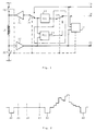
- a first switchover device which includes a gate circuit 17, a data signal switch 18, a read ground switch 19 and a write ground switch 20, implements the switchover from the read mode to the write mode.
- the circuit described so far is identical to conventional circuits. If the data signal switch 18 is continuously held in the position shown in FIG. 1, ie the position in which it supplies data write signals from the data input connection 16 to the VCO 13, the circuit has exactly the function of a conventional circuit. This function is described below.
- the write ground switch 20 is closed and the read ground switch 19 is open.
- the write signal switch 14 which forms a second switching device in connection with the gate circuit 17
- the read ground switch 19 is closed and the write ground switch 20 is open. Read signals are then supplied to an output terminal 21 via the sense amplifier 12.
- FIG. 2 shows the level curve of an already recorded signal over time.
- the levels actually correspond to different wavelengths of an FM signal.
- the signal has a horizontal synchronization pulse 22 at regular time intervals. 64 ⁇ sec each pass from pulse to pulse when recorded in the NTSC standard. No information has yet been recorded between the first two horizontal synchronizing pulses 22 in FIG. 2. This is the section for an invisible line. In contrast, information for a visible line is present between the second and the third pulse.
- Two vertical solid lines in FIG. 2 indicate the time span over which information can subsequently be written into the track section for the invisible line. The associated times are designated in FIG. 2 with Z1 and Z3.
- the write signal switch 14 and the data signal switch 18 are permanently in the positions shown in FIG. 1.
- the two ground switches are switched to switch from the read to the write mode. This switchover generally results in a phase jump in the recorded FM signal.
- the phase difference between the already recorded FM signal and the subsequently recorded signal is not very small, the phase shift leads to the demodulator being interrupted when the signals are read later. Therefore, in the prior art, the procedure is such that the write signal is not immediately included in the subsequent writing Data write signals is modulated, but that this is only started with a delay. This later point in time is designated by Z2 in FIG. 2. It can be seen that a lot of recording capacity is lost because the write signal cannot be immediately started to be modulated with data write signals at the time Z1.
- the problem just mentioned is avoided in the circuit according to FIG. 1 in that it has the functional groups which are outlined in dash-dot lines in FIG. 1. It is a PLL 23 and the data signal switch 18 already mentioned. This is not present in the conventional circuit, since the data write signals are continuously supplied from the data input connection 16 to the VCO 13.
- the PLL 23 compares the phases of the VCO output signal and the read signal from the sense amplifier 12 with one another. The control deviation signal is integrated and this integrated signal is applied to the second switching contact of the data signal switch 18.
- the data write signal from the data input connection 16 is present at the first contact. The result of this arrangement is that when the data signal switch 18 is switched to the PLL output signal, the phase of the VCO output signal continuously coincides with the phase of the read signal.
- the gate circuit 17 now issues the command to switch from the read to the write mode of operation based on the write and read signals supplied to it, not only the two ground switches 19 and 20 are switched, but also the data signal switch 18 is switched, so that the VCO 13 no longer receives the PLL output signal, but the data write signal.
- the frequency-modulated data write signal from the VCO 13 then connects in phase with the previously read signal.
- the switching back and forth between write and read mode can also be carried out with a different circuit structure than that shown in FIG. 1.
- the changeover switches are designed as semiconductor components.
- the only essential for the function of the circuit according to FIG. 1 is that the output signal from the VCO 13 is kept in phase with the read, previously recorded signal by the action of the PLL 23. As a result, the subsequently recorded signal connects in phase with the previously recorded signal.
Landscapes
- Engineering & Computer Science (AREA)
- Multimedia (AREA)
- Signal Processing (AREA)
- Television Signal Processing For Recording (AREA)
- Signal Processing For Digital Recording And Reproducing (AREA)
Claims (1)
- Enregistreur vidéo comprenant- un dispositif d'enregistrement / de lecture (10) pour enregistrer des signaux FM sur une bande et pour lire des signaux FM enregistrés,- un VCO (13),- une borne d'entrée de données (16) pour transmettre des signaux d'enregistrement de données au VCO,- un premier dispositif de commutation (17, 19, 20) pour commuter le dispositif d'enregistrement / de lecture entre un mode d'enregistrement et un mode de lecture,- un deuxième dispositif de commutation (14, 17) pour commuter l'entrée d'enregistrement du dispositif d'enregistrement / de lecture entre des signaux d'enregistrement vidéo (15) à enregistrer et des signaux d'enregistrement de données modulés à enregistrer qui sont produit par le VCO, et- un circuit PLL (23) qui compare entre elles les phases du signal lu en mode de lecture et du signal de sortie du VCO et délivre un signal d'écart de réglage intégré en tant que signal de sortie PLL,
le premier dispositif de commutation (17-20) étant réalisé de sorte qu'il comprend en outre un commutateur de signal de données (18) qui, en mode de lecture, commute le signal de sortie PLL sur l'entrée du VCO,
et qui, en mode d'enregistrement, commute la borne d'entrée de données (16) sur l'entrée du VCO (13).
Applications Claiming Priority (2)
| Application Number | Priority Date | Filing Date | Title |
|---|---|---|---|
| DE4014513A DE4014513A1 (de) | 1990-05-07 | 1990-05-07 | Videorecorder |
| DE4014513 | 1990-05-07 |
Publications (2)
| Publication Number | Publication Date |
|---|---|
| EP0455874A1 EP0455874A1 (fr) | 1991-11-13 |
| EP0455874B1 true EP0455874B1 (fr) | 1995-09-27 |
Family
ID=6405816
Family Applications (1)
| Application Number | Title | Priority Date | Filing Date |
|---|---|---|---|
| EP90124058A Expired - Lifetime EP0455874B1 (fr) | 1990-05-07 | 1990-12-13 | Magnétoscope |
Country Status (4)
| Country | Link |
|---|---|
| US (1) | US5173812A (fr) |
| EP (1) | EP0455874B1 (fr) |
| JP (1) | JP3043460B2 (fr) |
| DE (2) | DE4014513A1 (fr) |
Families Citing this family (3)
| Publication number | Priority date | Publication date | Assignee | Title |
|---|---|---|---|---|
| JPH05166349A (ja) * | 1991-12-13 | 1993-07-02 | Victor Co Of Japan Ltd | 磁気記録再生装置 |
| JP3161479B2 (ja) * | 1992-02-13 | 2001-04-25 | ソニー株式会社 | 情報信号の記録装置 |
| DE4217207C1 (fr) * | 1992-05-23 | 1992-12-17 | Grundig E.M.V. Elektro-Mechanische Versuchsanstalt Max Grundig Hollaend. Stiftung & Co Kg, 8510 Fuerth, De |
Family Cites Families (11)
| Publication number | Priority date | Publication date | Assignee | Title |
|---|---|---|---|---|
| NL277854A (fr) * | 1961-05-01 | |||
| GB1572346A (en) * | 1976-03-19 | 1980-07-30 | Rca Corp | Velocity and phase control for a disc recording and reproducing apparatus |
| US4175267A (en) * | 1976-07-30 | 1979-11-20 | Sony Corporation | Method and apparatus of inserting an address signal in a video signal |
| DE2844897A1 (de) * | 1978-10-14 | 1980-04-17 | Blaupunkt Werke Gmbh | Informationsaufzeichnungs- und informationswiedergabegeraet |
| JPS55114084A (en) * | 1979-02-23 | 1980-09-03 | Hitachi Ltd | Magnetic recording and reproducing device |
| JPS5669981A (en) * | 1979-11-12 | 1981-06-11 | Sony Corp | Phase servo circuit |
| JPS58164383A (ja) * | 1982-03-25 | 1983-09-29 | Sony Corp | ビデオ信号記録装置 |
| DE3315740C2 (de) * | 1983-04-30 | 1985-02-21 | Telefunken Fernseh Und Rundfunk Gmbh, 3000 Hannover | Videorecorder mit Aufzeichnung eines Videotext-Signals |
| US4734792A (en) * | 1984-07-24 | 1988-03-29 | Ricoh Company, Ltd. | Record address data recording apparatus for use with a VTR or the like |
| DE8711830U1 (de) * | 1987-09-01 | 1987-12-10 | Gref, Burkhard, 5411 Simmern | Gerät zum Mischen von Video- und Bildsignalen |
| DE3806330A1 (de) * | 1988-02-27 | 1989-09-07 | Broadcast Television Syst | Verfahren zur umschaltung von wiedergabesignalen in einem videomagnetbandgeraet |
-
1990
- 1990-05-07 DE DE4014513A patent/DE4014513A1/de not_active Withdrawn
- 1990-12-13 EP EP90124058A patent/EP0455874B1/fr not_active Expired - Lifetime
- 1990-12-13 DE DE59009725T patent/DE59009725D1/de not_active Expired - Fee Related
-
1991
- 1991-04-19 US US07/688,633 patent/US5173812A/en not_active Expired - Fee Related
- 1991-05-07 JP JP3101640A patent/JP3043460B2/ja not_active Expired - Lifetime
Also Published As
| Publication number | Publication date |
|---|---|
| JP3043460B2 (ja) | 2000-05-22 |
| JPH04230183A (ja) | 1992-08-19 |
| DE59009725D1 (de) | 1995-11-02 |
| DE4014513A1 (de) | 1991-11-14 |
| US5173812A (en) | 1992-12-22 |
| EP0455874A1 (fr) | 1991-11-13 |
Similar Documents
| Publication | Publication Date | Title |
|---|---|---|
| DE2823813C2 (fr) | ||
| DE69020532T2 (de) | Aufzeichnungs- und Wiedergabesystem. | |
| DE2706608C2 (de) | Kopfschaltsteuervorrichtung für eine Videosignalaufbereitungsanlage | |
| DE2602420A1 (de) | Farbvideo-aufzeichnungs-/wiedergabesystem | |
| DE3302390C2 (fr) | ||
| DE1412713B1 (de) | Verfahren zum Revidieren und/oder Ergaenzen eines auf einem Magnetband aufgezeichneten Fernsehprogramms | |
| DE3048692C2 (fr) | ||
| DE3842264C2 (fr) | ||
| EP0455874B1 (fr) | Magnétoscope | |
| DE2711766C3 (de) | Anordnung zur Erzeugung von Luminanz-Korrektursignalen bei Wiedergabe in einem Video-Aufzeichnungs- und Wiedergabegerät | |
| DE3122166C2 (fr) | ||
| DE1548406A1 (de) | Verfahren und Vorrichtung zum Verarbeiten von seismischen Signalen | |
| EP0198841B1 (fr) | Systeme de commande a posteriori pour un magnetophone a enregistrement transversal des voies | |
| DE1069680B (de) | Schaltungsanordnung zur kompensation von durch schraeglauf eines bandfrrmigen aufzeichnungstraegers bedingten, zeitlichen fehler | |
| DE1449318B2 (de) | Schaltungsanordnung zur Kombination und Demodulation frequenzmodulierter Signalfolgen | |
| DE1437057A1 (de) | Band-Wiedergabesystem | |
| DD219612A5 (de) | System zum wiedergeben von auf einem magnetband gespeicherten signalen | |
| DE2638869C2 (de) | Verfahren zur Korrektur schneller periodischer Zeitfehler | |
| DE3623756A1 (de) | Steuerimpulsaufzeichnungsschaltung fuer magnetische aufzeichnungs- und wiedergabegeraete | |
| DE3925628C2 (de) | Magnetbandgerät, insbesondere Videorecorder, mit einer Einrichtung zur HiFi-Stereo-Nachvertonung | |
| DE4001533A1 (de) | Videorecorder | |
| DE2413497A1 (de) | Einrichtung zum regeln der drehzahl einer platte | |
| DE69204634T2 (de) | Magnetisches Aufzeichnungs/Wiedergabegerät mit Zeitkode-Aufzeichnung. | |
| DE1499942B2 (de) | Schaltungsanordnung zur Regelung der Schreib- und Lesegeschwindigkeit eines Aufzeichnungs- und Wiedergabegerätes | |
| DE2603420C2 (de) | Verfahren zur Unterdrückung von Umschaltstörungen bei der Wiedergabe von Fernsehsignalen |
Legal Events
| Date | Code | Title | Description |
|---|---|---|---|
| PUAI | Public reference made under article 153(3) epc to a published international application that has entered the european phase |
Free format text: ORIGINAL CODE: 0009012 |
|
| 17P | Request for examination filed |
Effective date: 19901224 |
|
| AK | Designated contracting states |
Kind code of ref document: A1 Designated state(s): AT BE CH DE DK ES FR GB GR IT LI LU NL SE |
|
| RBV | Designated contracting states (corrected) |
Designated state(s): DE FR GB IT NL |
|
| RAP1 | Party data changed (applicant data changed or rights of an application transferred) |
Owner name: NOKIA (DEUTSCHLAND) GMBH |
|
| 17Q | First examination report despatched |
Effective date: 19940809 |
|
| GRAA | (expected) grant |
Free format text: ORIGINAL CODE: 0009210 |
|
| AK | Designated contracting states |
Kind code of ref document: B1 Designated state(s): DE FR GB IT NL |
|
| ITF | It: translation for a ep patent filed | ||
| REF | Corresponds to: |
Ref document number: 59009725 Country of ref document: DE Date of ref document: 19951102 |
|
| GBT | Gb: translation of ep patent filed (gb section 77(6)(a)/1977) |
Effective date: 19951016 |
|
| ET | Fr: translation filed | ||
| PLBE | No opposition filed within time limit |
Free format text: ORIGINAL CODE: 0009261 |
|
| STAA | Information on the status of an ep patent application or granted ep patent |
Free format text: STATUS: NO OPPOSITION FILED WITHIN TIME LIMIT |
|
| 26N | No opposition filed | ||
| PGFP | Annual fee paid to national office [announced via postgrant information from national office to epo] |
Ref country code: NL Payment date: 20011228 Year of fee payment: 12 |
|
| REG | Reference to a national code |
Ref country code: GB Ref legal event code: IF02 |
|
| PGFP | Annual fee paid to national office [announced via postgrant information from national office to epo] |
Ref country code: FR Payment date: 20021210 Year of fee payment: 13 |
|
| PGFP | Annual fee paid to national office [announced via postgrant information from national office to epo] |
Ref country code: GB Payment date: 20021211 Year of fee payment: 13 |
|
| PGFP | Annual fee paid to national office [announced via postgrant information from national office to epo] |
Ref country code: DE Payment date: 20021219 Year of fee payment: 13 |
|
| PG25 | Lapsed in a contracting state [announced via postgrant information from national office to epo] |
Ref country code: NL Free format text: LAPSE BECAUSE OF NON-PAYMENT OF DUE FEES Effective date: 20030701 |
|
| NLV4 | Nl: lapsed or anulled due to non-payment of the annual fee |
Effective date: 20030701 |
|
| PG25 | Lapsed in a contracting state [announced via postgrant information from national office to epo] |
Ref country code: GB Free format text: LAPSE BECAUSE OF NON-PAYMENT OF DUE FEES Effective date: 20031213 |
|
| PG25 | Lapsed in a contracting state [announced via postgrant information from national office to epo] |
Ref country code: DE Free format text: LAPSE BECAUSE OF NON-PAYMENT OF DUE FEES Effective date: 20040701 |
|
| GBPC | Gb: european patent ceased through non-payment of renewal fee |
Effective date: 20031213 |
|
| PG25 | Lapsed in a contracting state [announced via postgrant information from national office to epo] |
Ref country code: FR Free format text: LAPSE BECAUSE OF NON-PAYMENT OF DUE FEES Effective date: 20040831 |
|
| REG | Reference to a national code |
Ref country code: FR Ref legal event code: ST |
|
| PG25 | Lapsed in a contracting state [announced via postgrant information from national office to epo] |
Ref country code: IT Free format text: LAPSE BECAUSE OF NON-PAYMENT OF DUE FEES;WARNING: LAPSES OF ITALIAN PATENTS WITH EFFECTIVE DATE BEFORE 2007 MAY HAVE OCCURRED AT ANY TIME BEFORE 2007. THE CORRECT EFFECTIVE DATE MAY BE DIFFERENT FROM THE ONE RECORDED. Effective date: 20051213 |