EP0455898A1 - Système d'inspection par balayage d'image - Google Patents
Système d'inspection par balayage d'image Download PDFInfo
- Publication number
- EP0455898A1 EP0455898A1 EP90304972A EP90304972A EP0455898A1 EP 0455898 A1 EP0455898 A1 EP 0455898A1 EP 90304972 A EP90304972 A EP 90304972A EP 90304972 A EP90304972 A EP 90304972A EP 0455898 A1 EP0455898 A1 EP 0455898A1
- Authority
- EP
- European Patent Office
- Prior art keywords
- pixels
- small
- pixel
- larger
- value
- Prior art date
- Legal status (The legal status is an assumption and is not a legal conclusion. Google has not performed a legal analysis and makes no representation as to the accuracy of the status listed.)
- Withdrawn
Links
Images


Classifications
-
- G—PHYSICS
- G06—COMPUTING OR CALCULATING; COUNTING
- G06T—IMAGE DATA PROCESSING OR GENERATION, IN GENERAL
- G06T7/00—Image analysis
- G06T7/0002—Inspection of images, e.g. flaw detection
- G06T7/0004—Industrial image inspection
-
- G—PHYSICS
- G06—COMPUTING OR CALCULATING; COUNTING
- G06T—IMAGE DATA PROCESSING OR GENERATION, IN GENERAL
- G06T2207/00—Indexing scheme for image analysis or image enhancement
- G06T2207/20—Special algorithmic details
- G06T2207/20016—Hierarchical, coarse-to-fine, multiscale or multiresolution image processing; Pyramid transform
-
- G—PHYSICS
- G06—COMPUTING OR CALCULATING; COUNTING
- G06T—IMAGE DATA PROCESSING OR GENERATION, IN GENERAL
- G06T2207/00—Indexing scheme for image analysis or image enhancement
- G06T2207/30—Subject of image; Context of image processing
- G06T2207/30108—Industrial image inspection
- G06T2207/30141—Printed circuit board [PCB]
Definitions
- the present invention relates to image-scanning inspection systems, such as used in the detection of faults or defects in printed circuit boards and other objects, being more particularly directed to systems of the type described, for example, in my earlier U.S. Letters Patent No 4,589,140, and other inspection systems, as well, and to the improvement in increasing the effective processing speed of operations thereof.
- An object of the invention accordingly, is to provide a new and improved method of and apparatus for the inspection of defects, irregularities or other features in surfaces and in which increased speed of throughput is attained by novel pixel pre-processing techniques.
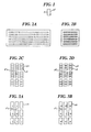
- Fig. 1 is a diagramatic view of a large pixel composed of small camera pixels for use in accordance with the method underlying the invention
- the invention embraces a method of increasing the processing speed of optical scanning in which an object is scanned by a camera to determine defects, features or differences, that comprises, scanning the objects to generate binary value small pixels corresponding to the presence or absence of physical characteristics; generating from the small pixels a set of larger pixels each constituted of a group of the small pixels; conveying to the larger pixels defect, feature or difference information contained in one or more of the small pixels constituting the same; and processing the larger pixels at a data rate or processing speed that is a multiple of that achievable in processing the small pixels, while maintaining the information from the scanning that is contained in the small pixels.
- Preferred and best mode embodiments and details will later be presented.
- circuit hoard inspection As an example, current high-speed inspection systems of the above-described and related types must be designed to detect very small defects, such as hairline breaks, hairline shorts, pinholes, specks and critical minute errors. To do so, very small picture elements must be chosen, referred to as pixels, that are sufficiently small to enable the detection of such small defects. Unfortunately, however, when pixel size is very small, and the objects such as the circuit boards are large, there are a very large number of pixels to process. To reduce such large numbers of pixels, and thus enhance the processing speed, the present invention provides a scheme whereby larger pixels are generated (actually groups of smaller pixels).
- Inspection is made of the information within the group of smaller pixels to determine whether the same contains a defect or region of difference from its surrounding pixels; and, if so, this information is conveyed to the larger pixel.
- the number of pixels is reduced by converting the small pixels into larger pixels or pixel groups, and the data rate is accordingly reduced while still maintaining the information contained in the small pixels through conveying such information to the large pixel group.
- Camera pixels P, Fig. 1 have binary values of 1 or 0 to denote the presence or absence of conducting material or other physical characteristics or features.
- the larger pixel P1 (shown composed of four camera pixels P), like the camera pixel P, has also a binary value of 1 or 0; but the binary value is computed in such a way as to accentuate in the large pixel P1 small defects or variations, so that they are detected by the shape-recognition algorithm, as of said Letters Patent, which will then process the larger pixels.
- Figs. 2A and 2B respectively show a pinhole in a printed circuit line (indicated by a 0) and a speck in the board laminate (indicated as a 1).
- a large pixel P1 one examines the neighborhood of at least an array of six-by-six camera pixels P which is equivalent to at least a set of three-by-three large pixels P1 Fig. 2C.
- the value of the neighborhood is said to be the majority value of the camera pixels surrounding the center four camera pixels. For example, with the pinhole, Fig. 2A, the majority equals a 1; and for the speck, Fig. 2D, the majority equals 0.
- the number of pixels that differ from the majority value are computed.
- the value of the center large pixel P c 1, Figs. 2C and 2D is then set equal to the opposite value of the neighborhood if a certain or some minimum number T of the pixels in the center group differ from the neighborhood to accentuate the pixel that is different. Otherwise, it is set equal to the same value as the neighborhood.
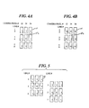
- the large pixels P1 will have the values shown in Fig. 3A, where the center larger pixel P c 1 is 0 because of the 0 information within the center larger pixel of Fig. 2C.
- the center pixel P c 1 of Fig. 3B for the case of the speck in the laminate, reflects by its 1 value, that information within the center large pixel P c 1 of Fig. 3B.
- Figs. 4A and 4B indicate the output values of the large pixels relative to camera line number and pixel timing for the respective pinhole and speck examples of respective Figs. 3A and 3B. Large pixels are shown computed on the occurrence of an even line (line numbers 2, 4, and 6) and pixel number.
- the pattern recognition processors of the present invention operate at the data rate of the large pixels P1, which is half the camera pixel data rate. This could correspond to, for example, 10 megahertz for a 20 megahertz camera. In addition, since the system must operate on images without missing lines, processor data can only be analyzed on alternate camera lines.
- the memory is subdivided into two halves; one for one camera path A, Fig. 6, and the other side or part of the memory would support camera path B.
- the two cameras A and B may be interleaved on alternate lines and place their data into corresponding M A and M B sides of memory such that the system would process data in the same mode and in conjunction with the same technique described in said Letters Patent and in the previously-mentioned Circuit One system.
- the smaller pixels P11-P66 make up the three-by-three larger pixels P1, with the neighborhood majority and center pixel value computation effected as before described; namely, the value of the center larger pixel P c 1 is not equal to the majority value if more than T pixels within the center group differ from the majority value.
- the two cameras are operating at a given data rate N; such as 20 megahertz.
- the data from the camera, Fig. 6, is subsampled into the larger pixel groups P1 to produce a reduction of at least a factor of two; so that the 20 megahertz data rate with the large pixels P1 is effectively a N/2 data rate, or 10 megahertz on every other line.
- the processor By interleaving the data from the two cameras (Multiplexer, Fig. 6) the processor only runs at a continuous 10 megahertz rate while both cameras A and B are continually running at the 20 megahertz data rate.
- two cameras at 20 megahertz each produce an effective, true scanning board speed of 40 megahertz, though the processor is only processing data at 10 megahertz.
- Figs. 2A-6 involve a general neighborhood of the set of three-by-three large pixels P1, corresponding to six-by-six small pixels
- other numbers may be used, such as a set of four-by-four large pixels, or five-by-five, as further examples; and the only thing that would increase is some of the processing hardware immediately used to compute the majority value. Since hardware, however, is becoming cheaper and more dense, it appears that in the immediate future, practice will not be limited to using the exemplary three-by-three large pixels.
- the value of the center larger pixel P c 1 is computed, it is stated that the value of the center pixel group is not equal to the majority if more than some predetermined number of pixels (T) contained within the center group differs from the majority value. This accentuates pixels that differ from their surroundings and which are frequently defects that it is desired to detect in the inspection process.
- T some predetermined number of pixels
- the rule may be set that for a large pixel group P1 to be different from its neighbor, a large number of small pixels P in that group must indeed be different from the neighbor; and if only one out of four pixels P is different (say constituting a very small pinhole), this will not be reflected at all, and the threshhold will accordingly be set.
- the exact opposite results i.e. finding a small pinhole wherein only one pixel differs from the majority.
- Another way of fine tuning the results involves selecting the size of the neighborhood. If we start with a large neighborhood, and the number of pixels equal to a 1 are approximately 50 percent, one can choose a smaller neighborhood that yields a better estimate of the data pixels surrounding the center pixel. For example, if the large neighborhood contains 6X6 (36) pixels and the number of data pixels equalling 1 are 17, a 4X4 (16 pixel) neighborhood may be selected to determine the majority value. In addition, one can also compute the majority pixel value of the 4 2X2 groups shown in Fig. 7A. These may be referred to as groups A, B, C, D, enlarging and surrounding the four corners of the center pixel group E, using these majority values to help determine the neighborhood majority value.
- the mechanism of selecting smaller neighborhoods to eliminate ambiguity increases the intelligence of the algorithm. If the number of pixels in the 6X6 group equal to a 1 are approximately 50%, then the majority value given by the smaller 4X4 local group is selected to yield a better estimate for the pixels around the center group E. If the value is not close to 50%, the binary value of the majority given for the 6X6 group is selected.
- FIG. 7 Shown in Fig. 7 is a block circuit diagram illustrating how the value of the center pixel group P c 1 is determined as a function of the majority neighborhood value, the value of the center pixels in the center group, and the variable threshhold T.
- a computation circuit block 10 called the majority neighborhood value computation, which determines whether the majority of binary pixels is indeed a 1 or a 0.
- the center pixel group P c 1 is accessed and as a function of the majority value. If the majority value is equal to 1, then the sum of points equalling a 0 in the center pixel group is computed in the summation circuit 12. If the majority value equals 0, then the sum of points equalling 1 in the center pixel group is computed.
- the output of the intelligent summing section 12 indicates the number of pixels which are not equal to the majority value.
- a comparison is then made in comparator 14 of the number of different pixels, with a threshhold input T that may be variable as a function of defect or detectable size, as before mentioned.
- the output of the comparator 14 that compares the majority of different pixels to their threshhold value T is equal to 1 if the number of pixels that differ from the majority exceeds the threshhold value.
- the output is 0, otherwise.
- the logical exclusive output of the comparator 14 is with the actual majority value itself, yielding the value of the center pixel group P c 1.
- center group P c 1 Whenever the number of differing pixels in that center group P c 1 exceeds the threshhold T, then the value of the center group is the opposite value of the threshhold; and, likewise, when the number of differing pixels is less than this threshhold T, the value of the center pixel remains the value of the majority.
- a larger neighborhood about the center group (A, B, C, D, Fig. 7a) may also be selected.
- pre-processor It is important to emphasize that what has been above described is in essence a pre-processor. It does not assume or make any assumptions as to the type of processing to be followed. Thus it can be used as a pre-processor with many types of apparatus, whether it be line width measurement, pattern recognition systems, a system that stores data and desires to decrease the number of data bits that are being stored or other similar applications.
- the invention provides a rather generic pre-processor that can be applied to a large number of such processing systems.
- a preferred method of implementation of the system of Fig. 7 used four CCD cameras A, B, C and D and eight memories ("MEM1" through “MEM8”). Each memory is capable of storing one CCD camera line of data.
- This implementation used 8Kx8 bit memories (type PC164 made by the Performance Company) and 2500 element CCD's (CCD Type 181 made by Fairchild Company).
- the first pixels of each CCD is stored. Pixels A00, B00 are stored into MEM1, and C00, D00 into MEM3, as shown in Fig. 8.
- the second pixel of each CCD is stored; A01, B01 into MEM2 and C01, D01 into MEM4, where C xy denotes camera C, line number x, pixel number y.
- Memories MEM1, 2, 3 and 4 are filled during the odd-numbered CCD scan lines.
- memories MEM 5, 6, 7 and 8 are filled during even-numbered CCD scan lines.
- new incoming camera pixels are stored into the free half of memories MEM 1, 2, 3 and 4, while reading out large pixel groups from the previously filled other half of the same memory, corresponding to cameras A and B.
- the memories (with a 25 nanosecond (ns) access time) are sufficiently fast to enable reading large pixel group data from one address and then writing new camera data into another address within one 100ns cycle. Two large pixel groups are read out each clock cycle yielding a 2:1 increase per CCD scan line.
- the readout format is shown in Fig. 9.
- new pixels are stored from cameras A, B, C, D into the free half of memories MEM 5, 6, 7 and 8, while reading out large pixels corresponding to cameras C and D.
- the total address space or length of each memory only needs to be one CCD line long since there are half as many large pixels as camera pixels per line. In general, this method can be expanded to handle more cameras by adding more memories.
- a vertical and horizontal delay line for example, fabricated using PC164 memories and 74374 type latches. These delay lines form the 6X6 pixel neighborhood shown in Fig. 7.
- the 36 total pixels are input to a programmable logic device (such as type EP1200 by Altera Company) which is programmed to compute the majority value of the neighborhood, and produce the value of the center pixel P C in Fig. 7, using the procedure described above.
Landscapes
- Engineering & Computer Science (AREA)
- Quality & Reliability (AREA)
- Computer Vision & Pattern Recognition (AREA)
- Physics & Mathematics (AREA)
- General Physics & Mathematics (AREA)
- Theoretical Computer Science (AREA)
- Investigating Materials By The Use Of Optical Means Adapted For Particular Applications (AREA)
Priority Applications (1)
| Application Number | Priority Date | Filing Date | Title |
|---|---|---|---|
| EP90304972A EP0455898A1 (fr) | 1990-05-09 | 1990-05-09 | Système d'inspection par balayage d'image |
Applications Claiming Priority (1)
| Application Number | Priority Date | Filing Date | Title |
|---|---|---|---|
| EP90304972A EP0455898A1 (fr) | 1990-05-09 | 1990-05-09 | Système d'inspection par balayage d'image |
Publications (1)
| Publication Number | Publication Date |
|---|---|
| EP0455898A1 true EP0455898A1 (fr) | 1991-11-13 |
Family
ID=8205414
Family Applications (1)
| Application Number | Title | Priority Date | Filing Date |
|---|---|---|---|
| EP90304972A Withdrawn EP0455898A1 (fr) | 1990-05-09 | 1990-05-09 | Système d'inspection par balayage d'image |
Country Status (1)
| Country | Link |
|---|---|
| EP (1) | EP0455898A1 (fr) |
Cited By (5)
| Publication number | Priority date | Publication date | Assignee | Title |
|---|---|---|---|---|
| EP0543629A1 (fr) * | 1991-11-19 | 1993-05-26 | E.I. Du Pont De Nemours And Company | Détection de défauts |
| EP0686932A3 (fr) * | 1994-03-17 | 1997-06-25 | Texas Instruments Inc | Sytème de vision à ordinateur pour chercher des objets rectangulaires trois-dimensionnels |
| EP0651264A3 (fr) * | 1993-10-28 | 1997-09-10 | Daimler Benz Aerospace Ag | Procédé de détection automatique des objets fixes ou en mouvement dans un environnement naturel d'une suite d'images en temps réel. |
| WO1998055959A1 (fr) * | 1997-06-04 | 1998-12-10 | Dirk Ernest Maria Van Dyck | Reconnaissance des formes a l'aide d'une correlation contextuelle |
| CN103776839A (zh) * | 2014-02-10 | 2014-05-07 | 宁波工程学院 | 一种新型表面裂纹检测算法 |
Citations (3)
| Publication number | Priority date | Publication date | Assignee | Title |
|---|---|---|---|---|
| EP0009674A1 (fr) * | 1978-10-02 | 1980-04-16 | International Business Machines Corporation | Appareil de traitement de données pour améliorer la lisibilité d'objets représentés dans une échelle modifiée |
| WO1984003784A1 (fr) * | 1983-03-21 | 1984-09-27 | Beltronics Inc | Procede et appareil d'inspection a haute vitesse en temps reel d'objets dans le but d'identifier ou reconnaitre des parties connues et inconnues de ces objets, y compris leurs defauts et autres |
| EP0228553A2 (fr) * | 1985-12-27 | 1987-07-15 | International Business Machines Corporation | Appareil et méthode de traitement d'images ayant des éléments d'images multivaleurs |
-
1990
- 1990-05-09 EP EP90304972A patent/EP0455898A1/fr not_active Withdrawn
Patent Citations (3)
| Publication number | Priority date | Publication date | Assignee | Title |
|---|---|---|---|---|
| EP0009674A1 (fr) * | 1978-10-02 | 1980-04-16 | International Business Machines Corporation | Appareil de traitement de données pour améliorer la lisibilité d'objets représentés dans une échelle modifiée |
| WO1984003784A1 (fr) * | 1983-03-21 | 1984-09-27 | Beltronics Inc | Procede et appareil d'inspection a haute vitesse en temps reel d'objets dans le but d'identifier ou reconnaitre des parties connues et inconnues de ces objets, y compris leurs defauts et autres |
| EP0228553A2 (fr) * | 1985-12-27 | 1987-07-15 | International Business Machines Corporation | Appareil et méthode de traitement d'images ayant des éléments d'images multivaleurs |
Cited By (8)
| Publication number | Priority date | Publication date | Assignee | Title |
|---|---|---|---|---|
| EP0543629A1 (fr) * | 1991-11-19 | 1993-05-26 | E.I. Du Pont De Nemours And Company | Détection de défauts |
| EP0651264A3 (fr) * | 1993-10-28 | 1997-09-10 | Daimler Benz Aerospace Ag | Procédé de détection automatique des objets fixes ou en mouvement dans un environnement naturel d'une suite d'images en temps réel. |
| EP0686932A3 (fr) * | 1994-03-17 | 1997-06-25 | Texas Instruments Inc | Sytème de vision à ordinateur pour chercher des objets rectangulaires trois-dimensionnels |
| WO1998055959A1 (fr) * | 1997-06-04 | 1998-12-10 | Dirk Ernest Maria Van Dyck | Reconnaissance des formes a l'aide d'une correlation contextuelle |
| BE1011191A4 (nl) * | 1997-06-04 | 1999-06-01 | Dyck Dirk Ernest Maria Van | Patroonherkenning met behulp van contextuele correlatie. |
| US6707941B1 (en) | 1997-06-04 | 2004-03-16 | Dirk Ernest Maria Van Dyck | Pattern recognition using contextual correlation |
| CN103776839A (zh) * | 2014-02-10 | 2014-05-07 | 宁波工程学院 | 一种新型表面裂纹检测算法 |
| CN103776839B (zh) * | 2014-02-10 | 2016-05-04 | 湖州师范学院 | 一种表面裂纹检测算法 |
Similar Documents
| Publication | Publication Date | Title |
|---|---|---|
| EP0041400B1 (fr) | Appareil et procédé de traitement des signaux d'image avec une résolution multiple | |
| CA1309502C (fr) | Methode et systeme pour ameliorer la qualite d'une image numerisee | |
| JP2702928B2 (ja) | 画像入力装置 | |
| EP0521662B1 (fr) | Amélioration de la segmentation automatique d'images | |
| EP0195372B1 (fr) | Méthode et dispositif pour former 3x3 zones d'éléments d'images modifications et contingents programmables de ces zones | |
| US4290084A (en) | Method and means for preserving original continuity/discontinuity among same colored pel clusters upon array compression | |
| US5046120A (en) | Method of and apparatus for increasing the processing speed in the scanning inspection of circuit boards and other objects | |
| EP0543629A1 (fr) | Détection de défauts | |
| JPH07117498B2 (ja) | 検査システム | |
| US5812704A (en) | Method and apparatus for image overlap processing | |
| EP0499875B1 (fr) | Procédé et dispositif pour obtenir une image binaire | |
| US5687252A (en) | Image processing apparatus | |
| US6878956B2 (en) | Apparatus and method for inspecting a surface of an inspection object | |
| EP0094824B1 (fr) | Dispositif de traitement d'image pour extraire continuellement des éléments de petites regions d'une image | |
| US6272260B1 (en) | Method of and apparatus for processing an image filter | |
| JPH02118886A (ja) | マスタ画像絵素との比較方法 | |
| US6192153B1 (en) | Image processing device | |
| CA2015162C (fr) | Methode et dispositif pour accroitre la vitesse de traitement dans l'inspection par exploration de cartes de circuits et autres objets | |
| US5062142A (en) | Data processor producing a medial axis representation of an extended region | |
| Baykal et al. | Detection of defects in textures with alignment error for real-time line-scan web inspection systems | |
| JP4653339B2 (ja) | 画像マッチング処理方法 | |
| JPH0332723B2 (fr) | ||
| US5911014A (en) | Method and apparatus for extracting an abnormal pattern | |
| JP2841373B2 (ja) | パターン検査装置 | |
| Spitz | Correcting for variable skew in document images |
Legal Events
| Date | Code | Title | Description |
|---|---|---|---|
| PUAI | Public reference made under article 153(3) epc to a published international application that has entered the european phase |
Free format text: ORIGINAL CODE: 0009012 |
|
| AK | Designated contracting states |
Kind code of ref document: A1 Designated state(s): AT BE CH DE ES FR GB GR IT LI NL SE |
|
| 17P | Request for examination filed |
Effective date: 19920505 |
|
| 17Q | First examination report despatched |
Effective date: 19941006 |
|
| STAA | Information on the status of an ep patent application or granted ep patent |
Free format text: STATUS: THE APPLICATION IS DEEMED TO BE WITHDRAWN |
|
| 18D | Application deemed to be withdrawn |
Effective date: 19951201 |