EP0455963A1 - Dispositif et procédé de transformation d'un premier signal utile de la trame d'un premier signal numérique au moyen de technique de justification d'impulsion dans la trame d'un second signal numérique - Google Patents
Dispositif et procédé de transformation d'un premier signal utile de la trame d'un premier signal numérique au moyen de technique de justification d'impulsion dans la trame d'un second signal numérique Download PDFInfo
- Publication number
- EP0455963A1 EP0455963A1 EP91104282A EP91104282A EP0455963A1 EP 0455963 A1 EP0455963 A1 EP 0455963A1 EP 91104282 A EP91104282 A EP 91104282A EP 91104282 A EP91104282 A EP 91104282A EP 0455963 A1 EP0455963 A1 EP 0455963A1
- Authority
- EP
- European Patent Office
- Prior art keywords
- frame
- digital signal
- fill level
- stuffing
- signal
- Prior art date
- Legal status (The legal status is an assumption and is not a legal conclusion. Google has not performed a legal analysis and makes no representation as to the accuracy of the status listed.)
- Granted
Links
- 238000000034 method Methods 0.000 title claims abstract description 18
- 230000001131 transforming effect Effects 0.000 title 1
- 230000004913 activation Effects 0.000 claims description 4
- 238000005516 engineering process Methods 0.000 claims description 4
- 238000013507 mapping Methods 0.000 claims description 4
- 238000005070 sampling Methods 0.000 claims 1
- 230000001419 dependent effect Effects 0.000 abstract 1
- 230000005540 biological transmission Effects 0.000 description 1
- 238000011161 development Methods 0.000 description 1
- 230000018109 developmental process Effects 0.000 description 1
- 238000010586 diagram Methods 0.000 description 1
- 238000011084 recovery Methods 0.000 description 1
Images
Classifications
-
- H—ELECTRICITY
- H04—ELECTRIC COMMUNICATION TECHNIQUE
- H04J—MULTIPLEX COMMUNICATION
- H04J3/00—Time-division multiplex systems
- H04J3/02—Details
- H04J3/06—Synchronising arrangements
- H04J3/07—Synchronising arrangements using pulse stuffing for systems with different or fluctuating information rates or bit rates
- H04J3/076—Bit and byte stuffing, e.g. SDH/PDH desynchronisers, bit-leaking
Definitions
- the invention relates to an arrangement for mapping a useful signal from the frame of a first digital signal with a first bit rate using pulse stuffing technology into the frame of a second digital signal with a second bit rate according to the preamble of claim 1 and a method for mapping a useful signal from the frame of a first digital signal with a first bit rate using pulse stuffing technology in the frame of a second digital signal with a second bit rate according to the preamble of claim 7.
- the method of pulse plugging is used. It is used in particular when time-division multiplexing plesiochronous signals are bundled in multiplex devices and when a signal with a first bit rate is mapped into a switching frame with a second, higher bit rate for the purpose of synchronization.
- the impulse plug two variants of the impulse plug are known: the positive plug and the positive-zero-negative plug.
- an input signal with a first bit rate is mapped into an output signal with a second bit rate.
- the input signal is written into an elastic memory, the addressing being carried out using a write counter which counts with a clock pulse which corresponds to the first bit rate.
- the data are then read out again from the elastic memory, a read counter also running. If the bit rates of the output and input signals differ, stuffing operations are required.
- a phase comparator compares the phases of the write counter and read counter. If the phase difference deviates from its target value by a certain value, a control circuit initiates a stuffing process. With positive stuffing, a stuff bit is included in the output signal at a defined point.
- an information bit is transmitted from the elastic memory in an auxiliary channel.
- the information as to whether a useful information bit or a stuffing bit is transmitted in a stuffable period (positive stuffing point) or whether an information bit (negative stuffing place) is transmitted in the auxiliary channel is transmitted in the so-called stuffing information bits of the auxiliary channel. If the original digital signal is to be recovered, the tamping operations must be undone. An important point is the clock recovery. The clock is usually only incompletely smoothed in the desynchronizer and differs from the original clock by a phase modulation, the waiting time jitter.
- the useful signal is first recovered using a phase locked loop.
- the recovered useful signal is subject to a waiting time jitter. This recovered useful signal can then be mapped into the frame of the second digital signal.
- the invention has for its object to provide an arrangement with which it is possible to directly plug a useful signal from a first digital signal with a first frame and a first bit rate into a second digital signal with a second frame and a second bit rate.
- the bit rate of the useful signal is lower than the bit rates of the two digital signals.
- a desynchronizer and then a synchronizer, each with an elastic memory, are not used, but only an elastic memory is necessary. In addition, no analog phase locked loop is necessary.
- the average fill level of the elastic store is determined, from which the decision to fill can be obtained. Whether there is a stop depends on whether the average fill level exceeds or falls below certain threshold values.
- the information as to whether or not stuffing has been done is transmitted in 1-bit steps from the synchronizer to the desynchronizer using the stuffing information. This can result in a high waiting time jitter. If the output signal of the arrangement has sufficient free space so that additional information is transmitted, then the average fill level of the elastic memory can be transmitted to the desynchronizer. If this average fill level is used to control the PLL arrangement in the desynchronizer, phase tracking takes place and the waiting time jitter in the desynchronizer can be reduced. To carry out this method, it is necessary to precisely determine the average fill level of the elastic memory of the arrangement.
- the arrangement according to the invention and the method according to the invention for determining stuffing information thus make it possible to reduce the waiting time jitter by transmitting the average fill level.
- a method for finding darning decisions is specified, which is particularly inexpensive when the mean fill level of the storage is determined on the basis of the desired reduction in the waiting time jitter.
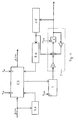
- the arrangement is supplied with the first digital signal D, which contains a useful signal N.
- the useful signal N is written into an elastic memory ES with gaps.
- a frame detector RD detects the frame of the digital signal D and controls the write activation of the elastic memory ES.
- the useful signal N which is inserted into the frame of a digital signal A, is read out gently from the elastic memory ES.
- the digital signal A has a stuffing frame frequency t SR . Each darning frame can be darned once.
- a frame generator RG is provided which generates the frame of the digital signal A and controls the read activation of the elastic memory ES.
- the current fill level of the elastic store ES is determined.
- the current fill levels are accumulated in an integrator I. This happens once for each tamping frame, that is, with the frequency of the tamping frame t SR , which is fed to the integrator. When accumulating, it is not necessary to provide all comparison values as summands. However, it makes sense to distribute the summands equidistantly in the context of the digital signal A.
- the output signal of the integrator I is the average fill level of the elastic memory ES of the nth stuffing frame. This signal is fed to a digital low-pass filter T.
- the digital low-pass filter is also clocked at the stuffing frame frequency t SR .
- Its output signal is the average filtered fill level of the elastic memory of the nth stuffing frame.
- the middle one filtered memory fill level can be transmitted to the desynchronizer as additional information in the context of digital signal A.
- the mean filtered memory fill level of the nth stuffing frame is fed to a decision maker SE, which makes the stuffing decision depending on the output signal of the low-pass filter T.
- the justification decision is fed to the frame generator RG in the form of a correction value. It is also applied to the digital low pass to correct the low pass output.
- a darning decision is made as follows: The darning is positive if the mean filtered storage level of the nth darning frame is smaller than a lower one Threshold for the average storage level S u is.
- the negative is stuffed when the mean filtered storage level of the nth stuffing frame is greater than the upper threshold for the mean storage level S o . If the mean filtered storage level of the nth tamping frame lies between the upper threshold S o and the lower threshold S u , no tamping is necessary. With positive tamping, the correction value is 1, with negative tamping -1 and if no tamping is carried out, the correction value is 0.
- the relationship between the mean filtered storage level of the nth tamping frame and the correction value for the nth tamping frame, as well as the tamping process in The nth darning frame is shown in the following table.
- the sawtooth-shaped course of the mean storage level is restored.
- the necessary components which are filtered away from the low-pass filter, have to be added again at the adder of the low-pass filter.
- Feeding in the correction value at the low-pass adder generates the components of the sawtooth at the low-pass output by feedback and thus the desired course of the memory fill level.
- the support points for determining the average storage level are distributed over the entire tamping frame in order to minimize the noise amplitude caused by the different frame frequencies.
Landscapes
- Engineering & Computer Science (AREA)
- Computer Networks & Wireless Communication (AREA)
- Signal Processing (AREA)
- Time-Division Multiplex Systems (AREA)
- Synchronisation In Digital Transmission Systems (AREA)
Applications Claiming Priority (2)
| Application Number | Priority Date | Filing Date | Title |
|---|---|---|---|
| DE4014815A DE4014815A1 (de) | 1990-05-09 | 1990-05-09 | Anordnung und verfahren zum abbilden eines ersten nutzsignals aus dem rahmen eines ersten digitalsignals mittels impulsstopftechnik in den rahmen eines zweiten digitalsignals |
| DE4014815 | 1990-05-09 |
Publications (3)
| Publication Number | Publication Date |
|---|---|
| EP0455963A1 true EP0455963A1 (fr) | 1991-11-13 |
| EP0455963B1 EP0455963B1 (fr) | 1994-11-30 |
| EP0455963B2 EP0455963B2 (fr) | 1998-11-18 |
Family
ID=6405995
Family Applications (1)
| Application Number | Title | Priority Date | Filing Date |
|---|---|---|---|
| EP91104282A Expired - Lifetime EP0455963B2 (fr) | 1990-05-09 | 1991-03-20 | Dispositif et procédé de transformation d'un premier signal utile de la trame d'un premier signal numérique au moyen de technique de justification d'impulsion dans la trame d'un second signal numérique |
Country Status (2)
| Country | Link |
|---|---|
| EP (1) | EP0455963B2 (fr) |
| DE (2) | DE4014815A1 (fr) |
Cited By (3)
| Publication number | Priority date | Publication date | Assignee | Title |
|---|---|---|---|---|
| US5598445A (en) * | 1994-03-28 | 1997-01-28 | Alcatel N.V. | Jitter reduction system in digital demultiplexers |
| DE19653470A1 (de) * | 1996-12-20 | 1998-06-25 | Siemens Ag | Verfahren und Anordnung zur Taktrückgewinnung aus einem Digitalsignal |
| DE19732943A1 (de) * | 1997-07-31 | 1999-02-04 | Alsthom Cge Alcatel | Verfahren und Komponente zum Ausgleich von Frequenz- und Phasenschwankungen |
Families Citing this family (3)
| Publication number | Priority date | Publication date | Assignee | Title |
|---|---|---|---|---|
| DE4205623B4 (de) * | 1992-02-25 | 2006-06-29 | Philips Intellectual Property & Standards Gmbh | Leitungsendgerät |
| DE19509484A1 (de) * | 1995-03-16 | 1996-09-19 | Deutsche Telekom Ag | Verfahren zur empfangsseitigen Taktrückgewinnung für Digitalsignale |
| DE10128396B4 (de) | 2001-06-12 | 2005-02-24 | Infineon Technologies Ag | Verfahren und Schaltungsanordnung zum Übertragen von Daten von ein mit einem ersten Takt betriebenes System an ein mit einem zweiten Takt betriebenes System |
Citations (3)
| Publication number | Priority date | Publication date | Assignee | Title |
|---|---|---|---|---|
| EP0158302A2 (fr) * | 1984-04-06 | 1985-10-16 | Nec Corporation | Récepteur capable d'établir rapidement la synchronisation de trame stable |
| EP0165619A2 (fr) * | 1984-06-22 | 1985-12-27 | Nec Corporation | Circuit pour récepteur synchrone de données |
| US4764941A (en) * | 1987-05-22 | 1988-08-16 | American Telephone And Telegraph Company, At&T Bell Laboratories | Digital frame synchronizer |
-
1990
- 1990-05-09 DE DE4014815A patent/DE4014815A1/de not_active Withdrawn
-
1991
- 1991-03-20 DE DE59103621T patent/DE59103621D1/de not_active Expired - Fee Related
- 1991-03-20 EP EP91104282A patent/EP0455963B2/fr not_active Expired - Lifetime
Patent Citations (3)
| Publication number | Priority date | Publication date | Assignee | Title |
|---|---|---|---|---|
| EP0158302A2 (fr) * | 1984-04-06 | 1985-10-16 | Nec Corporation | Récepteur capable d'établir rapidement la synchronisation de trame stable |
| EP0165619A2 (fr) * | 1984-06-22 | 1985-12-27 | Nec Corporation | Circuit pour récepteur synchrone de données |
| US4764941A (en) * | 1987-05-22 | 1988-08-16 | American Telephone And Telegraph Company, At&T Bell Laboratories | Digital frame synchronizer |
Non-Patent Citations (3)
| Title |
|---|
| DIGITALE VERMITTLUNGSTECHNIK, 1981, R. Oldenbourg Verlag MÙnchen Wien H. BESIER et al. Seiten 137-144 * |
| FREQUENZ, Band 32, Nr. 10, Oktober 1978, Berlin, DE F. K¨HLE, K. LANG "Positiv- Null-Negativ-Stopftechnik fÙr die MultiplexÙbertragung plesiochroner Datensignale" Seiten 281-287 * |
| THE BELL SYSTEM TECHNICAL JOURNAL, Band 51, Nr. 1, JÛnner 1972, New York, US D.L. DUTTWEILER "Waiting Time Jitter" Seiten 165-207 * |
Cited By (4)
| Publication number | Priority date | Publication date | Assignee | Title |
|---|---|---|---|---|
| US5598445A (en) * | 1994-03-28 | 1997-01-28 | Alcatel N.V. | Jitter reduction system in digital demultiplexers |
| DE19653470A1 (de) * | 1996-12-20 | 1998-06-25 | Siemens Ag | Verfahren und Anordnung zur Taktrückgewinnung aus einem Digitalsignal |
| DE19653470C2 (de) * | 1996-12-20 | 1998-10-08 | Siemens Ag | Verfahren und Anordnung zur Taktrückgewinnung aus einem Digitalsignal |
| DE19732943A1 (de) * | 1997-07-31 | 1999-02-04 | Alsthom Cge Alcatel | Verfahren und Komponente zum Ausgleich von Frequenz- und Phasenschwankungen |
Also Published As
| Publication number | Publication date |
|---|---|
| DE59103621D1 (de) | 1995-01-12 |
| EP0455963B2 (fr) | 1998-11-18 |
| DE4014815A1 (de) | 1991-11-14 |
| EP0455963B1 (fr) | 1994-11-30 |
Similar Documents
| Publication | Publication Date | Title |
|---|---|---|
| DE69221101T2 (de) | Desynchronisierer von synchronen digitalen Signalen zu asynchronen digitalen Signalen | |
| DE69831473T2 (de) | Verfahren und Vorrichtung zum Multiplexen und Demultiplexen digitaler Signalströme | |
| EP0503732B1 (fr) | Méthode et système de transmission pour la hiérarchie numérique synchrone | |
| DE69217526T2 (de) | Linearer In-line-Desynchronisierer | |
| DE69227820T2 (de) | Sonet DS-N-Desynchronisiereinrichtung | |
| DE69330492T2 (de) | Desynchronisierer und verfahren zur unterdrückung des zeigerzitterns in einen desynchronisierer | |
| DE69132247T2 (de) | Phasenverriegelte Schleifenanordnung | |
| EP0708541B1 (fr) | Système de transmission avec une boucle de commande | |
| EP0475498B1 (fr) | Circuit d'adaption du débit binaire de deux signaux numériques | |
| DE69323071T2 (de) | Anordnung von digitalen Phasenregelschleifen | |
| DE3308903A1 (de) | Adaptive schwellenwertvorrichtung | |
| DE4013317C2 (fr) | ||
| DE3140683C2 (de) | Zeitdehnungsschaltkreis für Wiedergabesysteme | |
| DE19515344A1 (de) | Synchrones digitales Übertragungssystem | |
| EP0455963B1 (fr) | Dispositif et procédé de transformation d'un premier signal utile de la trame d'un premier signal numérique au moyen de technique de justification d'impulsion dans la trame d'un second signal numérique | |
| DE4014814C2 (fr) | ||
| DE4101270A1 (de) | Verfahren zur uebertragung von digitalsignalen | |
| DE19820572A1 (de) | Desynchronisiereinrichtung für ein synchrones digitales Nachrichtenübertragungssystem | |
| DE4014800C2 (de) | Verfahren zur Ermittlung des mittleren Füllstandes eines elastischen Speichers und Anordnung zur Durchführung des Verfahrens | |
| DE2822873C3 (de) | Schaltung zur Verminderung von Dropout-Störungen in einem Videosignal | |
| EP0461703B1 (fr) | Circuit d'adaption de débit binaire | |
| DE19820658A1 (de) | Digitale Phasenregelschleife für Niedriggeschwindigkeitssignalschaltsystem mit plesiochroner digitaler Hierarchie | |
| EP0455865B1 (fr) | Circuit pour insérer un signal utile d'une trâme d'un premier signal numérique utilisant la technique de bourrage dans une trâme d'un deuxième signal numérique et utilisation d'un tel circuit | |
| DE4339586B4 (de) | Übertragungssystem | |
| DE69721563T2 (de) | Digitale phasenregelschleife und verfahren zu ihrer steuerung sowie methode und empfangsschaltung zur desynchronisation in einem digitalen übertragungssystem |
Legal Events
| Date | Code | Title | Description |
|---|---|---|---|
| PUAI | Public reference made under article 153(3) epc to a published international application that has entered the european phase |
Free format text: ORIGINAL CODE: 0009012 |
|
| AK | Designated contracting states |
Kind code of ref document: A1 Designated state(s): DE FR GB IT SE |
|
| 17P | Request for examination filed |
Effective date: 19910930 |
|
| 17Q | First examination report despatched |
Effective date: 19931018 |
|
| GRAA | (expected) grant |
Free format text: ORIGINAL CODE: 0009210 |
|
| ITF | It: translation for a ep patent filed | ||
| AK | Designated contracting states |
Kind code of ref document: B1 Designated state(s): DE FR GB IT SE |
|
| REF | Corresponds to: |
Ref document number: 59103621 Country of ref document: DE Date of ref document: 19950112 |
|
| EAL | Se: european patent in force in sweden |
Ref document number: 91104282.8 |
|
| ET | Fr: translation filed | ||
| GBT | Gb: translation of ep patent filed (gb section 77(6)(a)/1977) |
Effective date: 19950210 |
|
| PLBI | Opposition filed |
Free format text: ORIGINAL CODE: 0009260 |
|
| 26 | Opposition filed |
Opponent name: ALCATEL N.V. Effective date: 19950830 |
|
| PLBF | Reply of patent proprietor to notice(s) of opposition |
Free format text: ORIGINAL CODE: EPIDOS OBSO |
|
| RAP2 | Party data changed (patent owner data changed or rights of a patent transferred) |
Owner name: ROBERT BOSCH GMBH |
|
| PLAW | Interlocutory decision in opposition |
Free format text: ORIGINAL CODE: EPIDOS IDOP |
|
| PLAW | Interlocutory decision in opposition |
Free format text: ORIGINAL CODE: EPIDOS IDOP |
|
| PUAH | Patent maintained in amended form |
Free format text: ORIGINAL CODE: 0009272 |
|
| STAA | Information on the status of an ep patent application or granted ep patent |
Free format text: STATUS: PATENT MAINTAINED AS AMENDED |
|
| 27A | Patent maintained in amended form |
Effective date: 19981118 |
|
| AK | Designated contracting states |
Kind code of ref document: B2 Designated state(s): DE FR GB IT SE |
|
| GBTA | Gb: translation of amended ep patent filed (gb section 77(6)(b)/1977) | ||
| ITF | It: translation for a ep patent filed | ||
| REG | Reference to a national code |
Ref country code: GB Ref legal event code: 732E |
|
| ET3 | Fr: translation filed ** decision concerning opposition | ||
| REG | Reference to a national code |
Ref country code: GB Ref legal event code: IF02 |
|
| PGFP | Annual fee paid to national office [announced via postgrant information from national office to epo] |
Ref country code: GB Payment date: 20020215 Year of fee payment: 12 |
|
| PGFP | Annual fee paid to national office [announced via postgrant information from national office to epo] |
Ref country code: SE Payment date: 20020306 Year of fee payment: 12 |
|
| PGFP | Annual fee paid to national office [announced via postgrant information from national office to epo] |
Ref country code: FR Payment date: 20020312 Year of fee payment: 12 |
|
| PGFP | Annual fee paid to national office [announced via postgrant information from national office to epo] |
Ref country code: DE Payment date: 20020327 Year of fee payment: 12 |
|
| PG25 | Lapsed in a contracting state [announced via postgrant information from national office to epo] |
Ref country code: GB Free format text: LAPSE BECAUSE OF NON-PAYMENT OF DUE FEES Effective date: 20030320 |
|
| PG25 | Lapsed in a contracting state [announced via postgrant information from national office to epo] |
Ref country code: SE Free format text: LAPSE BECAUSE OF NON-PAYMENT OF DUE FEES Effective date: 20030321 |
|
| PG25 | Lapsed in a contracting state [announced via postgrant information from national office to epo] |
Ref country code: DE Free format text: LAPSE BECAUSE OF NON-PAYMENT OF DUE FEES Effective date: 20031001 |
|
| EUG | Se: european patent has lapsed | ||
| GBPC | Gb: european patent ceased through non-payment of renewal fee |
Effective date: 20030320 |
|
| PG25 | Lapsed in a contracting state [announced via postgrant information from national office to epo] |
Ref country code: FR Free format text: LAPSE BECAUSE OF NON-PAYMENT OF DUE FEES Effective date: 20031127 |
|
| REG | Reference to a national code |
Ref country code: FR Ref legal event code: ST |
|
| PG25 | Lapsed in a contracting state [announced via postgrant information from national office to epo] |
Ref country code: IT Free format text: LAPSE BECAUSE OF NON-PAYMENT OF DUE FEES;WARNING: LAPSES OF ITALIAN PATENTS WITH EFFECTIVE DATE BEFORE 2007 MAY HAVE OCCURRED AT ANY TIME BEFORE 2007. THE CORRECT EFFECTIVE DATE MAY BE DIFFERENT FROM THE ONE RECORDED. Effective date: 20050320 |