EP0455963B1 - Arrangement and method for transforming a first useful signal from the frame of a first digital signal by pulse stuffing techniques to the frame of a second digital signal - Google Patents
Arrangement and method for transforming a first useful signal from the frame of a first digital signal by pulse stuffing techniques to the frame of a second digital signal Download PDFInfo
- Publication number
- EP0455963B1 EP0455963B1 EP91104282A EP91104282A EP0455963B1 EP 0455963 B1 EP0455963 B1 EP 0455963B1 EP 91104282 A EP91104282 A EP 91104282A EP 91104282 A EP91104282 A EP 91104282A EP 0455963 B1 EP0455963 B1 EP 0455963B1
- Authority
- EP
- European Patent Office
- Prior art keywords
- frame
- storage device
- digital signal
- stuffing
- elastic storage
- Prior art date
- Legal status (The legal status is an assumption and is not a legal conclusion. Google has not performed a legal analysis and makes no representation as to the accuracy of the status listed.)
- Expired - Lifetime
Links
- 238000000034 method Methods 0.000 title claims description 19
- 230000001131 transforming effect Effects 0.000 title 1
- 238000013507 mapping Methods 0.000 claims description 5
- 230000004913 activation Effects 0.000 claims description 3
- 238000005516 engineering process Methods 0.000 description 3
- 230000005540 biological transmission Effects 0.000 description 1
- 238000011161 development Methods 0.000 description 1
- 230000018109 developmental process Effects 0.000 description 1
- 238000010586 diagram Methods 0.000 description 1
- 238000011084 recovery Methods 0.000 description 1
Images
Classifications
-
- H—ELECTRICITY
- H04—ELECTRIC COMMUNICATION TECHNIQUE
- H04J—MULTIPLEX COMMUNICATION
- H04J3/00—Time-division multiplex systems
- H04J3/02—Details
- H04J3/06—Synchronising arrangements
- H04J3/07—Synchronising arrangements using pulse stuffing for systems with different or fluctuating information rates or bit rates
- H04J3/076—Bit and byte stuffing, e.g. SDH/PDH desynchronisers, bit-leaking
Definitions
- the invention relates to an arrangement for mapping a useful signal from the frame of a first digital signal with a first bit rate using pulse stuffing technology into the frame of a second digital signal with a second bit rate according to the preamble of claim 1 and a method for mapping a useful signal from the frame of a first digital signal with a first bit rate using pulse stuffing technology in the frame of a second digital signal with a second bit rate according to the preamble of claim 7.
- the method of pulse plugging is used particularly when time-division multiplexing plesiochronous signals are multiplexed and when a signal with a first bit rate is mapped into a switching frame with a second, higher bit rate for the purpose of synchronization.
- the impulse plug two variants of the impulse plug are known: the positive plug and the positive-zero-negative plug.
- an input signal with a first bit rate is mapped into an output signal with a second bit rate.
- the input signal is written into an elastic memory, the addressing being carried out using a write counter which counts with a clock pulse which corresponds to the first bit rate.
- the data are then read out again from the elastic memory, a read counter also running.
- stuffing operations are required.
- a phase comparator compares the phases of the write counter and read counter. If the phase difference deviates from its desired value by a certain value, a control circuit initiates a stuffing process. With positive stuffing, a stuff bit is included in the output signal at a defined point.
- an information bit is transmitted from the elastic memory in an auxiliary channel.
- the information as to whether a useful information bit or a stuffing bit is transmitted in a stuffable period (positive stuffing point) or whether an information bit (negative stuffing place) is transmitted in the auxiliary channel is transmitted in the so-called stuffing information bits of the auxiliary channel. If the original digital signal is to be recovered, the tamping operations must be undone. An important point is the clock recovery. The clock is usually only incompletely smoothed in the desynchronizer and differs from the original clock by a phase modulation, the waiting time jitter.
- the useful signal is first recovered using a phase locked loop.
- the recovered useful signal is subject to a waiting time jitter. This recovered useful signal can then be mapped into the frame of the second digital signal.
- the invention has for its object to provide an arrangement with which it is possible to plug a useful signal from a first digital signal with a first frame and a first bit rate directly into a second digital signal with a second frame and a second bit rate.
- the bit rate of the useful signal is lower than the bit rates of the two digital signals.
- a desynchronizer and then a synchronizer, each with an elastic memory, is not used, but only an elastic memory is necessary.
- no analog phase locked loop is necessary.
- the average fill level of the elastic store is determined, from which the darning decision can be obtained. Whether a stop is made depends on whether the average fill level exceeds or falls below certain threshold values.
- the information as to whether or not the tamping has been done is made in 1-bit steps the stuffing information is transferred from the synchronizer to the desynchronizer. This can result in a high waiting time jitter. If the output signal of the arrangement has sufficient free space so that additional information is transmitted, the average fill level of the elastic memory can be transmitted to the desynchronizer. If this average fill level is used to control the PLL arrangement in the desynchronizer, phase tracking takes place and the waiting time jitter in the desynchronizer can be reduced. To carry out this method, it is necessary to precisely determine the average fill level of the elastic memory of the arrangement.
- the arrangement according to the invention and the method according to the invention for determining stuffing information therefore make it possible to reduce the waiting time jitter by transmitting the average fill level.
- a method for finding stuffing decisions is specified, which is particularly inexpensive when the average fill level of the storage is determined on the basis of the desired reduction in the waiting time jitter.
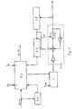
- Figure 1 shows a block diagram of an arrangement according to the invention.
- the arrangement is supplied with the first digital signal D, which contains a useful signal N.
- the useful signal N is written into an elastic memory ES with gaps.
- a frame detector RD detects the frame of the digital signal D and controls the write activation of the elastic memory ES.
- the useful signal N which is inserted into the frame of a digital signal A, is read out gently from the elastic memory ES.
- the digital signal A has a stuffing frame frequency t sR . Each darning frame has the option of darning once.
- a frame generator RG is provided which generates the frame of the digital signal A and controls the read activation of the elastic memory ES.
- the current level of the elastic store ES is determined.
- the current fill levels are accumulated in an integrator I. This is done once for each stuffing frame, that is, with the frequency of the stuffing frame t SR , which is fed to the integrator.
- the output signal of the integrator 1 is the average fill level of the elastic memory ES of the nth stuffing frame. This signal is fed to a digital low-pass filter T.
- the digital low-pass filter is also clocked at the stuffing frame frequency t sR .
- Its output signal is the average filtered fill level of the elastic memory of the nth stuffing frame.
- the average filtered memory fill level can be transmitted to the desynchronizer as additional information in the context of digital signal A.
- the average filtered memory fill level of the nth stuffing frame is fed to a decision maker SE, which makes the stuffing decision depending on the output signal of the low-pass filter T.
- the justification decision is fed to the frame generator RG in the form of a correction value. It is also applied to the digital low pass to correct the low pass output.
- a darning decision is made as follows: The darning is positive if the mean filtered storage level of the nth darning frame is smaller than a lower one
- Threshold for the mean storage level S u is.
- the negative is stuffed if the mean filtered storage level of the nth stuffing frame is greater than the upper threshold for the mean storage level S o . If the mean filtered storage level of the nth tamping frame lies between the upper threshold S o and the lower threshold S u , no tamping is necessary.
- the correction value is 1, with negative tamping -1 and if no tamping is carried out, the correction value is 0.
- the relationship between the mean filtered storage level of the nth tamping frame and the correction value for the nth tamping frame, as well as the tamping process in The nth darning frame is shown in the following table.
- the sawtooth-shaped course of the mean storage level is restored.
- the necessary components that are removed from the low-pass filter must be added again at the low-pass filter adder. Feeding in the correction value at the adder of the low-pass filter generates the components of the sawtooth at the low-pass filter output by feedback and thus the desired course of the memory fill level.
- the support points for determining the average storage level are distributed over the entire tamping frame in order to minimize the noise amplitude caused by the different frame frequencies.
Landscapes
- Engineering & Computer Science (AREA)
- Computer Networks & Wireless Communication (AREA)
- Signal Processing (AREA)
- Time-Division Multiplex Systems (AREA)
- Synchronisation In Digital Transmission Systems (AREA)
Description
Anordnung und Verfahren zum Abbilden eines ersten Nutzsignals aus dem Rahmen eines ersten Digitalsignals mittels Impulsstopftechnik in den Rahmen eines zweiten DigitalsignalsArrangement and method for mapping a first useful signal from the frame of a first digital signal into the frame of a second digital signal using pulse stuffing technology
Die Erfindung betrifft eine Anordnung zum Abbilden eines Nutzsignals aus dem Rahmen eines ersten Digitalsignals mit einer ersten Bitrate mittels Impulsstopftechnik in den Rahmen eines zweiten Digitalsignals mit einer zweiten Bitrate nach dem Oberbegriff des Patentanspruches 1 und ein Verfahren zum Abbilden eines Nutzsignals aus dem Rahmen eines ersten Digitalsignals mit einer ersten Bitrate mittels Impulsstopftechnik in den Rahmen eines zweiten Digitalsignals mit einer zweiten Bitrate gemäß dem Oberbegriff des Patentanspruches 7.The invention relates to an arrangement for mapping a useful signal from the frame of a first digital signal with a first bit rate using pulse stuffing technology into the frame of a second digital signal with a second bit rate according to the preamble of
Wenn ein gegebenes Digitalsignal mit einer anderen als mit seiner ursprünglichen Bitrate übertragen werden soll, dann wird das verfahren des Impulsstopfens eingesetzt. Es wird insbesondere dann angewandt, wenn plesiochrone Signale im Zeitmultiplex in Multiplexgeräten gebündelt werden und wenn ein Signal mit einer ersten Bitrate zum Zwecke der Synchronisierung in einen Durchschalterahmen mit einerzweiten, höheren Bitrate abgebildet wird. Im wesentlichen sind zwei Varianten des Impulsstopfens bekannt: Das Positiv-Stopfen und das Positiv-Null-Negativ-Stopfen.If a given digital signal is to be transmitted with a bit rate other than its original, then the method of pulse plugging is used. It is used particularly when time-division multiplexing plesiochronous signals are multiplexed and when a signal with a first bit rate is mapped into a switching frame with a second, higher bit rate for the purpose of synchronization. Basically two variants of the impulse plug are known: the positive plug and the positive-zero-negative plug.
Aus Duttweiler D.L., "Waiting Time Jitter", The BELL System Technical Journal, Vol. 51, No. 1, 1972, S. 165-207 ist ein Synchronisierer und ein Desynchronisierer für Positiv-Stopfen beschrieben.From Duttweiler D.L., "Waiting Time Jitter", The BELL System Technical Journal, Vol. 51, No. 1, 1972, pp. 165-207 describes a synchronizer and a desynchronizer for positive stuffing.
Aus dem Artikel von Kühne F. und Lang K., "Positiv-Null-Negativ-Stopftechnik für Multiplexübertragung plesiochroner Signale", Frequenz, Bd. 32, Nr. 10, 1978, S.281-287 ist ein Synchronisierer und ein Desynchronisiererfürdas Positiv-Null-Negativ-Stopfen bekannt.From the article by Kuehne F. and Lang K., "positive-zero-negative stuffing technique for multiplex transmission of plesiochronous signals", frequency, vol. 32, no. 10, 1978, p.281-287 is a synchronizer and a desynchronizer for the positive -Null negative plug known.
In beiden Fällen wird ein Eingangssignal mit einer ersten Bitrate in ein Ausgangssignal mit einer zweiten Bitrate abgebildet. Das Eingangssignal wird dazu in einen elastischen Speicher eingeschrieben, wobei die Adressierung mit einem Schreibzähler, der mit einem Takt zählt, der der ersten Bitrate entspricht, erfolgt. Für das Ausgangssignal werden die Daten dann aus dem elastischen Speicher wieder ausgelesen, wobei ein Lesezähler mitläuft. Wenn die Bitraten von Ausgangs- und Eingangssignal voneinander abweichen, sind Stopfvorgänge erforderlich. Ein Phasenvergleichervergleicht die Phasen von Schreibzähler und Lesezähler. Weicht die Phasendifferenz um einen bestimmten Wert von ihrem Sollwert ab, so veranlaßt eine Steuerschaltung einen Stopfvorgang. Beim Positiv-Stopfen wird an einer definierten Stelle ein Stopfbit in das Ausgangssignal übernommen. Beim Negativ-Stopfen wird ein Informationsbit aus dem elastischen Speicher in einem Hilfskanal übertragen. Die Information, ob in einem stopfbaren Zeitabschnitt (positive Stopfstelle) ein Nutzinformationsbit oder ein Stopfbit übertragen wird, oder ob in dem Hilfskanal ein Informationsbit (negative Stopfstelle) übertragen wird, wird in den sogenannten Stopfinformationsbits des Hilfskanal übertragen. Wenn das ursprüngliche Digitalsignal wieder zurückgewonnen werden soll, müssen die Stopfvorgänge wieder rückgängig gemacht werden. Ein wichtiger Punkt ist dabei die Taktrückgewinnung. Der Takt wird im Desynchronisierer meist nur unvollkommen geglättet und unterscheidet sich vom ursprünglichen Takt durch eine Phasenmodulation, den Wartezeitjitter.In both cases, an input signal with a first bit rate is mapped into an output signal with a second bit rate. For this purpose, the input signal is written into an elastic memory, the addressing being carried out using a write counter which counts with a clock pulse which corresponds to the first bit rate. For the output signal, the data are then read out again from the elastic memory, a read counter also running. If the bit rates of the output and input signals differ, stuffing operations are required. A phase comparator compares the phases of the write counter and read counter. If the phase difference deviates from its desired value by a certain value, a control circuit initiates a stuffing process. With positive stuffing, a stuff bit is included in the output signal at a defined point. In the case of negative stuffing, an information bit is transmitted from the elastic memory in an auxiliary channel. The information as to whether a useful information bit or a stuffing bit is transmitted in a stuffable period (positive stuffing point) or whether an information bit (negative stuffing place) is transmitted in the auxiliary channel is transmitted in the so-called stuffing information bits of the auxiliary channel. If the original digital signal is to be recovered, the tamping operations must be undone. An important point is the clock recovery. The clock is usually only incompletely smoothed in the desynchronizer and differs from the original clock by a phase modulation, the waiting time jitter.
Wenn ein Nutzsignal aus dem Rahmen eines ersten Digitalsignals in den Rahmen eines zweiten Digitalsignals umgestopft werden soll, so wird zunächst das Nutzsignal mit Hilfe einer Phasenregelschleife wiedergewonnen. Das rückgewonnene Nutzsignal ist mit einem Wartezeitjitter behaftet. Dieses rückgewonnene Nutzsignal kann dann in den Rahmen des zweiten Digitalsignals gemappt werden.If a useful signal from the frame of a first digital signal is to be plugged into the frame of a second digital signal, the useful signal is first recovered using a phase locked loop. The recovered useful signal is subject to a waiting time jitter. This recovered useful signal can then be mapped into the frame of the second digital signal.
Der Erfindung liegt die Aufgabe zugrunde, eine Anordnung anzugeben, mit der es möglich ist, ein Nutzsignal aus einem ersten Digitalsignal mit einem ersten Rahmen und einer ersten Bitrate direkt in ein zweites Digitalsignal mit einem zweiten Rahmen und einer zweiten Bitrate umzustopfen. Außerdem ist es Aufgabe der Erfindung, ein Verfahren anzugeben, das ein einfaches Umstopfen ermöglicht.The invention has for its object to provide an arrangement with which it is possible to plug a useful signal from a first digital signal with a first frame and a first bit rate directly into a second digital signal with a second frame and a second bit rate. In addition, it is an object of the invention to provide a method which enables simple repotting.
Die Aufgabe wird bezüglich der Anordnung mit den Merkmalen des Patentanspruches 1 und bezüglich des Verfahrens mit den Merkmalen des Patentanspruches 6 gelöst. Vorteilhafte Weiterbildungen sind in den Unteransprüchen angegeben.The object is achieved with respect to the arrangement with the features of
Mit der erfindungsgemäßen Anordnung, bzw. dem erfindungsgemäßen Verfahren ist es möglich, das Stopfen eines Nutzsignals aus einem ersten Digitalsignal mit einem ersten Rahmen in ein zweites Digitalsignal mit einem zweiten Rahmen in einem Schritt durchzuführen. Die Bitrate des Nutzsignals ist dabei geringer als die Bitraten der beiden Digitalsignale. Es wird nicht zunächst ein Desynchronisierer und dann ein Synchronisierer mit jeweils einem elastischen Speicher eingesetzt, sondern es ist nur ein elastischer Speicher notwendig. Außerdem ist kein analoger Phasenregelkreis notwendig. Mit Hilfe der angegebenen Anordnung wird der mittlere Füllstand des elastischen Speicher ermittelt, aus dem die Stopfentscheidung gewonnen werden kann. Ob gestopt wird hängt davon ab, ob der mittlere Füllstand bestimmte Schwellwerte über- oder unterschreitet.With the arrangement according to the invention or the method according to the invention, it is possible to carry out the stuffing of a useful signal from a first digital signal with a first frame into a second digital signal with a second frame in one step. The bit rate of the useful signal is lower than the bit rates of the two digital signals. A desynchronizer and then a synchronizer, each with an elastic memory, is not used, but only an elastic memory is necessary. In addition, no analog phase locked loop is necessary. With the help of the specified arrangement, the average fill level of the elastic store is determined, from which the darning decision can be obtained. Whether a stop is made depends on whether the average fill level exceeds or falls below certain threshold values.
Gemäß dem Stand der Techni k wird die Information, ob gestopft wurde oder nicht, in 1-bit-Schritten mittels der Stopfinformation vom Synchronisierer zum Desynchronisierer übertragen. Hierdurch kann ein hoher Wartezeitjitter auftreten. Weist das Ausgangssignal der Anordnung ausreichend freien Platz auf, so daß Zusatzinformationen übertragen werden, dann kann der mittlere Füllstand des elastischen Speichers zum Desynchronisierer übertragen werden. Nutzt man diesen mittleren Füllstand aus, um die PLL-Anordnung im Desynchronisierer zu steuern, so findet eine Phasenmitführung statt, und der Wartezeitjitter im Desynchronisierer kann reduziert werden. Zur Durchführung dieses Verfahrens ist es notwendig, den mittleren Füllstand des elastischen Speichers der Anordnung genau zu bestimmen.According to the state of the art, the information as to whether or not the tamping has been done is made in 1-bit steps the stuffing information is transferred from the synchronizer to the desynchronizer. This can result in a high waiting time jitter. If the output signal of the arrangement has sufficient free space so that additional information is transmitted, the average fill level of the elastic memory can be transmitted to the desynchronizer. If this average fill level is used to control the PLL arrangement in the desynchronizer, phase tracking takes place and the waiting time jitter in the desynchronizer can be reduced. To carry out this method, it is necessary to precisely determine the average fill level of the elastic memory of the arrangement.
Die erfindungsgemäße Anordnung und das erfindungsgemäße Verfahren zum Ermitteln von Stopfinformation ermöglichen es also, daß, durch Übertragung des mittleren Füllstandes der Wartezeitjitter reduziert werden kann. Außerdem wird eine Methode zum Finden von Stopfentscheidungen angegeben, die insbesondere dann besonders unaufwendig ist, wenn der mittlere Füllstand des Speichers aufgrund der angestrebten Reduzierung des Wartezeitjitters ermittelt wird.The arrangement according to the invention and the method according to the invention for determining stuffing information therefore make it possible to reduce the waiting time jitter by transmitting the average fill level. In addition, a method for finding stuffing decisions is specified, which is particularly inexpensive when the average fill level of the storage is determined on the basis of the desired reduction in the waiting time jitter.
Mit dem digitalen Tiefpaß der Anordnung wird erreicht, daß der Einfluß der unterschiedlichen Rahmenfrequenzen der verschiedenen Digitalsignale minimal ist. Mit dem Korrekturwert wird am Ausgang des Tiefpaßes der gewünschte sägezahnförmige Verlauf des mittleren Speicherfüllstandes gewonnen. Bei einem derAnordnung nachgeschalteten Desynchronisierer wird dadurch keine Phasenregelschleife mit einer niedrigen Grenzfrequenz benötigt.With the digital low-pass filter of the arrangement it is achieved that the influence of the different frame frequencies of the different digital signals is minimal. With the correction value, the desired sawtooth-shaped course of the average storage level is obtained at the output of the low pass. In the case of a desynchronizer connected downstream of the arrangement, no phase locked loop with a low cutoff frequency is required.
Anhand der Zeichnung wird ein Ausführungsbeispiel der Erfindung erläutert.An embodiment of the invention will be explained with reference to the drawing.
Der Anordnung wird das erste Digitalsignal D, das ein Nutzsignal N enthält, zugeführt. Das Nutzsignal N wird in einen elastischen Speicher ES gelückt eingeschrieben. Ein Rahmendetektor RD erkennt den Rahmen des Digitalsignals D und steuert die Schreibaktivierung des elastischen Speichers ES. Aus dem elastischen Speicher ES wird das Nutzsignal N gelückt ausgelesen, das in den Rahmen eines Digitalsignals Aeingefügt wird. Das Digitalsignal Aweist eine Stopfrahmenfrequenz tsR auf. In jedem Stopfrahmen besteht die Möglichkeiteinmal zu Stopfen. Ein Rahmengenerator RG istvorgesehen, der den Rahmen des DigitalsignalsAerzeugt und die Leseaktivierung des elastischen Speichers ES steuert. Der momentane Füllstand des elastischen Speichers ES wird bestimmt. Zur Ermittlung des mittleren Füllstandes des elastischen Speichers ES, der einmal je Stopfrahmen ermittelt und übertragen werden soll, werden die momentanen Füllstände in einem Integrierer I aufakkumuliert. Dies geschieht einmal je Stopfrahmen, also mit der Frequenz des Stopfrahmens tSR, die dem Integrierer zugeführt wird. Es ist bei der Aufakkumulation nicht notwendig, alle Vergleichswerte als Summanden vorzusehen. Es ist aber sinnvoll die Summanden äquidistant im Rahmen des Digitalsignals Azu verteilen. Das Ausgangssignal des Integrierers 1 ist der mittlere Füllstand des elastischen Speichers ES des n-ten Stopfrahmens. Dieses Signal wird einem digitalen Tiefpaß T zugeführt. Der digitale Tiefpaß wird ebenfalls mit der Stopfrahmenfrequenz tsR getaktet. Sein Ausgangssignal ist der mittlere gefilterte Füllstand des elastischen Speichers des n-ten Stopfrahmens. Der mittlere gefilterte Speicherfüllstand kann als Zusatzinformation im Rahmen des Digitalsignals A zum Desynchronisierer übertragen werden. Außerdem wird der mittlere gefilterte Speicherfüllstand des n-ten Stopfrahmens einem Entscheider SE zugeführt, der die Stopfentscheidung in Abhängigkeit von dem Ausgangssignal des Tiefpaßfilters T fällt. Die Stopfentscheidung wird in Form eines Korrekturwertes dem Rahmengenerator RG zugeführt. Außerdem wird sie auch dem digitalen Tiefpaß zugeführt, um das Ausgangssignal des Tiefpaßes zu korrigieren. Eine Stopfentscheidung wird wie folgt gefällt: Positiv wird gestopft, wenn der mittlere gefilterte Speicherfüllstand des n-ten Stopfrahmens kleiner als eine untereThe arrangement is supplied with the first digital signal D, which contains a useful signal N. The useful signal N is written into an elastic memory ES with gaps. A frame detector RD detects the frame of the digital signal D and controls the write activation of the elastic memory ES. The useful signal N, which is inserted into the frame of a digital signal A, is read out gently from the elastic memory ES. The digital signal A has a stuffing frame frequency t sR . Each darning frame has the option of darning once. A frame generator RG is provided which generates the frame of the digital signal A and controls the read activation of the elastic memory ES. The current level of the elastic store ES is determined. To determine the average fill level of the elastic store ES, which is to be determined and transmitted once per tamping frame, the current fill levels are accumulated in an integrator I. This is done once for each stuffing frame, that is, with the frequency of the stuffing frame t SR , which is fed to the integrator. When accumulating, it is not necessary to provide all comparison values as summands. However, it makes sense to distribute the summands equidistantly in the context of the digital signal A. The output signal of the
Schwelle für den mittleren Speicherfüllstand Su ist. Negativ wird gestopft, wenn der mittlere gefilterte Speicherfüllstand des n-ten Stopfrahmens größer als die obere Schwelle für den mittleren Speicherfüllstand So ist. Liegt der mittlere gefilterte Speicherfüllstand des n-ten Stopfrahmens zwischen der oberen Schwelle So und der unteren Schwelle Su, so ist kein Stopfen notwendig. Beim positiven Stopfen beträgt der Korrekturwert 1, beim negativen Stopfen -1 und wenn kein Stopfen durchgeführt wird beträgt der Korrekturwert 0. Der Zusammenhang zwischen dem mittleren gefilterten Speicherfüllstand des n-ten Stopfrahmens und dem Korrekturwert für den n-ten Stopfrahmen, sowie dem Stopfvorgang im n-ten Stopfrahmen wird in der folgenden Tabelle dargestellt.Threshold for the mean storage level S u is. The negative is stuffed if the mean filtered storage level of the nth stuffing frame is greater than the upper threshold for the mean storage level S o . If the mean filtered storage level of the nth tamping frame lies between the upper threshold S o and the lower threshold S u , no tamping is necessary. With positive tamping, the correction value is 1, with negative tamping -1 and if no tamping is carried out, the correction value is 0. The relationship between the mean filtered storage level of the nth tamping frame and the correction value for the nth tamping frame, as well as the tamping process in The nth darning frame is shown in the following table.

Durch Einsatz des Tiefpasses und durch Zuführung des Korrekturwertes wird der sägezahnförmige Verlauf des mittleren Speicherfüllstandes wieder hergestellt. Dazu müssen die notwendigen Komponenten, die vom Tiefpaß weggefiitert werden, am Addierer des Tiefpaßes wieder hinzuaddiert werden. Das Einspeisen des Korrekturwertes am Add ierer des Tiefpaßes erzeugt am Tiefpaßausgang durch Rückkopplung wieder die Komponenten des Sägezahns und somit den gewünschten Verlauf des Speicherfüllstandes. Die Stützstellen zur Ermittlung des mittleren Speicherfüllstandes sind über den gesamten Stopfrahmen verteilt, um die Rauschamplitude zu minimieren, die durch die unterschiedlichen Rahmenfrequenzen verursacht werden.By using the low-pass filter and by applying the correction value, the sawtooth-shaped course of the mean storage level is restored. To do this, the necessary components that are removed from the low-pass filter must be added again at the low-pass filter adder. Feeding in the correction value at the adder of the low-pass filter generates the components of the sawtooth at the low-pass filter output by feedback and thus the desired course of the memory fill level. The support points for determining the average storage level are distributed over the entire tamping frame in order to minimize the noise amplitude caused by the different frame frequencies.
Claims (9)
characterised thereby, that
characterised thereby, that
Applications Claiming Priority (2)
| Application Number | Priority Date | Filing Date | Title |
|---|---|---|---|
| DE4014815A DE4014815A1 (en) | 1990-05-09 | 1990-05-09 | ARRANGEMENT AND METHOD FOR IMAGING A FIRST USE SIGNAL FROM THE FRAME OF A FIRST DIGITAL SIGNAL BY MEANS OF PULSE PLUG TECHNOLOGY IN THE FRAME OF A SECOND DIGITAL SIGNAL |
| DE4014815 | 1990-05-09 |
Publications (3)
| Publication Number | Publication Date |
|---|---|
| EP0455963A1 EP0455963A1 (en) | 1991-11-13 |
| EP0455963B1 true EP0455963B1 (en) | 1994-11-30 |
| EP0455963B2 EP0455963B2 (en) | 1998-11-18 |
Family
ID=6405995
Family Applications (1)
| Application Number | Title | Priority Date | Filing Date |
|---|---|---|---|
| EP91104282A Expired - Lifetime EP0455963B2 (en) | 1990-05-09 | 1991-03-20 | Arrangement and method for transforming a first useful signal from the frame of a first digital signal by pulse stuffing techniques to the frame of a second digital signal |
Country Status (2)
| Country | Link |
|---|---|
| EP (1) | EP0455963B2 (en) |
| DE (2) | DE4014815A1 (en) |
Families Citing this family (6)
| Publication number | Priority date | Publication date | Assignee | Title |
|---|---|---|---|---|
| DE4205623B4 (en) * | 1992-02-25 | 2006-06-29 | Philips Intellectual Property & Standards Gmbh | line terminal |
| ES2102938B1 (en) * | 1994-03-28 | 1998-04-16 | Alcatel Standard Electrica | PHASE FLUCTUATION REDUCTION SYSTEM IN DIGITAL DEMULTIPLEXERS. |
| DE19509484A1 (en) * | 1995-03-16 | 1996-09-19 | Deutsche Telekom Ag | Method for receiving clock recovery for digital signals |
| DE19653470C2 (en) * | 1996-12-20 | 1998-10-08 | Siemens Ag | Method and arrangement for clock recovery from a digital signal |
| DE19732943A1 (en) * | 1997-07-31 | 1999-02-04 | Alsthom Cge Alcatel | Method and component to compensate for frequency and phase fluctuations |
| DE10128396B4 (en) | 2001-06-12 | 2005-02-24 | Infineon Technologies Ag | Method and circuit arrangement for transmitting data from a system operated with a first clock to a system operated with a second clock |
Family Cites Families (3)
| Publication number | Priority date | Publication date | Assignee | Title |
|---|---|---|---|---|
| JPS60212049A (en) * | 1984-04-06 | 1985-10-24 | Nec Corp | Frame synchronization system |
| JP2636210B2 (en) * | 1984-06-22 | 1997-07-30 | 日本電気株式会社 | Synchronous data receiving circuit |
| US4764941A (en) * | 1987-05-22 | 1988-08-16 | American Telephone And Telegraph Company, At&T Bell Laboratories | Digital frame synchronizer |
-
1990
- 1990-05-09 DE DE4014815A patent/DE4014815A1/en not_active Withdrawn
-
1991
- 1991-03-20 DE DE59103621T patent/DE59103621D1/en not_active Expired - Fee Related
- 1991-03-20 EP EP91104282A patent/EP0455963B2/en not_active Expired - Lifetime
Also Published As
| Publication number | Publication date |
|---|---|
| DE59103621D1 (en) | 1995-01-12 |
| EP0455963A1 (en) | 1991-11-13 |
| EP0455963B2 (en) | 1998-11-18 |
| DE4014815A1 (en) | 1991-11-14 |
Similar Documents
| Publication | Publication Date | Title |
|---|---|---|
| EP0503732B1 (en) | Transmission method and system for synchronous digital hierarchy | |
| DE69221101T2 (en) | Desynchronizer from synchronous digital signals to asynchronous digital signals | |
| DE3786494T2 (en) | Synchronization of asynchronous data signals. | |
| DE69831473T2 (en) | Method and apparatus for multiplexing and demultiplexing digital signal streams | |
| DE69227820T2 (en) | Sonet DS-N desynchronizer | |
| DE69217526T2 (en) | Linear in-line desynchronizer | |
| DE69132247T2 (en) | Phase locked loop arrangement | |
| DE69330492T2 (en) | DESYNCHRONIZER AND METHOD FOR SUPPRESSING THE POINTER SHAKING IN A DESYNCHRONIZER | |
| EP0475498B1 (en) | Circuit for bit-rate adaption of two digital signals | |
| DE69323071T2 (en) | Arrangement of digital phase locked loops | |
| EP0708541B1 (en) | Transmission system with a controlling loop | |
| DE4013317C2 (en) | ||
| DE3308903A1 (en) | ADAPTIVE THRESHOLD DEVICE | |
| EP0455963B1 (en) | Arrangement and method for transforming a first useful signal from the frame of a first digital signal by pulse stuffing techniques to the frame of a second digital signal | |
| DE4014814C2 (en) | ||
| DE69421899T2 (en) | DEVICE AND METHOD FOR GENERATING PERIODIC SYNCHRONIZATION REFERENCES FOR FORMING A SYNCHRONIZATION SIGNAL | |
| DE4101270A1 (en) | METHOD FOR TRANSMITTING DIGITAL SIGNALS | |
| DE69219282T2 (en) | Synchronous optical multiplex system | |
| DE68921917T2 (en) | Time division multiplex data transmission system. | |
| DE4014800C2 (en) | Method for determining the average fill level of an elastic memory and arrangement for carrying out the method | |
| EP0461703B1 (en) | Circuit for bit-rate adaption | |
| DE69721563T2 (en) | DIGITAL PHASE CONTROL LOOP AND METHOD FOR CONTROLLING IT, AND METHOD AND RECEIVER CIRCUIT FOR DESYNCHRONIZATION IN A DIGITAL TRANSMISSION SYSTEM | |
| EP0455865B1 (en) | Circuit for inserting a useful signal from a frame of a first digital signal using stuffing in a frame of a second digital signal and the use of this circuit | |
| DE69124957T2 (en) | Method for reducing phase noise caused by resynchronization of digital data using pulse stuffing technology and integrated circuits suitable for implementing such a method | |
| DE69826516T2 (en) | METHOD FOR TRANSMITTING DATA SIGNALS AND METHOD AND DEVICE FOR DESYNCHRONIZING PDH SIGNALS |
Legal Events
| Date | Code | Title | Description |
|---|---|---|---|
| PUAI | Public reference made under article 153(3) epc to a published international application that has entered the european phase |
Free format text: ORIGINAL CODE: 0009012 |
|
| AK | Designated contracting states |
Kind code of ref document: A1 Designated state(s): DE FR GB IT SE |
|
| 17P | Request for examination filed |
Effective date: 19910930 |
|
| 17Q | First examination report despatched |
Effective date: 19931018 |
|
| GRAA | (expected) grant |
Free format text: ORIGINAL CODE: 0009210 |
|
| ITF | It: translation for a ep patent filed | ||
| AK | Designated contracting states |
Kind code of ref document: B1 Designated state(s): DE FR GB IT SE |
|
| REF | Corresponds to: |
Ref document number: 59103621 Country of ref document: DE Date of ref document: 19950112 |
|
| EAL | Se: european patent in force in sweden |
Ref document number: 91104282.8 |
|
| ET | Fr: translation filed | ||
| GBT | Gb: translation of ep patent filed (gb section 77(6)(a)/1977) |
Effective date: 19950210 |
|
| PLBI | Opposition filed |
Free format text: ORIGINAL CODE: 0009260 |
|
| 26 | Opposition filed |
Opponent name: ALCATEL N.V. Effective date: 19950830 |
|
| PLBF | Reply of patent proprietor to notice(s) of opposition |
Free format text: ORIGINAL CODE: EPIDOS OBSO |
|
| RAP2 | Party data changed (patent owner data changed or rights of a patent transferred) |
Owner name: ROBERT BOSCH GMBH |
|
| PLAW | Interlocutory decision in opposition |
Free format text: ORIGINAL CODE: EPIDOS IDOP |
|
| PLAW | Interlocutory decision in opposition |
Free format text: ORIGINAL CODE: EPIDOS IDOP |
|
| PUAH | Patent maintained in amended form |
Free format text: ORIGINAL CODE: 0009272 |
|
| STAA | Information on the status of an ep patent application or granted ep patent |
Free format text: STATUS: PATENT MAINTAINED AS AMENDED |
|
| 27A | Patent maintained in amended form |
Effective date: 19981118 |
|
| AK | Designated contracting states |
Kind code of ref document: B2 Designated state(s): DE FR GB IT SE |
|
| GBTA | Gb: translation of amended ep patent filed (gb section 77(6)(b)/1977) | ||
| ITF | It: translation for a ep patent filed | ||
| REG | Reference to a national code |
Ref country code: GB Ref legal event code: 732E |
|
| ET3 | Fr: translation filed ** decision concerning opposition | ||
| REG | Reference to a national code |
Ref country code: GB Ref legal event code: IF02 |
|
| PGFP | Annual fee paid to national office [announced via postgrant information from national office to epo] |
Ref country code: GB Payment date: 20020215 Year of fee payment: 12 |
|
| PGFP | Annual fee paid to national office [announced via postgrant information from national office to epo] |
Ref country code: SE Payment date: 20020306 Year of fee payment: 12 |
|
| PGFP | Annual fee paid to national office [announced via postgrant information from national office to epo] |
Ref country code: FR Payment date: 20020312 Year of fee payment: 12 |
|
| PGFP | Annual fee paid to national office [announced via postgrant information from national office to epo] |
Ref country code: DE Payment date: 20020327 Year of fee payment: 12 |
|
| PG25 | Lapsed in a contracting state [announced via postgrant information from national office to epo] |
Ref country code: GB Free format text: LAPSE BECAUSE OF NON-PAYMENT OF DUE FEES Effective date: 20030320 |
|
| PG25 | Lapsed in a contracting state [announced via postgrant information from national office to epo] |
Ref country code: SE Free format text: LAPSE BECAUSE OF NON-PAYMENT OF DUE FEES Effective date: 20030321 |
|
| PG25 | Lapsed in a contracting state [announced via postgrant information from national office to epo] |
Ref country code: DE Free format text: LAPSE BECAUSE OF NON-PAYMENT OF DUE FEES Effective date: 20031001 |
|
| EUG | Se: european patent has lapsed | ||
| GBPC | Gb: european patent ceased through non-payment of renewal fee |
Effective date: 20030320 |
|
| PG25 | Lapsed in a contracting state [announced via postgrant information from national office to epo] |
Ref country code: FR Free format text: LAPSE BECAUSE OF NON-PAYMENT OF DUE FEES Effective date: 20031127 |
|
| REG | Reference to a national code |
Ref country code: FR Ref legal event code: ST |
|
| PG25 | Lapsed in a contracting state [announced via postgrant information from national office to epo] |
Ref country code: IT Free format text: LAPSE BECAUSE OF NON-PAYMENT OF DUE FEES;WARNING: LAPSES OF ITALIAN PATENTS WITH EFFECTIVE DATE BEFORE 2007 MAY HAVE OCCURRED AT ANY TIME BEFORE 2007. THE CORRECT EFFECTIVE DATE MAY BE DIFFERENT FROM THE ONE RECORDED. Effective date: 20050320 |