EP0456190B1 - Accéléromètre piézorésistif - Google Patents
Accéléromètre piézorésistif Download PDFInfo
- Publication number
- EP0456190B1 EP0456190B1 EP91107407A EP91107407A EP0456190B1 EP 0456190 B1 EP0456190 B1 EP 0456190B1 EP 91107407 A EP91107407 A EP 91107407A EP 91107407 A EP91107407 A EP 91107407A EP 0456190 B1 EP0456190 B1 EP 0456190B1
- Authority
- EP
- European Patent Office
- Prior art keywords
- diffusion
- beams
- pair
- semiconductor
- resistors
- Prior art date
- Legal status (The legal status is an assumption and is not a legal conclusion. Google has not performed a legal analysis and makes no representation as to the accuracy of the status listed.)
- Expired - Lifetime
Links
- 238000009792 diffusion process Methods 0.000 claims description 66
- 239000004065 semiconductor Substances 0.000 claims description 39
- 239000004020 conductor Substances 0.000 claims description 22
- 239000000463 material Substances 0.000 claims 1
- 239000000758 substrate Substances 0.000 description 9
- XUIMIQQOPSSXEZ-UHFFFAOYSA-N Silicon Chemical compound [Si] XUIMIQQOPSSXEZ-UHFFFAOYSA-N 0.000 description 7
- 229910052710 silicon Inorganic materials 0.000 description 7
- 239000010703 silicon Substances 0.000 description 7
- 230000001133 acceleration Effects 0.000 description 6
- XAGFODPZIPBFFR-UHFFFAOYSA-N aluminium Chemical compound [Al] XAGFODPZIPBFFR-UHFFFAOYSA-N 0.000 description 4
- 229910052782 aluminium Inorganic materials 0.000 description 4
- 239000012535 impurity Substances 0.000 description 3
- 238000005530 etching Methods 0.000 description 2
- 238000012986 modification Methods 0.000 description 1
- 230000004048 modification Effects 0.000 description 1
Images


Classifications
-
- G—PHYSICS
- G01—MEASURING; TESTING
- G01P—MEASURING LINEAR OR ANGULAR SPEED, ACCELERATION, DECELERATION, OR SHOCK; INDICATING PRESENCE, ABSENCE, OR DIRECTION, OF MOVEMENT
- G01P15/00—Measuring acceleration; Measuring deceleration; Measuring shock, i.e. sudden change of acceleration
- G01P15/02—Measuring acceleration; Measuring deceleration; Measuring shock, i.e. sudden change of acceleration by making use of inertia forces using solid seismic masses
- G01P15/08—Measuring acceleration; Measuring deceleration; Measuring shock, i.e. sudden change of acceleration by making use of inertia forces using solid seismic masses with conversion into electric or magnetic values
- G01P15/12—Measuring acceleration; Measuring deceleration; Measuring shock, i.e. sudden change of acceleration by making use of inertia forces using solid seismic masses with conversion into electric or magnetic values by alteration of electrical resistance
- G01P15/123—Measuring acceleration; Measuring deceleration; Measuring shock, i.e. sudden change of acceleration by making use of inertia forces using solid seismic masses with conversion into electric or magnetic values by alteration of electrical resistance by piezo-resistive elements, e.g. semiconductor strain gauges
Definitions
- the present invention relates to a semiconductor accelerometer, and more specifically a semiconductor accelerometer having improved offset temperature characteristics.
- One typical example of conventional semiconductor accelerometers has included a cantilever composed of a beam portion and a weight portion which are formed by etching a semiconductor substrate, for example, a silicon substrate.
- a semiconductor substrate for example, a silicon substrate.
- four gauges are formed in the beam portion of the cantilever, so as to able to form a Wheatstone bridge.
- Each of the four gauges constitutes of a diffusion resistor formed by diffusing impurities into the silicon substrate.
- the four gauges resistors are interconnected by wiring conductors, which are formed of for example aluminum on the silicon substrate, so as to form the Wheatstone bridge.
- wiring conductors which are formed of for example aluminum on the silicon substrate, so as to form the Wheatstone bridge.
- connection nodes of the Wheatstone bridge is connected through wiring conductors, which are also formed on the silicon substrate, to a corresponding one of four external connection pads.
- the cantilever particularly the beam portion of the cantilever, is deflected, so that the Wheatstone bridge becomes imbalanced. Because of this imbalance, an output in proportion to the acceleration can be obtained by the Wheatstone bridge formed of the four gauge resistors.
- the four gauge diffusion resistors are interconnected so as to form the Wheatstone bridge as mentioned above.
- the resistance of each diffusion resistor is R
- a contact resistance between each end of each diffusion resistor and an associated wiring conductor is ⁇ R 3
- the diffusion resistance and the contact resistance are different from each other in thermal properties, namely in a temperature coefficient of resistance, the temperature characteristics of the offset of the Wheatstone bridge has a significant variation from one semiconductor accelerometer to another.
- US-A-4 869 107 discloses an acceleration sensor with four piezo resistors on the surface of a flexible cantilever beam. These resistors are arranged pairwise perpendicular to each other and connected in a bridge circuit.
- FIG. 1 there is shown a diagrammatic perspective view of a semiconductor accelerometer.
- the shown semiconductor accelerometer includes a cantilever 1 formed by three-dimensionally etching a silicon substrate 7, which forms a frame member.
- the cantilever 1 includes a semiconductor deflection beam 10 integrally extending from the frame member 7 and a semiconductor weight 9 integrally formed with the beam 10 and extending from a tip end of the beam 10.
- This semiconductor beam 10 has a thickness and a width which are sufficiently smaller that those of the semiconductor weight 9, so as to allow the semiconductor beam 10 to be deflected in a thickness direction when the weight 9 is subjected to acceleration in the thickness direction. Therefore, the weight 9 forms a seismic mass.
- gauge resistors 2, 3, 4 and 5 are formed on the semiconductor beam 10, and interconnected by wiring conductors formed for example of aluminum, so as to form a Wheatstone bridge.
- the gauge resistors 2, 3, 4 and 5 are connected, through wiring conductors 6 formed for example of aluminum, to external connection pads 8 formed on a portion of the frame member 7 adjacent to the beam 10.
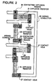
- the gauge resistors 2, 3, 4 and 5 are formed of four diffusion resistors 21, 22, 23 and 24 formed by diffusing impurities into the semiconductor beam 10.
- First and third diffusion resistors 21 and 23 are oriented in parallel to each other and in parallel to a lengthwise direction of the beam 10
- second and fourth diffusion resistors 22 and 24 are oriented in parallel to each other and in parallel to a widthwise direction of the beam 10 and perpendicularly to the lengthwise direction of the beam 10.
- the second diffusion resistor 22 is located between the first and third diffusion resistors 21 and 23, and the third diffusion resistor 23 is located between the second and fourth diffusion resistors 22 and 24.
- Each of the four diffusion resistors 21, 22, 23 and 24 has a contact diffusion region 25 formed at each end thereof.
- Each contact diffusion region 25 has an impurity diffusion concentration higher than that of the associated diffusion resistor 21, 22, 23 or 24.
- the contact diffusion region 25 formed at each end of each diffusion resistor 21, 22, 23 or 24 is connected to a wiring conductor 26 which is formed on an insulating layer (not shown) deposited to cover an upper surface of the semiconductor substrate, through a contact hole 27 which is formed through the insulating layer (not shown) so as to interconnect the contact diffusion region 25 and the wiring conductor 26.
- each connection node of the Wheatstone bridge is connected through the wiring conductor 26 to a corresponding one of the external connection pads 8 shown in Figure 1.
- the diffusion resistors 21, 22, 23 and 24 can be formed by a single diffusion process, but the contact diffusion regions 25 are formed by a plurality of diffusion processes, which may include or may not include the diffusion process forming the diffusion resistors 21, 22, 23 and 24.
- a contact resistance for each gauge resistor includes a resistance between each diffusion resistor 21, 22, 23 or 24 and the associated contact diffusion region 25, and a contact surface resistance between the associated contact diffusion region 25 and the wiring conductor 26 through the associated contact hole 27.
- a resistance of each each diffusion resistor 21, 22, 23 or 24 is R
- the contact resistance between each diffusion resistor 21, 22, 23 or 24 and the associated contact diffusion region 25 is ⁇ R 1
- the contact resistance between the associated contact diffusion region 25 and the wiring conductor 26 through the associated contact hole 27 is ⁇ R 2 .
- the contact resistance ⁇ R 1 is a mutual contacting resistance between two diffusion regions formed in the same silicon substrate, the contact resistance ⁇ R 1 becomes extremely small.
- the contact resistances ⁇ R 2 and ⁇ R 3 between the wiring conductor 26 made of a conductive material such as aluminum and the diffusion resistor or region formed in the silicon substrate 7 are in proportion to a sheet resistance of the diffusion resistor or region itself. Therefore, the contact resistance ⁇ R 2 is in proportion to the sheet resistance of the contact diffusion region 25, and the contact resistance ⁇ R 3 of the conventional semiconductor accelerometer is in proportion to the sheet resistance of the diffusion resistor itself.
- the sheet resistance of the gauge resistor 2 to 5 is about ten times as large as the sheet resistance of the contact diffusion region 25, the relation of ⁇ R 2 ⁇ ⁇ R 3 holds. Therefore, ⁇ R 1 ⁇ ⁇ R 2 ⁇ ⁇ R 3 holds.
- the contact resistance is significantly reduced, influence of a temperature coefficient can be greatly suppressed, and therefore, the offset thermal properties of the gauge resistor can be considerably improved.
- the cantilever 1 forms an acceleration response member.
- the acceleration response member is formed of a mass-spring system 30, which includes a weight or seismic mass 38 elastically supported at its opposite sides by four beams 31 to 34 extending from a frame member 39.
- the beams 31 and 32 extend from one side of the frame member 39 to one facing side of the weight 38, and the beams 33 and 34 extend from a side of the frame member 39 opposite to the side from which the beams 31 and 32 extends.
- the beams 33 and 34 reach a side of the weight 38 opposite to the side to which the beams 31 and 32 are coupled.
- two gauge resistors 35 are formed in each of the four beams 31 to 34, in such a manner that one of the two gauge resistors 35 extends along a lengthwise direction of the beam and the other of the two gauge resistors 35 extends along a widthwise direction of the beam.
- the gauge resistors formed on the beams 31 and 32 are interconnected by wiring conductors to form one Wheatstone bridge, each connection node of which is connected through a wiring conductor 36 to a corresponding one of external connection pads 37 formed on a portion of the frame member 39 adjacent to the beams 31 and 32.
- gauge resistors formed on the beams 33 and 34 are interconnected by wiring conductors to form another Wheatstone bridge, each connection node of which is connected through a wiring conductor 36 to a corresponding one of extemal connection pads 37 formed on a portion of the frame member 39 adjacent to the beams 33 and 34.
- each of the gauge resistors 35 has a diffusion resistor formed in the semiconductor beam, and one contact diffusion region which is formed at each end of the diffusion resistor and which has a diffusion concentration higher than that of the diffusion resistor.
Landscapes
- Physics & Mathematics (AREA)
- General Physics & Mathematics (AREA)
- Pressure Sensors (AREA)
Claims (4)
- Accéléromètre à semiconducteur comprenant :a) un élément de cadre semiconducteur (39) ;b) un système masse-ressort (30) comportant une masse sismique (38) supportée élastiquement au niveau de deux côtés opposés par une paire respective de poutres (31 à 34) réalisées en un matériau semiconducteur et s'étendant d'un seul tenant depuis l'élément de cadre semiconducteur (39) jusqu'à la masse sismique (38) ;c) une unique paire de résistances de jauge (35) formées dans chacune des poutres de telle sorte que l'une des résistances de jauge s'étende suivant une direction de longueur des poutres et que l'autre des résistances de jauge s'étende suivant une direction de largeur des poutres ;d) dans lequel lesdites quatre résistances de jauge (35) formées dans la première paire de poutres (31, 32) sont interconnectées par des conducteurs de câblage afin de former un premier pont de Wheatstone dont chaque noeud de connexion est connecté par l'intermédiaire d'un conducteur de câblage (36) à l'un correspondant de plots de connexion externes (37) formés sur une première partie de l'élément de cadre semiconducteur (39) adjacente à la première paire de poutres (31, 32) ;e) lesdites quatre résistances de jauge (35) formées dans la seconde paire de poutres (33, 34) sont interconnectées par des conducteurs de câblage afin de former un second pont de Wheatstone dont chaque noeud de connexion est connecté par l'intermédiaire d'un conducteur de câblage à l'un correspondant de plots de connexion externes formés sur une seconde partie de l'élément de cadre semiconducteur adjacente à la seconde paire de poutres (33, 34) ; etf) lesdites résistances de jauge (35) comprennent des résistances de diffusion et des régions de diffusion de contact, chacune desdites régions de diffusion de contact est formée au niveau de chaque extrémité des résistances de diffusion et présente une concentration de diffusion qui est supérieure à celle des résistances de diffusion.
- Accéléromètre à semiconducteur selon la revendication 1, dans lequel une première paire desdites poutres s'étendent depuis un côté de l'élément de cadre semiconducteur jusqu'à un côté faisant face de la masse sismique et une seconde paire des poutres s'étendent depuis un côté de l'élément de cadre semiconducteur opposé audit un côté de l'élément de cadre semiconducteur depuis lequel la première paire de poutres s'étendent, ladite seconde paire de poutres atteignant un côté de la masse sismique opposé au côté auquel la première paire de poutres sont couplées.
- Accéléromètre à semiconducteur selon la revendication 1 ou 2, dans lequel chacune desdites résistances de diffusion est connectée pour former un circuit série de telle sorte qu'une région de diffusion de contact d'une extrémité d'une résistance de diffusion soit connectée à une autre région de diffusion de contact d'une extrémité d'une autre résistance de diffusion.
- Accéléromètre à semiconducteur selon la revendication 3, dans lequel ladite une région de diffusion de contact de ladite une extrémité de ladite une résistance de diffusion est connectée à ladite autre région de diffusion de contact de ladite une extrémité de ladite autre résistance de diffusion par le conducteur de câblage qui comporte une première extrémité connectée par l'intermédiaire d'un trou de contact à ladite une région de diffusion de contact de ladite une extrémité de ladite une résistance de diffusion et qui comporte également une seconde extrémité connectée par l'intermédiaire d'un autre trou de contact à ladite autre région de diffusion de contact de ladite une extrémité de ladite autre résistance de diffusion.
Applications Claiming Priority (2)
| Application Number | Priority Date | Filing Date | Title |
|---|---|---|---|
| JP117088/90 | 1990-05-07 | ||
| JP2117088A JPH0413975A (ja) | 1990-05-07 | 1990-05-07 | 半導体加速度センサ |
Publications (2)
| Publication Number | Publication Date |
|---|---|
| EP0456190A1 EP0456190A1 (fr) | 1991-11-13 |
| EP0456190B1 true EP0456190B1 (fr) | 1996-08-21 |
Family
ID=14703099
Family Applications (1)
| Application Number | Title | Priority Date | Filing Date |
|---|---|---|---|
| EP91107407A Expired - Lifetime EP0456190B1 (fr) | 1990-05-07 | 1991-05-07 | Accéléromètre piézorésistif |
Country Status (4)
| Country | Link |
|---|---|
| US (1) | US5251485A (fr) |
| EP (1) | EP0456190B1 (fr) |
| JP (1) | JPH0413975A (fr) |
| DE (1) | DE69121458T2 (fr) |
Families Citing this family (16)
| Publication number | Priority date | Publication date | Assignee | Title |
|---|---|---|---|---|
| JP2831195B2 (ja) * | 1992-03-25 | 1998-12-02 | 富士電機株式会社 | 半導体加速度センサ |
| US5665915A (en) * | 1992-03-25 | 1997-09-09 | Fuji Electric Co., Ltd. | Semiconductor capacitive acceleration sensor |
| US5780742A (en) * | 1993-04-15 | 1998-07-14 | Honeywell Inc. | Mechanical resonance, silicon accelerometer |
| JPH06350105A (ja) * | 1993-06-07 | 1994-12-22 | Nec Corp | マイクロマシンとその製造方法 |
| US6467345B1 (en) | 1993-10-18 | 2002-10-22 | Xros, Inc. | Method of operating micromachined members coupled for relative rotation |
| US6426013B1 (en) | 1993-10-18 | 2002-07-30 | Xros, Inc. | Method for fabricating micromachined members coupled for relative rotation |
| US6044705A (en) * | 1993-10-18 | 2000-04-04 | Xros, Inc. | Micromachined members coupled for relative rotation by torsion bars |
| US5488862A (en) * | 1993-10-18 | 1996-02-06 | Armand P. Neukermans | Monolithic silicon rate-gyro with integrated sensors |
| JPH08211091A (ja) * | 1995-02-07 | 1996-08-20 | Mitsubishi Electric Corp | 半導体加速度検出装置 |
| JP3281217B2 (ja) * | 1995-05-23 | 2002-05-13 | 富士電機株式会社 | 半導体式加速度センサと該センサのセンサ素子の特性評価方法 |
| US5861549A (en) * | 1996-12-10 | 1999-01-19 | Xros, Inc. | Integrated Silicon profilometer and AFM head |
| US5895866A (en) * | 1996-01-22 | 1999-04-20 | Neukermans; Armand P. | Micromachined silicon micro-flow meter |
| KR100573709B1 (ko) * | 1996-04-26 | 2006-09-11 | 더 니뽄 시그널 컴파니, 리미티드 | 전자엑츄에이터및그제조방법 |
| JP4776779B2 (ja) | 1998-09-02 | 2011-09-21 | カイロス・インク | 捩り撓みヒンジで連結されて相対的に回転する微細加工部材 |
| KR100868758B1 (ko) * | 2007-01-15 | 2008-11-13 | 삼성전기주식회사 | 압저항 센서를 구비한 회전형 mems 디바이스 |
| JP5930127B2 (ja) * | 2013-06-04 | 2016-06-08 | 株式会社村田製作所 | 加速度センサ |
Family Cites Families (5)
| Publication number | Priority date | Publication date | Assignee | Title |
|---|---|---|---|---|
| US3815222A (en) * | 1971-01-06 | 1974-06-11 | Signetics Corp | Semiconductor structure and method for lowering the collector resistance |
| JPS61139758A (ja) * | 1984-12-12 | 1986-06-27 | Nissan Motor Co Ltd | 半導体加速度センサ |
| JPS62190774A (ja) * | 1986-02-18 | 1987-08-20 | Nissan Motor Co Ltd | 加速度センサ |
| JPS6341080A (ja) * | 1986-08-06 | 1988-02-22 | Nissan Motor Co Ltd | 半導体加速度センサ |
| JPH01301174A (ja) * | 1988-05-30 | 1989-12-05 | Mitsubishi Electric Corp | 半導体加速度センサ |
-
1990
- 1990-05-07 JP JP2117088A patent/JPH0413975A/ja active Pending
-
1991
- 1991-05-07 US US07/695,819 patent/US5251485A/en not_active Expired - Fee Related
- 1991-05-07 EP EP91107407A patent/EP0456190B1/fr not_active Expired - Lifetime
- 1991-05-07 DE DE69121458T patent/DE69121458T2/de not_active Expired - Fee Related
Non-Patent Citations (1)
| Title |
|---|
| Kongress Sensor 88, Vortragsmanuskripte, Band B, April 1988; ACS Organsiations GmbH; pages 265-274; Dr. Hans Reimann: "New mechanical structures to achieve low pressure silicon sensors and accelerometers" * |
Also Published As
| Publication number | Publication date |
|---|---|
| EP0456190A1 (fr) | 1991-11-13 |
| DE69121458D1 (de) | 1996-09-26 |
| DE69121458T2 (de) | 1996-12-19 |
| US5251485A (en) | 1993-10-12 |
| JPH0413975A (ja) | 1992-01-17 |
Similar Documents
| Publication | Publication Date | Title |
|---|---|---|
| EP0456190A1 (fr) | Accéléromètre piézorésistif | |
| JP3457037B2 (ja) | 集積型加速度計 | |
| EP0146709B1 (fr) | Capteur de pression | |
| US4488445A (en) | Integrated silicon accelerometer with cross-axis compensation | |
| US4553436A (en) | Silicon accelerometer | |
| US5714690A (en) | Piezoresistive silicon pressure sensor manufacture implementing long diaphragms with large aspect ratios | |
| US5239870A (en) | Semiconductor acceleration sensor with reduced cross axial sensitivity | |
| US4869107A (en) | Acceleration sensor for use in automotive vehicle | |
| US5081867A (en) | Semiconductor sensor | |
| US20040025591A1 (en) | Accleration sensor | |
| US4739381A (en) | Piezoresistive strain sensing device | |
| JPH10177033A (ja) | 加速度測定装置 | |
| KR100499970B1 (ko) | 가속도 센서 | |
| EP1643255B1 (fr) | Capteur semi-conducteur d'accélération | |
| US6763719B2 (en) | Acceleration sensor | |
| EP1868000B1 (fr) | Detecteur d acceleration | |
| EP1298442A1 (fr) | Capteur d'accélération | |
| JP3330074B2 (ja) | 3軸加速度センサ | |
| JP2551625B2 (ja) | 半導体加速度センサ | |
| JPH05281251A (ja) | 加速度センサおよびその製造方法 | |
| JP3282570B2 (ja) | 半導体加速度センサ | |
| US5212986A (en) | Semiconductor acceleration sensor including off axis acceleration cancellation | |
| JPH0648421Y2 (ja) | 半導体加速度センサ | |
| JPH08160070A (ja) | 加速度センサ | |
| EP0555727A1 (fr) | Accéléromètre à semi-conducteur |
Legal Events
| Date | Code | Title | Description |
|---|---|---|---|
| PUAI | Public reference made under article 153(3) epc to a published international application that has entered the european phase |
Free format text: ORIGINAL CODE: 0009012 |
|
| 17P | Request for examination filed |
Effective date: 19910528 |
|
| AK | Designated contracting states |
Kind code of ref document: A1 Designated state(s): DE FR GB |
|
| 17Q | First examination report despatched |
Effective date: 19931208 |
|
| GRAH | Despatch of communication of intention to grant a patent |
Free format text: ORIGINAL CODE: EPIDOS IGRA |
|
| GRAA | (expected) grant |
Free format text: ORIGINAL CODE: 0009210 |
|
| AK | Designated contracting states |
Kind code of ref document: B1 Designated state(s): DE FR GB |
|
| REF | Corresponds to: |
Ref document number: 69121458 Country of ref document: DE Date of ref document: 19960926 |
|
| ET | Fr: translation filed | ||
| PG25 | Lapsed in a contracting state [announced via postgrant information from national office to epo] |
Ref country code: GB Effective date: 19970507 |
|
| PLBE | No opposition filed within time limit |
Free format text: ORIGINAL CODE: 0009261 |
|
| STAA | Information on the status of an ep patent application or granted ep patent |
Free format text: STATUS: NO OPPOSITION FILED WITHIN TIME LIMIT |
|
| 26N | No opposition filed | ||
| GBPC | Gb: european patent ceased through non-payment of renewal fee |
Effective date: 19970507 |
|
| PG25 | Lapsed in a contracting state [announced via postgrant information from national office to epo] |
Ref country code: FR Free format text: LAPSE BECAUSE OF NON-PAYMENT OF DUE FEES Effective date: 19980130 |
|
| PG25 | Lapsed in a contracting state [announced via postgrant information from national office to epo] |
Ref country code: DE Free format text: LAPSE BECAUSE OF NON-PAYMENT OF DUE FEES Effective date: 19980203 |
|
| REG | Reference to a national code |
Ref country code: FR Ref legal event code: ST |