EP0456370A2 - Method and apparatus for controlling the diameter of a silicon single crystal - Google Patents
Method and apparatus for controlling the diameter of a silicon single crystal Download PDFInfo
- Publication number
- EP0456370A2 EP0456370A2 EP91303575A EP91303575A EP0456370A2 EP 0456370 A2 EP0456370 A2 EP 0456370A2 EP 91303575 A EP91303575 A EP 91303575A EP 91303575 A EP91303575 A EP 91303575A EP 0456370 A2 EP0456370 A2 EP 0456370A2
- Authority
- EP
- European Patent Office
- Prior art keywords
- single crystal
- diameter
- pull rate
- silicon single
- crystal
- Prior art date
- Legal status (The legal status is an assumption and is not a legal conclusion. Google has not performed a legal analysis and makes no representation as to the accuracy of the status listed.)
- Withdrawn
Links
Images



Classifications
-
- G—PHYSICS
- G01—MEASURING; TESTING
- G01B—MEASURING LENGTH, THICKNESS OR SIMILAR LINEAR DIMENSIONS; MEASURING ANGLES; MEASURING AREAS; MEASURING IRREGULARITIES OF SURFACES OR CONTOURS
- G01B11/00—Measuring arrangements characterised by the use of optical techniques
- G01B11/08—Measuring arrangements characterised by the use of optical techniques for measuring diameters
-
- C—CHEMISTRY; METALLURGY
- C30—CRYSTAL GROWTH
- C30B—SINGLE-CRYSTAL GROWTH; UNIDIRECTIONAL SOLIDIFICATION OF EUTECTIC MATERIAL OR UNIDIRECTIONAL DEMIXING OF EUTECTOID MATERIAL; REFINING BY ZONE-MELTING OF MATERIAL; PRODUCTION OF A HOMOGENEOUS POLYCRYSTALLINE MATERIAL WITH DEFINED STRUCTURE; SINGLE CRYSTALS OR HOMOGENEOUS POLYCRYSTALLINE MATERIAL WITH DEFINED STRUCTURE; AFTER-TREATMENT OF SINGLE CRYSTALS OR A HOMOGENEOUS POLYCRYSTALLINE MATERIAL WITH DEFINED STRUCTURE; APPARATUS THEREFOR
- C30B15/00—Single-crystal growth by pulling from a melt, e.g. Czochralski method
-
- Y—GENERAL TAGGING OF NEW TECHNOLOGICAL DEVELOPMENTS; GENERAL TAGGING OF CROSS-SECTIONAL TECHNOLOGIES SPANNING OVER SEVERAL SECTIONS OF THE IPC; TECHNICAL SUBJECTS COVERED BY FORMER USPC CROSS-REFERENCE ART COLLECTIONS [XRACs] AND DIGESTS
- Y10—TECHNICAL SUBJECTS COVERED BY FORMER USPC
- Y10T—TECHNICAL SUBJECTS COVERED BY FORMER US CLASSIFICATION
- Y10T117/00—Single-crystal, oriented-crystal, and epitaxy growth processes; non-coating apparatus therefor
- Y10T117/10—Apparatus
- Y10T117/1004—Apparatus with means for measuring, testing, or sensing
- Y10T117/1008—Apparatus with means for measuring, testing, or sensing with responsive control means
Definitions
- the present invention relates to a method and apparatus for controlling the diameter of a silicon single crystal and more particularly to a silicon single crytal diameter controlling method and apparatus whereby in the continuous manufacture of a silicon single crystal while rotating it relative to a crucible, the diameter of the pulled single crystal is controlled during the pulling of the crystal.
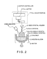
- Fig. 2 of the accompanying drawings there is illustrated a schematic diagram showing a single crystal manufacturing apparatus according to the Czochralski method which is well known as a manufacturing method of single crystals of such semiconductor as silicon. It is to be noted that the Czochralski method is widely called as the CZ method and also it is generally referred to as a crystal pulling method.
- molten silicon 3 which is heated and melted by a heater 4 so that while rotating a silicon single crystal 1 in a direction opposite to the direction of rotation of the crucible 2 by a turning mechanism which is not shown, the silicon single crystal 1 is gradually pulled by a pulling apparatus 7 and the crystal is grown in the interfacial region between the molten silicon 3 and the silicon single crystal 1.
- This silicon single crystal 1 is grown from a seed crystal 1a by crystal growth and the seed crystal 1a is supported by a seed crystal holder 9 connected to the pulling apparatus 7.
- this silicon single crystal under growth is referred to as a pulled single crystal.
- the pulling apparatus 7 includes mechanisms for respectively moving vertically and rotating the silicon single crystal 1 and it is composed of a motor controller 8, a pull motor 9, etc.
- a motor controller 8 a pull motor 9 etc.
- the crucible 2 is supported by a lifting mechanism which is not shown in addition to the previously mentioned turning mechanism and it is designed so that even if a crystal is grown, for example, the liquid level is prevented from lowering but maintained constant by the lifting mechanism and the temperature distribution in the vicinity of the liquid surface is not varied.
- the pulled single crystal 1 manufactured by the CZ method is processed into a cylindrical silicon single crystal ingot later on, it is required that the pulled single crystal 1 is pulled in such a manner that its diameter is substantially the same throughout the body portion on the whole.
- a diameter control is effected such that the diameter of the pulled single crystal 1 is directly measured during its pulling by such optical means as a video measure 5 and the pulled single crystal 1 is pulled while adjusting the pull rate in a manner that the diameter is maintained at the desired value.
- the optical means is attached to the crystal pulling apparatus so that the fusion ring appealing at the boundary of the pulled single crystal 1 and the liquid surface is measured obliquely from above with a single measuring line and the diameter of the pulled single crystal 1 is measuring directly.
- the above-mentioned diameter control of a pulled single crystal through the adjustment of the pull rate is performed by comparing the actual measured diameter value from the optical means and the desired diameter value so that the resulting deviation is subjected to the well known PID control to calculate a pull rate as a manipulated variable and this manipulated variable is applied as a command to the motor controller 8, thereby controlling the pull rate.
- the pull rate of the crystal pulling apparatus is changed, the response of the silicon single crystal or the change of the diameter of the pulled single crystal is such that a considerable time is required before its effect is exerted (the dead time is long) and also the rate of change is small (the change or response speed is low).
- the measured diameter value is compared with the desired diameter value to effect the PID control, a timely manipulation of the pull rate is required in order to accurately grasp a change in the diameter of the pulled single crystal and therefore an advanced control giving emphasis to the derivative term (derivative action) is required.
- the present invention has been made with a view to overcoming the foregoing problems in the prior art, and it is the primary object of the present invention to provide a silicon single crystal diameter control method and apparatus so designed that the algorithm of the PID processing performed in a diameter control is improved and also a dead time compensation control is added, thereby ensuring an improved desired value follow-up and eliminating any PID parameter adjusting operation of the spot.
- a silicon single crystal diameter control method so designed that in the course of manufacturing a silicon single crystal by pulling the silicon single crystal while rotating it relative to a crucible, a comparison between the measured diameter value of a pulled single crystal measured by optical means and the desired diameter value is made to determine a deviation so that the resulting deviation is subjected to incomplete differential PID processing to calculate a pull rate and the pull rate is applied to the motor controller of a crystal pulling apparatus, thereby controlling the diameter of the pulled single crystal through the manipulation of the pull rate.
- a silicon single crystal diameter control apparatus including an input unit for receiving the measured diameter value of a pulled single crystal measured by optical means, an incomplete differential PID computing unit for making a comparison between the measured diameter value of the pulled single crystal and the desired diameter value to calculate a pull rate, and an output unit for applying the pull rate to the motor controller of a crystal pulling apparatus.
- a silicon single crystal model parameterization method in which the response characteristic of the diameter value of a pulled single crystal to the pull rate is modeled by the transfer function given by the following equation and the two model parameters in the transfer function or the response speed V and the dead time L are determined by a step response test for studying the response of the diameter value when the pull rate is varied in a stepwise manner:
- Transfer function: Gp(s) V S2 ⁇ e -Ls
- a PID parameterization method which determines the optimum parameters by performing a computer simulation by using the previously mentioned silicon single crystal model.
- the incomplete differential PID control is not used alone and the diameter control according to the Smith method is performed so that in addition to the actions of the first diameter control method and apparatus, a dead time compensation model in the form of G p (s) ⁇ (1-e -Ls ) is inserted in a minor loop so that a transfer function G p (s) involving no dead time is made a control system and the diameter control excellent in desired value follow-up performance is effected.
- Fig. 1 is a schematic diagram showing the construction of an embodiment of a diameter control apparatus which is used for performing a silicon single crystal diameter control method by incomplete differential PID processing according to the present invention.
- Fig. 2 is a schematic diagram showing the construction of a conventional silicon single crystal manufacturing apparatus in accordance with the Czochralski method.
- Fig. 3 is a block diagram for explaining the function of the embodiment apparatus of Fig. 1.
- Fig. 4 is a comparative waveform diagram showing the response characteristic of the incomplete differential to the stepwise variation of the deviation.
- Fig. 5 is a schematic diagram showing the measured diameter values of a manufactured silicon single crystal.
- Fig. 6 is a schematic diagram showing the construction of an embodiment of a diameter control apparatus which is used for performing a diameter control method by the Smith method processing.
- Fig. 7 is a block diagram for explaining the function of the embodiment apparatus of Fig. 6.
- Fig. 8 is a graph showing the results of the determination by a computer simulation of the mode of the diameter control according to the Smith method.
- Embodiment 1 mainly explains a silicon single crystal diameter cpontrol method and apparatus by incomplete processing and the description of Embodiment 2 explains a diameter control method and apparatus by the Smith method processing.
- Fig. 1 is a schematic diagram showing the construction of the embodiment of the diameter control apparatus used for performing the diameter control method by incomplete differential PID processing.
- numerals 1 to 9 designate component parts which are identical equivalent to those designated by the same reference numerals used in the description of the conventional silicon single crystal manufacturing apparatus of Fig.2 and will not be described.
- Fig. 3 is a block diagram for explaining the function of the diameter control apparatus of Fig. 1.
- numeral 20 designates the portion shown in block diagram form the diameter control apparatus by incomplete differential PID processing.
- the controlled system data basically represents the measured diameter values measured by a video measure 5 used as optical means.
- the diameter control apparatus is composed of a crystal diameter input unit 10 for processing the measured diameter values, an incomplete differential PID computing unit 11 for comparing the processed measured diameter values and the desired diameter to calculate a pull rate, and a pull rate output unit 12 for applying the pull rate as a command to the silicon single crystal manufacturing apparatus (crystal pulling apparatus).
- Numeral 13 designates PID parameter unit for storing the parameters used during the processing.
- the embodiment of the diameter control method by incomplete differential PID will now described with reference to Fig. 1 and 2.
- the measured diameter values produced from the video measure 5 (these are the output of the silicon single crystal manufacturing apparatus 30 in Fig. 3 and the output of the crystal diameter input unit 10 in Fig. 1) are compared with the desired diameter stored in a memory (not shown) at a summing point 31 and a PID processing 11a utilizing an incomplete differential is performed in the incomplete differential PID computing unit 11, thereby calculating a manipulated output or a pull rate.
- This pull rate is applied to the motor controller 8 through the pull rate output unit 12 to command it and the pulled single crystal 1 is pulled at the controlled pull rate, thereby manufacturing the silicon single crystal 1.
- This control operation is performed for example several times for every rotation of the pulled singloe crystal 1 and thus this operation is performed throughout the pulling of the body portion.
- the PID parameter unit 13 stores the best parameters determined by the computer simulation using the silicon single crystal model and therefore no adjustment of the PID parameters on the spot is required.
- the manipulated output Go(s) produced by the oridnary PID action alone is given by the following equation (II) with E(s) representing the deviation between the measured diameter value and the desired diameter: where K is a proportional gain, Ti an integral time, Td a derivative time, and s a Laplace variable (complex number).
- 1/ ⁇ is called as a differential gain. While the difference between equations (II) and (III) resides in the calculation of the manipulated variable by the differentiation term, in the case of equation (III) the ordinary differentiation term output Td s of equation (II) is passed through the first-order delay filter.
- Fig. 4 shows comparative waveform diagrams of the response characteristics with respect to the stepwise variation of the deviation E(s).
- Fig. 4(a) shows the values of the deviation with respect to the time on the abscissa, and in Fig. 4(b) the ordinate represents the manipulated output variable M of the ordinary PID processing with respect to the deviation.
- Fig. 4 shows comparative waveform diagrams of the response characteristics with respect to the stepwise variation of the deviation E(s).
- Fig. 4(a) shows the values of the deviation with respect to the time on the abscissa
- Fig. 4(b) the ordinate represents the manipulated output variable M of the ordinary PID processing with respect to the deviation.
- FIG. 4(c) shows the response characteristic of the manipulated output variable M in the derivative control action portion of the incomplete differential PID processing.
- the output with respect to noise deviation is reduced by the gain of 1/ ⁇ (M/ ⁇ in the Figure) so that the sensitive response to noise is decreased and an effective differential effect is obtained.
- the silicon single crystal model used in the computer simulation for determining the PID parameters 13 it is approximated by the quadratic integral system which is given by the following equation (IV) giving consideration to the dead time L and which is capable of faithfully reproducing the actual response.
- the model parameters including the dead time L and the response speed are determined by the following procedure. Firstly, in the silicon single crystal manufacturing apparatus the pull rate is varied in a stepwise manner and the resulting response data of the silicon single crystal diameter are gathered. Then, the dead time L and the response speed V are assumed and the step response test is reproduced by a computer simulation. Then, the values of V and L are determined in such a manner that the error between the simulation result and the actual response waveform data is reduced to a minimum.
- FIG. 5 shows the results of the diameter measurements made at the positions of 0.0, 50.0, 100.0, 150.0, 200.0 and 250.0 mm from the top of the effective body portion of the manufactured silicon single crystal. As shown in Fig. 5, the maximum and minimum values of the deviation from the desired diameter of 160.0mm were less than + 0.5mm and the manufactured silicon single crystal was uniform in diameter at the various portions.
- this data represents the first manufacture made on the basis of the PID parameters determined by the computer simulation using the silicon single crystal model and the silicon single crystal accurately following the desired diameter in this way was manufactured at the first attempt.
- FIG. 6 there is illustrated a schematic diagram showing the construction of an embodiment of a diameter control apparatus used for performing a diameter control method according to the Smith method processing.
- FIG. 7 is a block diagram for explaining the function of the diameter control apparatus of Fig. 6.
- numeral 21 designates the portion showing in block diagram form the diameter control apparatus by the Smith method processing
- numeral 14 designates a Smith method computing unit. While this embodiment is identical in construction with the embodiment of Fig. 1 except that the incomplete differential PID computing unit 11 is replaced by the Smith method computing unit 14, as will be seen from Fig. 7, though the principal adjusting function of the Smith method control is the operation of the incomplete differential PID 11a, the diameter control of a pulled single crystal 1 according to the Smith method has an additional feature that the silicon single crystal model given by equation (IV) is used for the determination of a control deviation.
- Fig. 8 is a graph showing the result by a computer simulation of the model of the diameter control according to the Smith method control in the manufacture of a silicon single crystal.
- the abscissa represents the control time and the ordinate represents the pulled single crystal diameter.
- the solid line indicates the control characteristic according to the Smith method and the simulation result according to the conventional PID control is indicated by the broken line for reference purposes.
- the control characteristic was determined by using the initial diameter of 162.0mm and the desired diameter of 160.0mm.
- the PID control requires about 2 hours until the measured diameter becomes equal to the desired diameter, whereas the Smith method requires about 1 hour and the Smith method ensures a dead time-compensated control which is excellent in desired value follow-up.
Landscapes
- Physics & Mathematics (AREA)
- General Physics & Mathematics (AREA)
- Chemical & Material Sciences (AREA)
- Engineering & Computer Science (AREA)
- Crystallography & Structural Chemistry (AREA)
- Materials Engineering (AREA)
- Metallurgy (AREA)
- Organic Chemistry (AREA)
- Crystals, And After-Treatments Of Crystals (AREA)
Abstract
A method of controlling the diameter of a silicon single crystal. In the course of manufacturing a silicon single crystal (1) by pulling the silicon single crystal while rotating it relative to a crucible (2), a comparison between a measured diameter value of the pulled single crystal measured by optical means (5) and a desired diameter value is made to determine a deviation so that the resulting deviation is subjected to an incomplete difference PID processing or the Smith method processing to calculate (11) a pull rate and the pull rate is applied to a motor controller (8) of a crystal pulling apparatus (7) thereby performing the diameter control of the pulled single crystal through the manipulation of the pull rate. An apparatus for controlling the diameter of a silicon single crystal includes input means for receiving a measured diameter value of a pulled single crystal measured by optical means, incomplete differential PID computing means (11) for making a comparison between a measured diameter value of the pulled single crystal and a desired diameter value a plurality of times at intervals of a unit rotational period to calculate a pull rate, and output means (12) for applying the pull rate to a motor controller (8) of a crystal pulling apparatus (7).
Description
- The present invention relates to a method and apparatus for controlling the diameter of a silicon single crystal and more particularly to a silicon single crytal diameter controlling method and apparatus whereby in the continuous manufacture of a silicon single crystal while rotating it relative to a crucible, the diameter of the pulled single crystal is controlled during the pulling of the crystal.
- Referring to Fig. 2 of the accompanying drawings, there is illustrated a schematic diagram showing a single crystal manufacturing apparatus according to the Czochralski method which is well known as a manufacturing method of single crystals of such semiconductor as silicon. It is to be noted that the Czochralski method is widely called as the CZ method and also it is generally referred to as a crystal pulling method.
- In the Figure, during the manufacture of a silicon single crystal, contained in a
crucible 2 ismolten silicon 3 which is heated and melted by aheater 4 so that while rotating a siliconsingle crystal 1 in a direction opposite to the direction of rotation of thecrucible 2 by a turning mechanism which is not shown, the siliconsingle crystal 1 is gradually pulled by apulling apparatus 7 and the crystal is grown in the interfacial region between themolten silicon 3 and the siliconsingle crystal 1. This siliconsingle crystal 1 is grown from aseed crystal 1a by crystal growth and theseed crystal 1a is supported by aseed crystal holder 9 connected to thepulling apparatus 7. In the description to follow, this silicon single crystal under growth is referred to as a pulled single crystal. Also, the pullingapparatus 7 includes mechanisms for respectively moving vertically and rotating the siliconsingle crystal 1 and it is composed of amotor controller 8, apull motor 9, etc. Thus, it is a well known apparatus and any detailed explanation of its construction will be omitted. Thecrucible 2 is supported by a lifting mechanism which is not shown in addition to the previously mentioned turning mechanism and it is designed so that even if a crystal is grown, for example, the liquid level is prevented from lowering but maintained constant by the lifting mechanism and the temperature distribution in the vicinity of the liquid surface is not varied. - Since the pulled
single crystal 1 manufactured by the CZ method is processed into a cylindrical silicon single crystal ingot later on, it is required that the pulledsingle crystal 1 is pulled in such a manner that its diameter is substantially the same throughout the body portion on the whole. For this purpose, a diameter control is effected such that the diameter of the pulledsingle crystal 1 is directly measured during its pulling by such optical means as avideo measure 5 and the pulledsingle crystal 1 is pulled while adjusting the pull rate in a manner that the diameter is maintained at the desired value. In this case, the optical means is attached to the crystal pulling apparatus so that the fusion ring appealing at the boundary of the pulledsingle crystal 1 and the liquid surface is measured obliquely from above with a single measuring line and the diameter of the pulledsingle crystal 1 is measuring directly. - The above-mentioned diameter control of a pulled single crystal through the adjustment of the pull rate is performed by comparing the actual measured diameter value from the optical means and the desired diameter value so that the resulting deviation is subjected to the well known PID control to calculate a pull rate as a manipulated variable and this manipulated variable is applied as a command to the
motor controller 8, thereby controlling the pull rate. - With the above-mentioned silicon single crystal diameter control method and apparatus described above, it is general that if, for example, the pull rate of the crystal pulling apparatus is changed, the response of the silicon single crystal or the change of the diameter of the pulled single crystal is such that a considerable time is required before its effect is exerted (the dead time is long) and also the rate of change is small (the change or response speed is low). Thus, where the measured diameter value is compared with the desired diameter value to effect the PID control, a timely manipulation of the pull rate is required in order to accurately grasp a change in the diameter of the pulled single crystal and therefore an advanced control giving emphasis to the derivative term (derivative action) is required. However, considerable noise is included in the measured diameter value of the pulled single crystal measured by the optical means and there is the danger of the pull speed being varied excessively under the effect of such noise, Thus making it impossible to effect a control emphasizing the derivative term. Thus, there is a limit to the control of the crystal diameter variation and the yield of the crystal tends to deteriorate.
- In addition, the adjustment of the PID parameters on the spot is essential and thus it is necessary to wastefully pull the silicon single crystal for the purpose of PID parameter adjustment alone.
- The present invention has been made with a view to overcoming the foregoing problems in the prior art, and it is the primary object of the present invention to provide a silicon single crystal diameter control method and apparatus so designed that the algorithm of the PID processing performed in a diameter control is improved and also a dead time compensation control is added, thereby ensuring an improved desired value follow-up and eliminating any PID parameter adjusting operation of the spot.
- To accomplish the above object, in accordance with one aspect of the present invention there is thus provided a silicon single crystal diameter control method so designed that in the course of manufacturing a silicon single crystal by pulling the silicon single crystal while rotating it relative to a crucible, a comparison between the measured diameter value of a pulled single crystal measured by optical means and the desired diameter value is made to determine a deviation so that the resulting deviation is subjected to incomplete differential PID processing to calculate a pull rate and the pull rate is applied to the motor controller of a crystal pulling apparatus, thereby controlling the diameter of the pulled single crystal through the manipulation of the pull rate.
- In accordance with another aspect of the present invention there is provided such silicon single crystal diameter control method in which the incomplete differential PID processing is replaced with the processing by the Smith method to calculate a pull rate.
- In accordance with still another aspect of the present invention, there is provided a silicon single crystal diameter control apparatus including an input unit for receiving the measured diameter value of a pulled single crystal measured by optical means, an incomplete differential PID computing unit for making a comparison between the measured diameter value of the pulled single crystal and the desired diameter value to calculate a pull rate, and an output unit for applying the pull rate to the motor controller of a crystal pulling apparatus.
- In accordance with still another aspect of the present invention there is provided such silicon single crystal diameter controlling apparatus in which the incomplete differential PID computing unit is replaced with a Smith method computing unit.
- In accordance with still another aspect of the present invention there is provided a silicon single crystal model parameterization method in which the response characteristic of the diameter value of a pulled single crystal to the pull rate is modeled by the transfer function given by the following equation and the two model parameters in the transfer function or the response speed V and the dead time L are determined by a step response test for studying the response of the diameter value when the pull rate is varied in a stepwise manner:

- In accordance with still another aspect of the present invention there is provided a PID parameterization method which determines the optimum parameters by performing a computer simulation by using the previously mentioned silicon single crystal model.
- In accordance with the first silicon single crystal diameter control method and apparatus there is exhibited an effective differential effect in which the effect of noise in the measured diameter values is reduced by the incomplete differential PID control, thereby causing the diameter value of the silicon single crystal to become extremely close to the desired value.
- Also, in accordance with the second silicon single crystal diameter control method and apparatus, the incomplete differential PID control is not used alone and the diameter control according to the Smith method is performed so that in addition to the actions of the first diameter control method and apparatus, a dead time compensation model in the form of Gp(s)·(1-e-Ls) is inserted in a minor loop so that a transfer function Gp(s) involving no dead time is made a control system and the diameter control excellent in desired value follow-up performance is effected.
- It is to be noted that the PID parameters and the Smith parameters, which are applied to the computing means of the above-mentioned diameter control method and apparatus, are not determined by actually pulling silicon single crystals and the optimum parameters are determined by computer simulations.
- Fig. 1 is a schematic diagram showing the construction of an embodiment of a diameter control apparatus which is used for performing a silicon single crystal diameter control method by incomplete differential PID processing according to the present invention.
- Fig. 2 is a schematic diagram showing the construction of a conventional silicon single crystal manufacturing apparatus in accordance with the Czochralski method.
- Fig. 3 is a block diagram for explaining the function of the embodiment apparatus of Fig. 1.
- Fig. 4 is a comparative waveform diagram showing the response characteristic of the incomplete differential to the stepwise variation of the deviation.
- Fig. 5 is a schematic diagram showing the measured diameter values of a manufactured silicon single crystal.
- Fig. 6 is a schematic diagram showing the construction of an embodiment of a diameter control apparatus which is used for performing a diameter control method by the Smith method processing.
- Fig. 7 is a block diagram for explaining the function of the embodiment apparatus of Fig. 6.
- Fig. 8 is a graph showing the results of the determination by a computer simulation of the mode of the diameter control according to the Smith method.
- Preferred embodiments of the present invention will now be described. The description of Embodiment 1 mainly explains a silicon single crystal diameter cpontrol method and apparatus by incomplete processing and the description of Embodiment 2 explains a diameter control method and apparatus by the Smith method processing.
- Fig. 1 is a schematic diagram showing the construction of the embodiment of the diameter control apparatus used for performing the diameter control method by incomplete differential PID processing. In the Figure,
numerals 1 to 9 designate component parts which are identical equivalent to those designated by the same reference numerals used in the description of the conventional silicon single crystal manufacturing apparatus of Fig.2 and will not be described. Fig. 3 is a block diagram for explaining the function of the diameter control apparatus of Fig. 1. - In Fig. 1,
numeral 20 designates the portion shown in block diagram form the diameter control apparatus by incomplete differential PID processing. In this apparatus, the controlled system data basically represents the measured diameter values measured by avideo measure 5 used as optical means. As shown in the Figure, the diameter control apparatus is composed of a crystaldiameter input unit 10 for processing the measured diameter values, an incomplete differentialPID computing unit 11 for comparing the processed measured diameter values and the desired diameter to calculate a pull rate, and a pullrate output unit 12 for applying the pull rate as a command to the silicon single crystal manufacturing apparatus (crystal pulling apparatus). Numeral 13 designates PID parameter unit for storing the parameters used during the processing. - The embodiment of the diameter control method by incomplete differential PID will now described with reference to Fig. 1 and 2. The measured diameter values produced from the video measure 5 (these are the output of the silicon single
crystal manufacturing apparatus 30 in Fig. 3 and the output of the crystaldiameter input unit 10 in Fig. 1) are compared with the desired diameter stored in a memory (not shown) at asumming point 31 and aPID processing 11a utilizing an incomplete differential is performed in the incomplete differentialPID computing unit 11, thereby calculating a manipulated output or a pull rate. This pull rate is applied to themotor controller 8 through the pullrate output unit 12 to command it and the pulledsingle crystal 1 is pulled at the controlled pull rate, thereby manufacturing the siliconsingle crystal 1. This control operation is performed for example several times for every rotation of the pulledsingloe crystal 1 and thus this operation is performed throughout the pulling of the body portion. - By performing the foregoing diameter control method, it is possible to manufacture a silicon
single crystal 1 which is reduced in diameter variation and which is close in diameter value to the desired diameter. It is to be noted that in this control method thePID parameter unit 13 stores the best parameters determined by the computer simulation using the silicon single crystal model and therefore no adjustment of the PID parameters on the spot is required. - The algorithm of the incomplete differential PID processing and the model parameterization method will now be described.
- The manipulated output Go(s) produced by the oridnary PID action alone is given by the following equation (II) with E(s) representing the deviation between the measured diameter value and the desired diameter:

- On the other hand, the following equation (III) gives the manipulated output G(s) of the incomlete differential PID action used in the diameter control of the present invention.

- Here, 1/α is called as a differential gain. While the difference between equations (II) and (III) resides in the calculation of the manipulated variable by the differentiation term, in the case of equation (III) the ordinary differentiation term output Td s of equation (II) is passed through the first-order delay filter. Fig. 4 shows comparative waveform diagrams of the response characteristics with respect to the stepwise variation of the deviation E(s). Fig. 4(a) shows the values of the deviation with respect to the time on the abscissa, and in Fig. 4(b) the ordinate represents the manipulated output variable M of the ordinary PID processing with respect to the deviation. Fig. 4(c) shows the response characteristic of the manipulated output variable M in the derivative control action portion of the incomplete differential PID processing. As will be seen from Fig. 4, in the case of the incomplete differential PID, as for example, the output with respect to noise deviation is reduced by the gain of 1/α(M/α in the Figure) so that the sensitive response to noise is decreased and an effective differential effect is obtained.
- Also, as regards the silicon single crystal model used in the computer simulation for determining the
PID parameters 13, it is approximated by the quadratic integral system which is given by the following equation (IV) giving consideration to the dead time L and which is capable of faithfully reproducing the actual response.
The model parameters including the dead time L and the response speed are determined by the following procedure. Firstly, in the silicon single crystal manufacturing apparatus the pull rate is varied in a stepwise manner and the resulting response data of the silicon single crystal diameter are gathered. Then, the dead time L and the response speed V are assumed and the step response test is reproduced by a computer simulation. Then, the values of V and L are determined in such a manner that the error between the simulation result and the actual response waveform data is reduced to a minimum. - A description will now be made of the results of a working example in which a silicon single crystal was actually manufactured by the above-mentioned incomplete differential PID control method and apparatus.
- In this working example, a series of operations including the comparison between the moving average value of measured diameter data every 0.1 sec. and a desired diameter value, the calculation of a pull rate and the application of the pull rate to the
motor controller 8 were performed once every second, that is, the operations were performed 3 times for even rotation of the silicon single crystal. (The rotational speed of the pulled single crystal was 20.0 rpm). As regards controlling cycle, when pull rate and rotations increases and the same time a disturbance caused by operation, such as temperature variations etc. in crucible increases, further shortening thereof is effectuated on the diameter control of a pulled single crystal. The desired diameter of the body portion was 160.0 mm. The schematic diagram of Fig. 5 shows the results of the diameter measurements made at the positions of 0.0, 50.0, 100.0, 150.0, 200.0 and 250.0 mm from the top of the effective body portion of the manufactured silicon single crystal. As shown in Fig. 5, the maximum and minimum values of the deviation from the desired diameter of 160.0mm were less than + 0.5mm and the manufactured silicon single crystal was uniform in diameter at the various portions. - Also, this data represents the first manufacture made on the basis of the PID parameters determined by the computer simulation using the silicon single crystal model and the silicon single crystal accurately following the desired diameter in this way was manufactured at the first attempt.
- Referring to Fig. 6, there is illustrated a schematic diagram showing the construction of an embodiment of a diameter control apparatus used for performing a diameter control method according to the Smith method processing.
- In the Figure,
numerals 1 to 13 excluding 11 designate component parts which are identical or equivalent to those designated by the same reference numerals used in the description of the embodiment apparatus of Fig. 1. Fig. 7 is a block diagram for explaining the function of the diameter control apparatus of Fig. 6. - In Fig. 6, numeral 21 designates the portion showing in block diagram form the diameter control apparatus by the Smith method processing, and numeral 14 designates a Smith method computing unit. While this embodiment is identical in construction with the embodiment of Fig. 1 except that the incomplete differential
PID computing unit 11 is replaced by the Smithmethod computing unit 14, as will be seen from Fig. 7, though the principal adjusting function of the Smith method control is the operation of the incompletedifferential PID 11a, the diameter control of a pulledsingle crystal 1 according to the Smith method has an additional feature that the silicon single crystal model given by equation (IV) is used for the determination of a control deviation. In other words, in addition to the principal loop of the feedback to the incompletedifferential PID 11a, a transfer function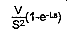
point 2, thereby determining a control deviation. In this way, the dead time-compensated control is made possible thus accomplishing the diameter control which is excellent in desired value follow-up performance. - Fig. 8 is a graph showing the result by a computer simulation of the model of the diameter control according to the Smith method control in the manufacture of a silicon single crystal. In the Figure, the abscissa represents the control time and the ordinate represents the pulled single crystal diameter. The solid line indicates the control characteristic according to the Smith method and the simulation result according to the conventional PID control is indicated by the broken line for reference purposes. In the case of the simulation, the control characteristic was determined by using the initial diameter of 162.0mm and the desired diameter of 160.0mm. As will be seen from the Figure, the PID control requires about 2 hours until the measured diameter becomes equal to the desired diameter, whereas the Smith method requires about 1 hour and the Smith method ensures a dead time-compensated control which is excellent in desired value follow-up.
- From the foregoing it will be seen that in accordance with the silicon single crystal diameter control method and apparatus of the present invention there is an effect that not only the diameter control capable of reducing the effect of noise during the pulling of a single crystal is ensured by the incomplete differential PID control thus improving the control performance and thereby ensuring the uniformity of crystal quality, but also the control which gives emphasis to the differential term is ensured thus making the diameter extremely close to the desired value and thereby ensuring the improved yield.
- Also, in accordance with the control using the Smith method, not only the effect due to the same action as the incomplete differential PID control is obtained but also the dead time-compensated control is ensured, thus accomplishing the diameter control which is excellent in desired value follow-up performance and thereby further improving the yield.
- Further, since the manufacture of a silicon single crystal using the best PID parameters determined by the computer simulation is ensured from the start, it is possible to eliminate any redundant operations encountered in the manufacture of silicon single crystals by the conventional methods such as the useless pulling of a crystal, that is, the actual pulling of a silicon single crystal for the determination of parameters.
Claims (6)
- A silicon single crystal diameter control method for controlling a diameter of a pulled single crystal rotated relative to a crucible in accordance with a crystal pull rate, said method comprising the steps of:
making a comparison between a measured diameter value of said pulled single crystal measured by optical means and a desired diameter value to determine a deviation;
subjecting said deviation to an incomplete differential PID processing to calculate a single crystal pull rate; and
applying said single crystal pull rate as a command to pull means to control the diameter of said pulled single crystal at a desired diameter. - A silicon single crystal diameter control method according to claim 1, wherein said deviation is processed by the Smith method in place of said incomplete differential PID processing.
- A silicon single crystal diameter control apparatus for controlling a diameter of a pulled single crystal rotated relative to a crucible in accordance with a crystal pull rate, said apparatus comprising:
crystal diameter input means for receiving a measured diameter value of said pulled single crystal measured by optical means;
incomplete differential PID computing means for making a comparison between a measured diameter value and a desired diameter value to calculate a pull rate of said single crystal from a resulting deviation; and
pull rate output means for applying said crystal pull rate as a command to pull means. - A silicon single crystal diameter control apparatus according to claim 3, wherein Smith method computing means is used in place of said incomplete differential PID computing means.
- A model parameterization method comprising the steps of:
defining a response characteristic of a diameter value of a pulled single crystal to a crystal pull rate in accordance with a transfer function given by the following equation (I); and
performing a step response test for determining a response of said measured diameter value to a stepwise variation of said crystal pull rate to determine two model parameters of V and L in said transfer function:
V = response speed
L = dead time
S = Laplace variable - A PID parameterization method wherein PID parameters used in the calculations of said incomplete differential PID processing stated in claims 1 and 3 and the Smith method parameters used in the calculations of said Smith method processing stated in claims 2 and 4 are respectively determined by a computer simulation using said silicon single crystal model stated in claim 5.
Applications Claiming Priority (2)
| Application Number | Priority Date | Filing Date | Title |
|---|---|---|---|
| JP110385/90 | 1990-04-27 | ||
| JP11038590 | 1990-04-27 |
Publications (2)
| Publication Number | Publication Date |
|---|---|
| EP0456370A2 true EP0456370A2 (en) | 1991-11-13 |
| EP0456370A3 EP0456370A3 (en) | 1992-08-12 |
Family
ID=14534468
Family Applications (1)
| Application Number | Title | Priority Date | Filing Date |
|---|---|---|---|
| EP19910303575 Withdrawn EP0456370A3 (en) | 1990-04-27 | 1991-04-22 | Method and apparatus for controlling the diameter of a silicon single crystal |
Country Status (5)
| Country | Link |
|---|---|
| US (1) | US5164039A (en) |
| EP (1) | EP0456370A3 (en) |
| KR (1) | KR910018584A (en) |
| CN (1) | CN1056138A (en) |
| FI (1) | FI911857A7 (en) |
Cited By (1)
| Publication number | Priority date | Publication date | Assignee | Title |
|---|---|---|---|---|
| EP3798337A4 (en) * | 2018-12-03 | 2022-01-19 | Longi Green Energy Technology Co., Ltd. | METHOD AND DEVICE FOR CONSTANT DIAMETER GROWTH CONTROL OF MONOCTRISTALLINE SILICON, AND INFORMATION HOLDER |
Families Citing this family (11)
| Publication number | Priority date | Publication date | Assignee | Title |
|---|---|---|---|---|
| US5593498A (en) * | 1995-06-09 | 1997-01-14 | Memc Electronic Materials, Inc. | Apparatus for rotating a crucible of a crystal pulling machine |
| US6093244A (en) * | 1997-04-10 | 2000-07-25 | Ebara Solar, Inc. | Silicon ribbon growth dendrite thickness control system |
| CN100371507C (en) * | 2005-03-28 | 2008-02-27 | 荀建华 | Control system and method for crystal isodiametric growth |
| TW200706711A (en) | 2005-08-12 | 2007-02-16 | Komatsu Denshi Kinzoku Kk | Control system and method for time variant system control object having idle time such as single crystal producing device by czochralski method |
| CN101392404B (en) * | 2008-10-28 | 2014-09-10 | 惠梦君 | Control method of crystal growth by crystal pulling method |
| CN101748477B (en) * | 2008-12-19 | 2013-10-23 | 北京太克易航科贸有限公司 | Intelligent PID control method for controlling growth process of monocrystalline silicon and system thereof |
| KR101674287B1 (en) | 2015-01-21 | 2016-11-08 | 주식회사 엘지실트론 | Diameter Controlling System of Single Crystal Ingot and Method controlling the Same |
| US20200002838A1 (en) * | 2018-06-28 | 2020-01-02 | Global Wafers Co., Ltd. | Methods for producing a silicon ingot that involve monitoring a moving average of the ingot neck pull rate |
| CN113308730A (en) * | 2020-02-26 | 2021-08-27 | 隆基绿能科技股份有限公司 | Feeding control method and system for continuous crystal growth |
| CN113493926A (en) * | 2020-03-19 | 2021-10-12 | 隆基绿能科技股份有限公司 | Pulling speed control method, device and system |
| CN113584576B (en) * | 2021-07-30 | 2022-05-03 | 上海众壹云计算科技有限公司 | Method and apparatus for automatically controlling crystal diameter growth, electronic device, and storage medium |
Family Cites Families (7)
| Publication number | Priority date | Publication date | Assignee | Title |
|---|---|---|---|---|
| DE2149093C3 (en) * | 1971-10-01 | 1975-07-24 | N.V. Philips' Gloeilampenfabrieken, Eindhoven (Niederlande) | Device for growing single crystals by pulling them from a melt |
| US4242589A (en) * | 1979-01-15 | 1980-12-30 | Mobil Tyco Solar Energy Corporation | Apparatus for monitoring crystal growth |
| JPS57123892A (en) * | 1981-01-17 | 1982-08-02 | Toshiba Corp | Preparation and apparatus of single crystal |
| JPS59102896A (en) * | 1982-11-30 | 1984-06-14 | Toshiba Corp | Method for controlling shape of single crystal |
| JPS6033299A (en) * | 1983-07-29 | 1985-02-20 | Toshiba Corp | Apparatus for preparing single crystal |
| JPS63242991A (en) * | 1987-03-31 | 1988-10-07 | Shin Etsu Handotai Co Ltd | Method for controlling crystal diameter |
| JPS63307186A (en) * | 1987-06-05 | 1988-12-14 | Shin Etsu Handotai Co Ltd | Crystal diameter controller in crystallization |
-
1991
- 1991-04-17 FI FI911857A patent/FI911857A7/en not_active Application Discontinuation
- 1991-04-22 EP EP19910303575 patent/EP0456370A3/en not_active Withdrawn
- 1991-04-25 KR KR1019910006688A patent/KR910018584A/en not_active Ceased
- 1991-04-27 CN CN91102922A patent/CN1056138A/en active Pending
- 1991-09-05 US US07/755,437 patent/US5164039A/en not_active Expired - Fee Related
Cited By (1)
| Publication number | Priority date | Publication date | Assignee | Title |
|---|---|---|---|---|
| EP3798337A4 (en) * | 2018-12-03 | 2022-01-19 | Longi Green Energy Technology Co., Ltd. | METHOD AND DEVICE FOR CONSTANT DIAMETER GROWTH CONTROL OF MONOCTRISTALLINE SILICON, AND INFORMATION HOLDER |
Also Published As
| Publication number | Publication date |
|---|---|
| US5164039A (en) | 1992-11-17 |
| FI911857A7 (en) | 1991-10-28 |
| CN1056138A (en) | 1991-11-13 |
| KR910018584A (en) | 1991-11-30 |
| EP0456370A3 (en) | 1992-08-12 |
| FI911857A0 (en) | 1991-04-17 |
Similar Documents
| Publication | Publication Date | Title |
|---|---|---|
| EP0456370A2 (en) | Method and apparatus for controlling the diameter of a silicon single crystal | |
| EP2071060B1 (en) | Single crystal manufacturing method | |
| JPH0438719B2 (en) | ||
| US5223078A (en) | Conical portion growth control method and apparatus | |
| EP1068375B1 (en) | Open-loop method and system for controlling growth of semiconductor crystal | |
| KR20100014169A (en) | Procedure for in-situ determination of thermal gradients at the crystal growth front | |
| US5246535A (en) | Method and apparatus for controlling the diameter of a silicon single crystal | |
| US5176787A (en) | Method and apparatus for measuring the diameter of a silicon single crystal | |
| EP0134680B1 (en) | Apparatus for manufacturing a single crystal | |
| JPH04219388A (en) | Control of diameter of silicon single crystal and apparatus therefor | |
| KR20030020474A (en) | A control system for Silicon Ingot Growing Apparatus | |
| JP2813439B2 (en) | Single crystal outer diameter control method | |
| RU2128250C1 (en) | Method and device for controlling growing monocrystals from melt | |
| JPS6054994A (en) | Method for manufacturing compound semiconductor crystal | |
| JPS6283395A (en) | Method for controlling diameter of single crystal pulling-up device | |
| JP2787042B2 (en) | Single crystal pulling method | |
| RU2067625C1 (en) | Process of control of diameter of monocrystals grown by czochralski method with liquid encapsulation under weight control | |
| JPH01313385A (en) | Method for controlling diameter of semiconductor single crystal | |
| JPS6065788A (en) | Single crystal manufacturing method | |
| JP2813440B2 (en) | Single crystal outer diameter control method | |
| KR100426360B1 (en) | Manufacturing method of single crystal silicon ingot | |
| JP2002321995A (en) | Method for growing single crystal | |
| JPS6020360B2 (en) | Single crystal manufacturing method | |
| JP2537605B2 (en) | Method for producing compound semiconductor single crystal | |
| JP2025099727A (en) | Oxygen concentration prediction system and oxygen concentration control system |
Legal Events
| Date | Code | Title | Description |
|---|---|---|---|
| PUAI | Public reference made under article 153(3) epc to a published international application that has entered the european phase |
Free format text: ORIGINAL CODE: 0009012 |
|
| AK | Designated contracting states |
Kind code of ref document: A2 Designated state(s): DE FR GB IT NL |
|
| PUAL | Search report despatched |
Free format text: ORIGINAL CODE: 0009013 |
|
| AK | Designated contracting states |
Kind code of ref document: A3 Designated state(s): DE FR GB IT NL |
|
| 17P | Request for examination filed |
Effective date: 19930209 |
|
| STAA | Information on the status of an ep patent application or granted ep patent |
Free format text: STATUS: THE APPLICATION HAS BEEN WITHDRAWN |
|
| 18W | Application withdrawn |
Withdrawal date: 19940221 |