EP0456422B1 - Optisches Logikgatter von Sagnac-Typ - Google Patents
Optisches Logikgatter von Sagnac-Typ Download PDFInfo
- Publication number
- EP0456422B1 EP0456422B1 EP91304011A EP91304011A EP0456422B1 EP 0456422 B1 EP0456422 B1 EP 0456422B1 EP 91304011 A EP91304011 A EP 91304011A EP 91304011 A EP91304011 A EP 91304011A EP 0456422 B1 EP0456422 B1 EP 0456422B1
- Authority
- EP
- European Patent Office
- Prior art keywords
- pulse
- signal
- arrangement
- pump
- pulses
- Prior art date
- Legal status (The legal status is an assumption and is not a legal conclusion. Google has not performed a legal analysis and makes no representation as to the accuracy of the status listed.)
- Expired - Lifetime
Links
- 230000003287 optical effect Effects 0.000 title claims description 15
- 239000000835 fiber Substances 0.000 claims description 43
- 239000000463 material Substances 0.000 claims description 39
- 230000010287 polarization Effects 0.000 claims description 36
- 230000003993 interaction Effects 0.000 claims description 17
- 230000010363 phase shift Effects 0.000 claims description 15
- 230000001066 destructive effect Effects 0.000 claims description 6
- 230000004044 response Effects 0.000 claims description 3
- 230000005540 biological transmission Effects 0.000 claims 13
- 230000000295 complement effect Effects 0.000 claims 2
- 230000008859 change Effects 0.000 description 7
- 230000000694 effects Effects 0.000 description 7
- 230000003111 delayed effect Effects 0.000 description 3
- 230000005684 electric field Effects 0.000 description 3
- 238000005259 measurement Methods 0.000 description 3
- 230000009471 action Effects 0.000 description 2
- 230000008901 benefit Effects 0.000 description 2
- 230000001419 dependent effect Effects 0.000 description 2
- 238000010586 diagram Methods 0.000 description 2
- JBRZTFJDHDCESZ-UHFFFAOYSA-N AsGa Chemical compound [As]#[Ga] JBRZTFJDHDCESZ-UHFFFAOYSA-N 0.000 description 1
- 229910001218 Gallium arsenide Inorganic materials 0.000 description 1
- XUIMIQQOPSSXEZ-UHFFFAOYSA-N Silicon Chemical compound [Si] XUIMIQQOPSSXEZ-UHFFFAOYSA-N 0.000 description 1
- 238000013459 approach Methods 0.000 description 1
- 230000003190 augmentative effect Effects 0.000 description 1
- 230000002146 bilateral effect Effects 0.000 description 1
- 239000000969 carrier Substances 0.000 description 1
- 230000001143 conditioned effect Effects 0.000 description 1
- 230000007812 deficiency Effects 0.000 description 1
- 238000002474 experimental method Methods 0.000 description 1
- 238000000605 extraction Methods 0.000 description 1
- 230000036039 immunity Effects 0.000 description 1
- 230000002452 interceptive effect Effects 0.000 description 1
- 238000005305 interferometry Methods 0.000 description 1
- 230000007246 mechanism Effects 0.000 description 1
- 238000000034 method Methods 0.000 description 1
- 230000004048 modification Effects 0.000 description 1
- 238000012986 modification Methods 0.000 description 1
- 239000013307 optical fiber Substances 0.000 description 1
- 230000001151 other effect Effects 0.000 description 1
- 230000001902 propagating effect Effects 0.000 description 1
- 238000002310 reflectometry Methods 0.000 description 1
- 239000004065 semiconductor Substances 0.000 description 1
- 230000035945 sensitivity Effects 0.000 description 1
- 229910052710 silicon Inorganic materials 0.000 description 1
- 239000010703 silicon Substances 0.000 description 1
- 230000003068 static effect Effects 0.000 description 1
- 230000000699 topical effect Effects 0.000 description 1
Images


Classifications
-
- H—ELECTRICITY
- H01—ELECTRIC ELEMENTS
- H01S—DEVICES USING THE PROCESS OF LIGHT AMPLIFICATION BY STIMULATED EMISSION OF RADIATION [LASER] TO AMPLIFY OR GENERATE LIGHT; DEVICES USING STIMULATED EMISSION OF ELECTROMAGNETIC RADIATION IN WAVE RANGES OTHER THAN OPTICAL
- H01S3/00—Lasers, i.e. devices using stimulated emission of electromagnetic radiation in the infrared, visible or ultraviolet wave range
- H01S3/005—Optical devices external to the laser cavity, specially adapted for lasers, e.g. for homogenisation of the beam or for manipulating laser pulses, e.g. pulse shaping
- H01S3/0057—Temporal shaping, e.g. pulse compression, frequency chirping
-
- G—PHYSICS
- G02—OPTICS
- G02F—OPTICAL DEVICES OR ARRANGEMENTS FOR THE CONTROL OF LIGHT BY MODIFICATION OF THE OPTICAL PROPERTIES OF THE MEDIA OF THE ELEMENTS INVOLVED THEREIN; NON-LINEAR OPTICS; FREQUENCY-CHANGING OF LIGHT; OPTICAL LOGIC ELEMENTS; OPTICAL ANALOGUE/DIGITAL CONVERTERS
- G02F1/00—Devices or arrangements for the control of the intensity, colour, phase, polarisation or direction of light arriving from an independent light source, e.g. switching, gating or modulating; Non-linear optics
- G02F1/35—Non-linear optics
- G02F1/3515—All-optical modulation, gating, switching, e.g. control of a light beam by another light beam
- G02F1/3517—All-optical modulation, gating, switching, e.g. control of a light beam by another light beam using an interferometer
- G02F1/3519—All-optical modulation, gating, switching, e.g. control of a light beam by another light beam using an interferometer of Sagnac type, i.e. nonlinear optical loop mirror [NOLM]
-
- G—PHYSICS
- G02—OPTICS
- G02F—OPTICAL DEVICES OR ARRANGEMENTS FOR THE CONTROL OF LIGHT BY MODIFICATION OF THE OPTICAL PROPERTIES OF THE MEDIA OF THE ELEMENTS INVOLVED THEREIN; NON-LINEAR OPTICS; FREQUENCY-CHANGING OF LIGHT; OPTICAL LOGIC ELEMENTS; OPTICAL ANALOGUE/DIGITAL CONVERTERS
- G02F3/00—Optical logic elements; Optical bistable devices
-
- H—ELECTRICITY
- H04—ELECTRIC COMMUNICATION TECHNIQUE
- H04L—TRANSMISSION OF DIGITAL INFORMATION, e.g. TELEGRAPHIC COMMUNICATION
- H04L7/00—Arrangements for synchronising receiver with transmitter
- H04L7/0075—Arrangements for synchronising receiver with transmitter with photonic or optical means
Definitions
- This invention relates to digital circuits and, more particularly, to high-speed optical digital circuits.
- Prior art digital circuits mostly rely on electronic technology. Currents are induced in various materials through the application of electric fields, and the flowing currents that are induced combine with passive elements and nonlinear active elements to result in logic functions. Examples of such circuits are CMOS logic gates made by combinations of silicon FETs. Other semiconductors, such as gallium arsenide can be used as well.
- electro-optic devices In an effort to increase the operational speed of such digital circuits, work has been carried out recently on electro-optic devices.
- the SEED device Self Electro-optic Effect Device
- It is a surface device to which a light beam is applied and from which the applied light reflects or fails to reflect.
- the control mechanism that determines whether the SEED reflects or does not reflect comes by means of an electric field which is applied to the device and which generates carriers that affect the reflectivity of the SEED device.
- the optical response of the SEED is modifiable through electronic control and although the optical path through the device may support a very large information bandwidth, the overall speed of operation may be limited by the speed of the control signal.
- All-optical logic devices that have been developed rely on interferometric techniques that employ two distinct signal paths.
- One such example is a Mach-Zehnder interferometer which accepts a signal, splits it into two parts that are sent over two distinct paths, and recombines the signals of the two paths.
- the "switching" action is achieved by including a phase shifting element in one of the two paths. This element induces a phase shift that is controlled by the application of light and results in a constructive or destructive interference at the point where the two signals are recombined.
- Mach-Zehnder devices with light-controlled phase-shifting elements have light of a substantial intensity may be required over a long length of the phase shifting element. Consequently, the two paths in such Mach-Zehnder devices do not occupy the same space and are, therefore, subject to different temperatures, pressures, electric fields and other extraneous factors. As a result, the constructive and destructive combining at the output of such devices cannot be reliably controlled.
- M. J. LaGasse et al. describe a single fiber interferometer in an article titled "Ultrafast Switching with a Single-Fiber Interferometer", Optics Letters, March 15, 1989, Vol. 14, No. 6, pp. 311-313. They describe an arrangement whereby a single circularly polarized pulse is split into two orthogonally polarized pulses, one of the pulses is slightly delayed, and the two resulting pulses are additively combined to form a pulse pair. The pulse pair is sent along a fiber which has the characteristic that the propagation speed through the fiber changes with the intensity of the beam that passes through the fiber.
- One of the problems with this device is that the two pulses are of orthogonal linear polarizations, and this relationship must be maintained so that they can be effectively split and recombined at the output.
- This device has another problem in the extraction of the "pump" signal which has the same polarization as the device output. This makes the device difficult to cascade.
- a third problem is the fact that the signal is split, one arm is delayed and has its polarization rotated, and the two signals are recombined at the output. This is in effect a Mach Zehnder, so it will once again be susceptible to ambient conditions.
- Another, single fiber, device relies on the interaction between pulses known as solitons. Solitons have the characteristic that they do not broaden when traveling through lengths of fiber.
- a logic device using solitons proposed by Islam et al. in an article titled “All-Optical Cascadable NOR Gate with Gain,” Optics Letters, Vol. 15, pp. 417, 1990, uses the interaction of solitons traveling on the fast and slow axes of a birefringent fiber. Since the speeds of the two solitons (traveling on the different axes) are unequal, solitons which are injected with a slight time delay may actually catch up to each other, and when they do they capture, or trap, each other.
- the resulting trapped soliton pair propagates with a velocity slower than the original fast soliton.
- the slow soliton acts as a control signal.
- the problem with this approach is that the dragging is only very slight, and other effects such as temperature fluctuations of the fiber are actually comparable in size to the soliton dragging time.
- the output pulse must be sampled at precisely the right time, and the variability due to environment uncertainties makes the measurement unreliable even if the time when measurement is to be made is known with the requisite precision.
- the Sagnac interferometer comprises a fiber loop that has both ends of the fiber connected to the two output ports of a four port fiber directional coupler. Light is injected through one of the coupler's unused ports into the fiber. The coupler causes the injected light to be split, with one portion of the light traveling through the fiber loop in a clockwise direction, and the remaining portion of the light traveling through the fiber loop in a counter-clockwise direction. The light portions return to the coupler and recombine therein.
- the light is recombined in the coupler and completely reflected back to the source.
- the other unused port of coupler receives no light at all.
- the rotational movement causes the light that travels in one direction to re-enter the coupler slightly ahead of the light that travels in the opposite direction.
- the resultant combining of the light is different than before and, consequently, the light is no longer fully reflected to its source. This permits a measurement of the rotational movement of the gyroscope.
- Still another pulse is derived from the original pulse to serve as a "pump" pulse that is separately applied to the variable refractive-index element.
- the two pulses that travel around the loop and meet at the beam splitter either combine constructively, when the "pump” pulse is absent, or destructively, when the "pump” pulse is present and is timed to coincide with presence of one of the pulses within the variable refractive-index element.
- This arrangement has practical drawbacks in that it requires a beam splitter, three mirrors, a substantial dedication of space, and extreme sensitivity to the timing between the "pump” pulse and the pulses traveling around the loop. No provision is made for the "pump” pulse and the signal pulse to travel together except over the spatial volume in which they overlap in the variable refractive-index medium. Thus a considerable optical intensity will be necessary for the "pump" beam to sufficiently change the refractive index of the medium.
- WO-A-9114963 (published 3rd October 1991) describes an arrangement of a sagnac loop where a pulse is inserted into the loop and is caused to create two pulses that travel through the loop in opposite directions. The arrangement also includes means for inserting a pump pulse that travels with one of the pulses.
- OPTICS LETTERS vol. 15, no. 40, February 1990, NEW YORK, USA, pages 248-250, K.J. BLOW et al., 'Two wavelength operation of the non-linear fiber loop mirror' describes a similar arrangement in that it includes a sagnac loop with two signals coupled thereto, but differs in that one of the signals is a carrier wave signal and not a pulse.
- the switch includes a sagnac loop and a coupler for injecting a signal into the loop and developing thereby two signals that travel along the loop in opposite directions.
- the coupler has at least one signal port that is accessible from outside the switch.
- a coupler is included to inject a pump signal into the loop to travel through the loop only in one direction.
- the loop is made of, or comprises, a material that has a controllable propagation speed. More particularly, the propagation speed in the material is a function of one or more of the parameters of the signal that travels through it, such as intensity, polarizations, and wavelength.
- the switch action that is attained is most 5 interesting when the applied signals are in the form of pulses, and in particular, when the pulse widths and relative positions (or relative timings) of the pulses are controlled to achieve a particular interaction.
- This invention utilizes these facts to advantage by sending a pulse down a sagnac loop and observing its return.
- a pump signal having the same wavelength, is either sent or is not sent.
- a pump pulse is sent, it is timed to orient itself so that the pulse that propagates faster precedes the pulse that propagates slower. While propagating through the loop, the faster pulse overtakes and completely surpasses the slower pulse, causing the two pulses to traverse each other.
- the term "traverse" is used in a bilateral sense.
- pulse B When pulse A traverses pulse B, pulse B also traverses pulse A.)
- the pump pulse affects the propagation speed of the pulse sent through the sagnac loop and modifies the phase of the affected pulse as it re-enters the sagnac coupler.
- the intensity of the pump pulse is properly controlled, the phase shift caused by the pump pulse is such that no output appears at the port of the sagnac arrangement where the signal pulse was first inserted.
- FIG. 1 includes a fiber element 10 that is connected at both ends to a coupler 20.
- An input signal is applied to port 1 of the coupler, ports 2 and 4 of the coupler are connected to the two ends of a fiber 10, and port 3 of the coupler forms a first output (OUT1) of the FIG. 1 arrangement.
- Fiber element 10 thus forms a loop, which in the context of this disclosure, refers to the path over which a signal travels and, more particularly, to arrangements where the path forms a closed, or nearly closed, figure.
- FIG. 1 arrangement is merely a Sagnac interferometer which operates as follows.
- a signal applied to port 1 is split into two parts that exit the coupler at ports 2 and 4: a "mark” signal that travels clockwise, and a “ref” signal (reference signal) that travels counter-clockwise.
- the "mark” and “ref” signals travel through the loop in opposite directions, re-enter coupler 20 and recombine therein. Under normal circumstances, the "mark” and “ref” signals experience the same conditions as they travel through the loop.
- the propagation speed is a function of many parameters that may be uncontrollable and may or may not change with time
- the travel time of the "ref" and "mark” signals is short enough that, basically, all of the parameters remain static. Consequently, no changes occur within the loop to differentiate between the effects of the fiber on the traveling signals in the two directions.
- the result is a combining of signals in coupler 20 that is constructive with respect to port 1 and destructive with respect to port 3. In consequence, light that enters port 1 of the coupler is completely reflected back to port 1 of the coupler, and no output is delivered to port 3 of the coupler.
- FIG. 1 includes a segment 11 along fiber 10 and a coupler 30 within the loop of fiber 10 that injects a "pump" signal into the loop. Because coupler 30 is within the loop, the "pump” signal travels along the loop only in one direction; and more specifically, coupler 30 is arranged to inject a "pump” signals that travels along the loop in the direction of the "mark” signal. A coupler 50 is also included within the loop of fiber 10 to extract the "pump" pulse out of the loop once it served its function.
- Segment 11 is a variable refractive-index material that is characterized by the property that the propagation speed of a beam passing through the material is a function of the energy of the beam that passes through the material. Furthermore, not only does the propagation speed change for the beam that effects the change in propagation speed, but it also changes the propagation speed of other beams that pass through the material at the same time.
- the entire length of fiber 10 may be made of such a variable refractive-index material, but for the sake of generality, FIG. 1 is drawn with only a limited segment being made up of this material.
- the loop of fiber 10 in FIG. 1 does not necessarily have to be fiber. It can be a waveguide, free space, or other means for directing the flow of light.
- FIG. 1 the arrangement of FIG. 1 includes a fiber loop 10 having a controllable propagation speed material in segment 11, "mark” and “ref” signals traveling through it in opposite directions, and a “pump” signal that travels in the same direction as the "mark” signal; all combined in coupler 20.
- the "mark” and “pump” signals are properly timed and conditioned, the result is a single-pulse double-throw switch which operates as follows.
- the "mark” and “ref” signals are combined in coupler 20 as described above.
- the signal entering the switch at port 1 reflects out of the loop of fiber 10 and exits out of port 1 of coupler 20.
- FIG. 2 arrangement which includes a circulator circuit 40 that is interposed between the input signal and port 1 of coupler 20.
- Circulator 40 which is a conventional element, serves to separate the signal entering port 1 of coupler 20 from the signal exiting coupler 20 at that port, thus creating the three ports that are commonly associated with a single-pulse double-throw switch: "IN”, "OUT1 " and "OUT2".
- the primary aim of optical circuits in the field of this invention is to create digital circuits of very high bandwidth. This translates to a requirement that our single-pulse double-throw switch must be able to reliably respond to high repetition rate pulses that are very narrow. Very narrow pulses, however, can present a problem because such pulses typically comprise a sigmoid shaped signal at "turn-on” time , a very short flat signal at "on” time, and a sigmoid shaped signal at "turn-off” time. The turn-on and turn-off times of these narrow pulses constitute a substantial portion of the pulse width.
- Pulsed signals, and particularly non-square shaped pulsed signals present a number of problems in the FIG. 1 circuit.
- the "pump” signal must be precisely timed to coincide with the "mark” signal if the "pump” signal is to affect the "mark” signal within segment 11.
- the intensity of the "pump” signal controls the change in propagation speed within segment 11, it follows that the "turn-on” and “turn-off” portions of the "pump” signal cause different changes in the propagation speed (as the intensity of the "pump” signal changes). Such different changes would cause different portions of the "mark” signal to travel at different speeds, which has the effect of altering the shape of the "mark” signal.
- segment 11 propagate the "pump" signal at a different speed than the "mark” signal.
- the difference in the propagation speed may be tied to any controllable parameter of the "pump” signal, such as wavelength, intensity or polarization.
- this attribute of the material also makes the FIG. 1 circuit completely insensitive to the shape of the "pump” signal or its precise timing. Rather, it is only sensitive to the overall energy of the "pump” signal (integral of the pump pulse).
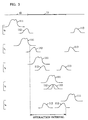
- FIG. 3 depicts the operation of the FIG. 1 arrangement in connection with pulse signals, and demonstrates the advantages derived from the use of material 11 as specified above.
- a segment of fiber 10 with the material of segment 11 included is shown for reference.
- Pulse 111 represents the "pump” signal
- pulse 112 represents the "mark” signal
- pulse 113 represents the "ref” signal; all at time to.
- Pulses 111 and 112 travel through segment 11 from left to right while pulse 113 travels from right to left. Pulse 111 precedes pulse 112, and it is assumed for purposes of FIG. 3, that "pump" pulse 111 travels faster through segment 11 than pulse 112.
- Pulse 113 is shown further to the right from segment 11 than pulse 112 is. This is to demonstrate that segment 11 does not need to be centered within the loop of fiber 10 vis-a-vis coupler 20.
- pulse 112 is shown to be within segment 11 and pulse 111 is just entering segment 11. Pulse 113 is still outside segment 11. At that time, the tail end of pulse 112 and the front end of pulse 111 coincide, and the pulse interaction begins. That is, the propagation speed of the tail end of pulse 112 begins to change in consequence of the front end of pulse 111.
- FIG. 3 depicts pulses 111 and 112 in a more advanced state of interaction, while pulse 113 is within segment 11 but is not interacting with pulse 111.
- pulse 111 is in full interaction with both pulses 112 and 113.
- the tail end of pulse 111 is passing by the front end of pulse 112 and ending the interaction between these two pulses.
- each and every level of pulse 111 interacts with each and every level of pulse 112 over a substantial interval within segment 11; i.e., between times t 1 and t 4 .
- Pulse 111 also interacts with pulse 113 but over a considerably shorter interval; i.e., only in the close neighborhood of time t 3 .
- FIG. 1 arrangement is insensitive to the shape and to the precise timing of the "pump” signal; but it is important to maintain the parameter of the "pump” signal which controls the propagation speed thereof.
- segment 11 is made of birefringent material where the propagation speed of a beam is dependent on the beam's polarization, it is important to maintain polarization.
- the polarization of the "pump” signal is maintained while conserving all of the energy of an applied "pump” signal that has an unknown polarization.
- FIG. 4 an input pulse 21 (of unknown polarization) is applied to a polarization-sensitive splitter 22.
- One output of splitter 22 has TE polarization while the other output has TM polarization.
- the TM polarization output is applied to polarization rotation circuit 23 and the output of circuit 23 (which is TE polarized) is applied to delay circuit 24.
- the TE signal of circuit 22 is combined with the delayed TE signal of circuit 24 in combiner 25 to yield a TE output signal having the shape depicted by pulse 26.
- the delay of circuit 24 is included to insure that the TE signal of circuit 22 does not interfere, constructively or destructively, with the TE signal of circuit 23.
- FIG. 2 circuit can be easily configured to be a multiplexer, a demultiplexer or a NOR gate.
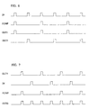
- FIG. 6 depicts the signals arrangement for a demultiplexer application.
- the multiplexed signal is shown at the top, and below it is shown the "pump" signal.
- N being 2 in FIG. 6
- a 1 out of N of the signal line pulses appear at the OUT1 port of the FIG. 2 arrangement.
- the signal pulses not appearing at OUT1 port appear at the OUT2 port of the FIG. 2 arrangement.
- FIG. 7 depicts the signals arrangement for a multiplexer application.
- the two signals to be multiplexed are injected into ports IN and OUT1 of the FIG. 2 arrangement.
- a "pump" pulse appears each time a pulse is injected into port OUT1, the result is that both input signals appear at port OUT2.
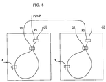
- FIG. 8 The cascadability of our arrangement and the realization of an AND logic gate is depicted in FIG. 8 which includes two switches of the FIG. 2 variety that are cascaded.
- the input marked “P1" " is akin to a power supply input. It injects pulses into the sagnac loop, and results in an output pulses at output Q1 ⁇ when there is no input at the x port.
- a pulse is injected into port x, a corresponding pulse appears at output port Q1.
- That output is injected into port P2 and, if at that time, a pulse is applied at port y, then a pulse appears at output port Q2.
- the AND function results at port Q2 since a pulse signal appears at port Q2 only when both port x and port y supply a signal.
- FIG. 8 depicts an arrangement whereby the FIG. 3 circuit is used to construct an all-optical logic gate
- the circuit can be applied to other uses.
- the FIG. 3 can be applied to regenerate the amplitude and timing of received signals. That is, an optical computing component that is somewhat remote may be sending information to a nearby optical circuit.
- the signal that is expected comprises optical pulses or lack thereof at a particular repetition rate, in synchronism with a clock.
- the objective of the nearby circuit therefore, is to capture the received signal and synchronize it to the local clock.
Landscapes
- Physics & Mathematics (AREA)
- Optics & Photonics (AREA)
- Nonlinear Science (AREA)
- Engineering & Computer Science (AREA)
- General Physics & Mathematics (AREA)
- Electromagnetism (AREA)
- Computer Networks & Wireless Communication (AREA)
- Signal Processing (AREA)
- Plasma & Fusion (AREA)
- Power Engineering (AREA)
- Optical Communication System (AREA)
- Lasers (AREA)
Claims (43)
- Anordnung mit einem Eingangsport zum Empfangen eines optischen Eingangssignals, mit einem Übertragungsmedium mit einem Material (11) mit steuerbarer Ausbreitungsgeschwindigkeit, über welches sich das Eingangssignal ausbreitet, eine Einrichtung (20) zum Injizieren eines Signalpulses, das an den Eingangsport angelegt wird, in das Medium um einen wechselwirkenden Puls (MARK), der sich in dem Medium in eine Richtung ausbreitet, und einen Referenzpuls (REF) zu erzeugen, der sich in dem Medium in die entgegengesetzte Richtung ausbreitet, einer Einrichtung (30) zum steuerbaren Injizieren eines Pumppulses in das Medium, der sich durch das Medium in Richtung des wechselwirkenden Pulses ausbreitet, und mit einer Einrichtung (20) zum Kombinieren des Referenzimpules, nachdem er sich durch das Material ausgebreitet hat, und des wechselwirkenden Puls, nachdem sich dieser durch das Material ausgebreitet hat,
dadurch gekennzeichnet, daß
die Injektionseinrichtung (30) den Pumppuls in Bezug auf den wechselwirkenden Puls zeitlich steuert, damit der Pumppuls den wechselwirkenden Puls durchläuft, während sich der wechselwirkende Puls durch das Material mit steuerbarer Ausbreitungsgeschwindigkeit ausbreitet. - Anordnung nach Anspruch 1, dadurch gekennzeichnet, daß die Einrichtung zum Kombinieren eine interferometrische Kombiniereinrichtung ist.
- Anordnung nch Anspruch 2, dadurch gekennzeichnet, daß die Kombiniereinrichtung dazu dient, ein Ausgangssignal an einem Ausgangsport zu erzeugen, wenn die Pulse, die an der Kombiniereinrichtung anliegen, konstruktiv interferieren.
- Anordnung nach Anspruch 2, dadurch gekennzeichnet, daß die Kombiniereinrichtung dazu dient, ein Ausgangssignal an einem ersten Ausgangsport zu erzeugen, wenn die an die Kombiniereinrichtung angelegten Pulse konstruktiv interferieren, und ein Ausgangssignal an einem zweiten Ausgangsport zu erzeugen, wenn die an die Kombiniereinrichtung angelegten Pulse destruktiv interferieren.
- Anordnung nach einem der Ansprüche 1 bis 4, dadurch gekennzeichnet, daß die Einrichtung zum steuerbaren Injizieren ein oder mehrere Merkmale der folgenden Merkmale umfaßt:
eine Einrichtung zum Injizieren eines Pumppulses etwa dann, wenn sich ein wechselwirkender Puls in dem Übertragungsmedium befindet, eine Einrichtung zum Injizieren eines Pumppulses, wenn kein wechselwirkender Puls im Übertragungsmedium vorhanden ist und eine Einrichtung, dier keinen Puls injiziert, wenn ein wechselwirkender Puls sich im Übertragungsmedium befindet. - Anordnung nach einem der Ansprüche 1 bis 5, dadurch gekennzeichnet, daß das Material mit steuerbarer Ausbreitungsgeschwindigkeit eine Ausbreitungsgeschwindigkeit besitzt, die eine Funktion eines steuerbaren Signalparameters des Pumppulses ist.
- Anordnung nach Anspruch 6, dadurch gekennzeichnet, daß der steuerbare Signalparameter die Wellemlänge des Pumppulses ist.
- Anordnung nach Anspruch 7, ferner gekennzeichnet, durch eine Einrichtung zum Erzeugen des Signalpulses mit einer Wellenlänge und des Pumppulses mit einer anderen Wellenlänge.
- Anordnung nach Anspruch 6, dadurch gekennzeichnet, daß der steuerbare Signalparameter die Polarisation des Pumppulses ist.
- Anordnung nach Anspruch 6, dadurch gekennzeichnet, daß der steuerbare Signalparameter die Intensität des Pumppulses ist.
- Anordnung nach Anspruch 10, dadurch gekennzeichnet, daß der Pumppuls zum Erzeugen einer Intensität gesteuert wird, die eine Phasenverschiebung des wechselwirkenden Pulses erzeugt, der sich durch das Material mit steuerbarer Ausbreitungsgeschwindigkeit zusammen mit dem Pumppuls ausbreitet, die im wesentlichen um π (Bogenmaß) bezüglich der Phasenverschiebung des wechselwirkenden Pulses verändert ist, der ohne den Pumppuls durch das Material mit steuerbarer Ausbreitungsgeschwindigkeit wandert.
- Anordnung nach Anspruch 10, umfassend eine Einrichtung zum Steuern der Intensität des Pumppulses, um eine Phasenverschiebung des Signalimpulses, der durch das Material mit steuerbarer Ausbreitungsgeschwindigkeit in einer Richtung wandert, um im wesentlichen 180° mit Bezug auf die Phasenverschiebung des Signalpulses, der das Material mit steuerbarer Ausbreitungsgeschwindigkeit in der anderen Richtung durchwandert, hervorzurufen.
- Anordnung nach Anspruch 6, dadurch gekennzeichnet, daß der steuerbare Signalparameter die Intensität und die Pclarisation des Pumppulses ist.
- Anordnung nach Anspruch 13, dadurch gekennzeichnet, daß der Pumppuls zum Erzeugen einer Polarisation und einer Intensität gesteuert wird, die eine Phasenverschiebung des wechselwirkenden Pulses erzeugt, der das Material mit steuerbarer Ausbreitungsgeschwindigkeit zusammen mit dem Pumppuls durchwandert, die im wesentlichen um π (Bogenmaß) bezüglich der Phasenverschiebung des wechselwirkenden Pulses verändert ist, der das Material steuerbarer Ausbreitungsgeschwindigkeit ohne den Pumppuls durchwandert.
- Anordnung nach einem der Ansprüche 1 bis 5, dadurch gekennzeichnet, daß das Material mit steuerbarer Ausbreitungsgeschwindigkeit des Übertragungsmediums ein Material ist, in dem sich Signale mit orthogonaler Polarisation mit verschiedenen Geschwindigkeiten ausbreitet und in dem sich die Ausbreitungsgeschwindigkeit für eine gegebene Polarisation, wenn ein Signal mit orthogonaler Polarisation vorhanden ist, von der Ausbreitungsgeschwindigkeit für diese gegebene Polarisation unterscheidet, wenn das Signal mit orthogonaler Polarisation fehlt.
- Anordnung nach Anspruch 15, weiter gekennzeichnet, durch eine Einrichtung zum Erzeugen des wechselwirkenden, polarisierten Pulses und des polarisierten Pumppulses, wobei die Polarisation des wechselwirkenden Pulses zur Polarisation des Pumppulses orthogonal ist.
- Anordnung nach einem der Ansprüche 1 bis 16, dadurch gekennzeichnet, daß die Einrichtung zum Injizieren eines Signalpulses ein Viertor-Koppler ist, dessen erster Port mit dem Eingangsport verbunden ist, dessen zweiter und dritter Port mit den beiden Ports des Übertragungsmediums verbunden sind, wobei die Ports sowohl Eingangs- und als auch Ausgangsports sind und dessen vierter Port einen ersten Ausgangsport der Anordnung bildet.
- Anordnung nach einem der Ansprüche 1 bis 16, dadurch gekennzeichnet, daß der erste Ausgangsport der Anordnung mit der Einrichtung zum Injizieren eines Signalpulses verbunden ist und daß ein Zirkulator (40) zwischen dem Eingangsport der Anordnung und der Einrichtung zur Injizierung eines Signalpulses zwischengeschaltet ist, wobei der Zirkulator einen zweiten Ausgangsport der Anordnung umfaßt.
- Anordnung nach Anspruch 18, gekennzeichnet durch eine Einrichtung zum Steuern des Pumppulses, um ein Ausgangssignal am ersten Ausgangsport der Anordnung zu erzeugen, wenn die Energie des Pumppulses einen ersten Pegel erreicht, und um ein Ausgangssignal am zweiten Ausgangsport der Anordnung zu erzeugen, wenn die Energie des Pumppulses einen zweiten Pegel erreicht.
- Anordnung nach einem der Ansprüche 1 bis 19, gekennzeichnet durch einen Koppler (50), der mit dem Übertragungsmedium zum Extrahieren des im Medium wandernden Pumppulses verbunden ist.
- Anordnung mit einer Verbindung von mehreren Schaltern, dadurch gekennzeichnet, daß jeder Schalter umfaßt:1) einen ersten Eingangsport zum Empfangen eines optischen Eingangssignalpulses,2) einen zweiten Eingangsport zum Empfangen eines Pumppulses,3) einen Ausgangsport,4) ein Übertragungsmedium (10,11) mit einem Material (11) mit steuerbarer Ausbreitungsgeschwindigkeit, durch das sich der Eingangspuls und der Pumppuls ausbreiten kann,5) eine Einrichtung (20) zum Injizieren eines Signalpulses, das am ersten Eingngsport anliegt, in das Medium, um einen wechselwirkenden Puls (MARK) zu erzeugen, der sich im Medium in eine Richtung ausbreitet und zum Erzeugen eines Referenzpulses (REF), der sich im Medium in die entgegengesetzte Richtung ausbreitet, und zum Annehmen von Signalen, die vom Medium eintreffen, um einen Ausgangspuls, der am Ausgangsport anliegt, zu erzeugen, und6) eine Einrichtung (30) zum steuerbaren Injizieren eines Pumppulses, der am zweiten Eingangsport anliegt, in das Medium, wobei sich der Pumppuls durch das Medium in Richtung des wechselwirkenden Pulses ausbreitet und bezüglich dem wechselwirkenden Puls eine Zeitbeziehung besitzt, die bewirkt, daß der Pumppuls den wechselwirkenden Puls durchläuft, während sich der wechselwirkende Puls durch das Material mit steuerbarer Ausbreitungsgeschwindigkeit ausbreitet.
- Anordnung nach Anspruch 21, dadurch gekennzeichnet, daß jeder Schalter einen zweiten Ausgangsport aufweist, der ein Signal von der Einrichtung zum Injizieren eines Signalpulses erhält, wobei das erhaltene Signal zum Signal des ersten Ausgangsports komplementär ist.
- Anordnung nach Anspruch 21, dadurch gekennzeichnet, daß die Schalter einen ersten und einen zweiten Schalter aufweisen, wobei der Ausgangsport des ersten Schalters mit dem ersten Eingangsport des zweiten Schalters verbunden ist.
- Anordnung nach Anspruch 21, dadurch gekenzeichnet, daß die Schalter einen ersten und einen zweiten Schalter aufweisen, wobei der Ausgangsport des ersten Schalters mit dem zweiten Eingangsport des zweiten Schalters verbunden ist.
- Anordnung nach Anspruch 24, dadurch gekennzeichnet, daß der zweite Schalter einen zweiten Ausgangsport aufweist, der ein Signal von der Einrichtung zum Injizieren eines Signalpulses erhält, wobei das erhaltene Signal zum Signal des ersten Ausgangsports komplementär ist.
- Anordnung nach Anspruch 1, dadurch gekennzeichnet, daß die Einrichtung zum Injizieren eines Signalimpules dazu dient, eine Folge von Signalpulsen in den Eingangsport zu injizieren, wobei jeder Signalpuls in der Folge von Signalpulsen einen wechselwirkenden Puls, der sich im Medium in eine Richtung ausbreitet, und einen Referenzpuls erzeugt, der sich im Medium in die entgegengesetzte Richtung ausbreitet, wobei die Einrichtung zum Injizieren eines Pumppulses dazu dient, eine Folge von Pumppulsen in das Medium zu injizieren, die sich im Medium in Richtung des wechselwirkenden Pulses ausbreiten, wobei jeder Pumppuls in der Folge von Pumppulsena) zu einem Zeitpunkt mit Bezug auf einen entsprechenden Signalpuls in der Folge von Signalpulsen injiziert wird, der ermöglicht, daß der entsprechende wechselwirkende Puls durch den Pumppuls hindurchgehen kann, im wesentlichen während sich der Pumppuls und der entsprechende wechselwirkende Puls sich im Material mit steuerbarer Ausbreitungsgeschwindigkeit befinden, undb) in der Intensität zu Zeitpunkten derart gesteuert wird, daß ein Pumppuls hoher Amplitude und ein Pumppuls niedriger Amplitude erzeugt wird.
- Anordnung nach Anspruch 26, dadurch gekennzeichnet, daß die niedrige Amplitude Null oder im wesentlichen Null ist.
- Anordnung nach Anspruch 27, dadurch gekennzeichnet, daß sich abwechselnde Pumppulse in der Folge von Pumppulsen niedrige Amplitude haben.
- Anordnung nach Anspruch 1, dadurch gekennzeichnet, daß die Einrichtung zum Injizieren durch folgende Merkmale gekennzeichnet ist:1) Injizieren in das Übertragungsmedium unter Ansprechen auf einen an einen ersten Signalport angelegten Signalpuls einen Mark-1-Puls, der sich durch das Medium in eine erste Richtung ausbreitet, und einen Referenz-1-Puls, der sich durch das Medium in eine zweite Richtung, die zur ersten Richtung entgegengesetzt ist, ausbreitet, und2) Injizieren in das Übertragungsmedium unter Ansprechen auf einen an einen zweiten Signalport angelegten Signalpuls einen Mark-2-Puls, der sich in eine erste Richtung durch das Medium ausbreitet, und einen Referenz-1-Puls, der sich durch das Medium in eine zweite Richtung ausbreitet,wobei die Einrichtung zum Kombinieren dazu dient, Signale zu kombinieren, die vom Übertragungsmedium eintreffen, um ein erstes Ausgangssignal, das am ersten Signalport angelegt ist, und ein zweites Ausgangssignal, das am zweiten Ausgangsport angelegt ist, zu erzeugen, undwobei das Pumppulssignal einen oder mehrere Pulse umfaßt, wobei ein Puls steuerbar vorhanden ist, wenn sich ein Mark-1-Puls durch das Medium ausbreitet, und steuerbar vorhanden ist, wenn sich ein Mark-2-Puls durch das Medium ausbreitet, und wobei jeder Pumppuls, wenn er vorhanden ist, eine Zeitbeziehung mit Bezug auf den Mark-1- und Mark-2-Puls besitzt, die derart gesteuert wird, daß der Pumppuls den Mark-1- und Mark-2-Puls durchwandert, während der Mark-1- und Mark-2-Puls im wesentlichen innerhalb des Materials mit steuerbarer Ausbreitungsgeschwindigkeit sind.
- Anordnung nach Anspruch 19, ferner gekennzeichnet durch eine Einrichtung zum Anlegen eines Eingangssignals an den ersten Signalport in Form einer Pulsfolge mit einer gegeben Wiederholungsrate und zum Anlegen an einen Pumpsignalport eine Pulsfolge, die die halbe vorgegebene Wiederholungsrate hat, wobei die Folge von Pumpsignalpulsen derart eingestellt ist, daß sie etwa mit jedem anderen der Pulse in der Pulsfolge am ersten Signalport zusammenfällt.
- Anordnung nach Anspruch 29, weiter gekennzeichnet durch eine Einrichtung zum Anlegen eines Eingangssignals an den ersten Signalport in Form einer Pulsfolge mit einer gegebenen Wiederholungsrate und zum Anlegen an einen Pumpsignalport eine Pulsfolge, die die gegebene Wiederholungsrate besitzt, wobei die Folge von Pumpsignalpulsen derart eingestellt ist, daß sie etwa mit den Pulsen in der Folge von Pulsen am ersten Signalport zusammenfällt, wobei das am zweiten Signalport angelegte Eingangssignal eine Pulsfolge ist, die derart eingestellt ist, daß sie nicht mit den Pulsen der Pulsfolge am Pumpsignalport zusammenfällt.
- Anordnung nach Anspruch 1, dadurch gekennzeichnet, daß das Übertragungsmedium eine Sagnac-Interferometerschleife mit wenigstens einem Abschnitt eines Materials mit steuerbarer Ausbreitungsgeschwindigkeit ist.
- Anordnung nach Anspruch 32, dadurch gekennzeichnet, daß die Einrichtung zum steuerbaren Injizieren einer Einrichtung zum Steuern der Intensität des Pumppulses aufweist, um eine konstruktive und destruktive Interferenz des Signalpulses im Koppler des Sagnac-Interferometers zu erzeugen.
- Anrodnung nach Anspruch 32 oder 33, dadurch gekennzeichnet, daß die Einrichtung zu Injizieren eines Pumppulses in der Schleife angeordnet ist.
- Anordnung nach Anspruch 32, dadurch gekennzeichnet, daß die Schleife einen Wellenleiter aufweist.
- Anordnung nach Anspruch 32, dadurch gekennzeichnet, daß die Schleife eine doppelbrechende Faser umfaßt.
- Anordnung nch Anspruch 1, dadurch gekennzeichnet, daß das Übertragungsmedium mehrere Segmente M eines Materials mit steuerbarer Ausbreitungsgeschwindigkeit umfaßt, in denen sich der Signalpuls ausbreitet, wobei der Pumppuls, wenn er injiziert wird, zu einem Zeitpunkt mit Bezug auf den wechselwirkenden Puls injiziert wird, um zu bewirken, daß jeder Punkt des wechselwirkenden Pulses mit jedem Punkt des Pumppulses wechselwirkt, solange sie sich in jedem der Segmente M befinden.
- Anordnung nach Anspruch 37, gekennzeichnet durch einen Rücksetzabschnitt, der zwischen benachbarte Segmente M angeordnet ist und die Position des Pumppulses mit Bezug auf den Wechselwirkungspuls am Eingang des Rücksetzabschnittes zu der Position des Pumppulses mit Bezug auf den Wechselwirkungspuls am Anfang des Segments M, das dem Rücksetzabschnitt vorausgeht, verändert.
- Anordnung nach Anspruch 37, gekennzeichnet durch einen Rücksetzabschnitt, der zwischen benachbarten Segmenten M angeordnet ist und das Zeitverhalten des Pumppulses mit Bezug auf den Wechselwirkungspuls am Eingang des Rücksetzabschnittes zu dem Zeitverhalten des Pumppulses mit Bezug auf den Wechselwirkungspuls am Anfang des Segments M, das dem Rücksetzabschnitt vorausgeht, verändert.
- Anordnung nach Anspruch 38 oder 39, dadurch gekennzeichnet, daß die Rücksetzabschnitte ein Material mit steuerbarer Ausbreitungsgeschwindigkeit umfassen.
- Anordnung nach Anspruch 40, dadurch gekennzeichnet, daß die Segmenete M doppelbrechende Faserabschnitte aufweisen.
- Anordnung nach Anspruch 40 oder 41, dadurch gekennzeichnet, daß die Rücksetzabschnitte doppelbrechende Faserabschnitte aufweisen.
- Anordnung nach Anspruch 42, dadurch gekennzeichnet, daß die Polarisationsorientierung der doppelbrechenden Faserabschnitte der Rücksetzabschnitte zur Polarisationsorientierung der Segmente M orthogonal ist.
Applications Claiming Priority (2)
| Application Number | Priority Date | Filing Date | Title |
|---|---|---|---|
| US521774 | 1990-05-10 | ||
| US07/521,774 US5144375A (en) | 1990-05-10 | 1990-05-10 | Sagnac optical logic gate |
Publications (3)
| Publication Number | Publication Date |
|---|---|
| EP0456422A2 EP0456422A2 (de) | 1991-11-13 |
| EP0456422A3 EP0456422A3 (en) | 1993-04-14 |
| EP0456422B1 true EP0456422B1 (de) | 1997-07-23 |
Family
ID=24078094
Family Applications (1)
| Application Number | Title | Priority Date | Filing Date |
|---|---|---|---|
| EP91304011A Expired - Lifetime EP0456422B1 (de) | 1990-05-10 | 1991-05-03 | Optisches Logikgatter von Sagnac-Typ |
Country Status (4)
| Country | Link |
|---|---|
| US (1) | US5144375A (de) |
| EP (1) | EP0456422B1 (de) |
| JP (1) | JP2628804B2 (de) |
| DE (1) | DE69126913T2 (de) |
Families Citing this family (41)
| Publication number | Priority date | Publication date | Assignee | Title |
|---|---|---|---|---|
| WO1993003406A1 (en) * | 1991-08-09 | 1993-02-18 | Australian And Overseas Telecommunications Corporation Limited | Sagnac loop gates |
| EP0541300A3 (en) * | 1991-11-05 | 1993-09-08 | American Telephone And Telegraph Company | Optical crossbar exchange arrangement |
| US5208705A (en) * | 1991-11-05 | 1993-05-04 | At&T Bell Laboratories | Optical linear feedback shift register |
| US5369520A (en) * | 1992-05-22 | 1994-11-29 | At&T Corp. | Optical regeneration circuit |
| US5673140A (en) * | 1992-09-08 | 1997-09-30 | British Telecommunications Public Limited Company | Non-linear semiconductor optical device |
| US5309267A (en) * | 1992-09-25 | 1994-05-03 | At&T Bell Laboratories | Optical communication system using a Sagnac switch |
| US5295010A (en) * | 1992-10-02 | 1994-03-15 | The Regents Of The University Of Colorado | Amplifying and synchronizing signals in optical computing system |
| US5408351A (en) * | 1992-10-15 | 1995-04-18 | At&T Corp. | Optical communication system |
| US5329393A (en) * | 1992-10-15 | 1994-07-12 | At&T Bell Laboratories | Optical Nyquist rate multiplexer and demultiplexer |
| DE4238103A1 (de) * | 1992-11-12 | 1994-05-19 | Sel Alcatel Ag | Optischer Schalter |
| DE69423548T2 (de) * | 1993-07-21 | 2000-09-14 | At & T Corp., New York | Verbesserter Faserschleifenreflektor zum Zeitdemultiplexen |
| EP0637182A3 (de) * | 1993-07-30 | 1995-11-29 | At & T Corp | Selbstleitweglenkender optischer Kommunikationsknoten und Verwendung von Sagnac Gattern. |
| US5386729A (en) * | 1993-09-22 | 1995-02-07 | The Babcock & Wilcox Company | Temperature compensated microbend fiber optic differential pressure transducer |
| JPH07168217A (ja) * | 1993-12-16 | 1995-07-04 | Nec Corp | 光/光 2×2 スイッチ |
| US5493433A (en) * | 1994-03-02 | 1996-02-20 | Trustees Of Princeton University | Terahertz optical asymmetric demultiplexer |
| US5604618A (en) * | 1994-10-12 | 1997-02-18 | Nippon Telegraph And Telephone Corporation | Optical parametric circuit and optical circuit using the same |
| WO1996028868A2 (en) * | 1995-03-15 | 1996-09-19 | Philips Electronics N.V. | Unit for modulating an optical pulse series in conformity with a data signal |
| WO1996028758A1 (en) * | 1995-03-15 | 1996-09-19 | Philips Electronics N.V. | Optical switch |
| FR2738927B1 (fr) * | 1995-09-14 | 1997-10-17 | Alcatel Nv | Doubleur tout optique |
| US5655039A (en) * | 1995-12-22 | 1997-08-05 | Corning, Inc. | Nonlinear optical loop mirror device including dispersion decreasing fiber |
| US5822471A (en) * | 1997-06-27 | 1998-10-13 | Elsicon, Inc. | Differential optical modulator |
| US5999292A (en) * | 1998-02-20 | 1999-12-07 | The United States Of America As Represented By The Secretary Of The Navy | Sagnac interferometer amplitude modulator based demultiplexer |
| US6393167B1 (en) * | 1998-07-31 | 2002-05-21 | Monica K. Davis | Fast, environmentally-stable fiber switches using a Sagnac interferometer |
| US6389195B1 (en) * | 1999-09-08 | 2002-05-14 | Trw Inc. | Dynamic fiber loop-mirror filter based on pump-induced saturable gain or saturable absorber gratings |
| US6674559B2 (en) | 2001-02-09 | 2004-01-06 | Nortel Networks Limited | Optical automatic gain control based on stable, non-absorbing optical hard limiters |
| US6693732B2 (en) | 2001-02-09 | 2004-02-17 | Nortel Networks Limited | Optical sampler based on stable, non-absorbing optical hard limiters |
| US20020154350A1 (en) * | 2001-02-09 | 2002-10-24 | Johnson Erik V. | Optical logic devices based on stable, non-absorbing optical hard limiters |
| US6516106B2 (en) | 2001-02-09 | 2003-02-04 | Nortel Networks Limited | Subtracting analog noise from an optical communication channel using stable, non-absorbing optical hard limiters |
| US6636337B2 (en) | 2001-02-09 | 2003-10-21 | Nortel Networks Limited | Optical switching device based on stable, non-absorbing optical hard limiters |
| EP1362259A2 (de) * | 2001-02-09 | 2003-11-19 | Nortel Networks Limited | Optische vorrichtung mit einer nichtmonotonen übertragungsfunktion und anwendungen derselben |
| US6671426B2 (en) * | 2001-03-19 | 2003-12-30 | General Instrument Corporation | Monolithic integrated terahertz optical asymmetric demultiplexer |
| US6819819B2 (en) * | 2002-01-08 | 2004-11-16 | Ping Zhou | Method and apparatus for optical communication |
| US7606450B2 (en) * | 2004-08-30 | 2009-10-20 | Poovey Gary N | Light activated optical switch that includes a piezoelectric element and a conductive layer |
| US7532786B2 (en) | 2004-08-30 | 2009-05-12 | Poovey Gary N | Light activated optical switch that includes a piezoelectric element with layers of piezoelectric material having different piezoelectric characteristics |
| US20070206897A1 (en) * | 2006-03-03 | 2007-09-06 | Dr. Shaowen Song | N-nary optical semiconductor transistor and an optical AND gate |
| US7231109B1 (en) | 2006-05-28 | 2007-06-12 | Alan Huang | Ultrafast optical communications system with multiplexer and demultiplexer |
| US20100104242A1 (en) * | 2007-04-12 | 2010-04-29 | Poovey Gary N | Light activated optical switch that includes a piezoelectric element and a conductive layer |
| JP5721427B2 (ja) * | 2007-04-12 | 2015-05-20 | ガルトロニクス・オプティカル・リミテッド | 光スイッチ及び光スイッチを使用した論理ゲート |
| US7644227B1 (en) | 2007-05-31 | 2010-01-05 | Alan Huang | Circulating first-in-first-out buffer |
| EP2247980B1 (de) | 2008-02-29 | 2014-04-16 | Telefonaktiebolaget L M Ericsson (publ) | Optische signalverarbeitung |
| CN102340093A (zh) * | 2010-07-27 | 2012-02-01 | 清华大学 | 光纤锁模激光器 |
Citations (2)
| Publication number | Priority date | Publication date | Assignee | Title |
|---|---|---|---|---|
| FR2253296A1 (en) * | 1973-11-29 | 1975-06-27 | Comp Generale Electricite | Laser pulse generating device - produces pulses of duration 60-400 picoseconds having a determined form |
| EP0183502A2 (de) * | 1984-11-24 | 1986-06-04 | Roke Manor Research Limited | Optische Pulserzeugungssysteme |
Family Cites Families (6)
| Publication number | Priority date | Publication date | Assignee | Title |
|---|---|---|---|---|
| GB2191357B (en) * | 1986-06-07 | 1990-04-25 | Stc Plc | Optical switching |
| CA1298112C (en) * | 1986-10-20 | 1992-03-31 | Nicholas John Doran | Optical device |
| JPS63271313A (ja) * | 1987-04-30 | 1988-11-09 | Nikon Corp | 偏光器 |
| GB8728854D0 (en) * | 1987-12-10 | 1988-01-27 | British Telecomm | Optical device |
| US4995690A (en) * | 1989-04-24 | 1991-02-26 | Islam Mohammed N | Modulation instability-based fiber interferometric switch |
| GB9006675D0 (en) * | 1990-03-26 | 1990-05-23 | British Telecomm | Optical apparatus |
-
1990
- 1990-05-10 US US07/521,774 patent/US5144375A/en not_active Expired - Lifetime
-
1991
- 1991-05-03 EP EP91304011A patent/EP0456422B1/de not_active Expired - Lifetime
- 1991-05-03 DE DE69126913T patent/DE69126913T2/de not_active Expired - Fee Related
- 1991-05-09 JP JP3132184A patent/JP2628804B2/ja not_active Expired - Fee Related
Patent Citations (2)
| Publication number | Priority date | Publication date | Assignee | Title |
|---|---|---|---|---|
| FR2253296A1 (en) * | 1973-11-29 | 1975-06-27 | Comp Generale Electricite | Laser pulse generating device - produces pulses of duration 60-400 picoseconds having a determined form |
| EP0183502A2 (de) * | 1984-11-24 | 1986-06-04 | Roke Manor Research Limited | Optische Pulserzeugungssysteme |
Also Published As
| Publication number | Publication date |
|---|---|
| DE69126913T2 (de) | 1998-02-12 |
| US5144375A (en) | 1992-09-01 |
| JP2628804B2 (ja) | 1997-07-09 |
| JPH04229836A (ja) | 1992-08-19 |
| DE69126913D1 (de) | 1997-08-28 |
| EP0456422A2 (de) | 1991-11-13 |
| EP0456422A3 (en) | 1993-04-14 |
Similar Documents
| Publication | Publication Date | Title |
|---|---|---|
| EP0456422B1 (de) | Optisches Logikgatter von Sagnac-Typ | |
| US5078464A (en) | Optical logic device | |
| Kang et al. | Comparison of Sagnac and Mach–Zehnder ultrafast all-optical interferometric switches based on a semiconductor resonant optical nonlinearity | |
| Jinno et al. | Nonlinear Sagnac interferometer switch and its applications | |
| US5020050A (en) | Cascadable optical combinatorial logic gates | |
| Toliver et al. | Comparison of three nonlinear interferometric optical switch geometries | |
| US5301008A (en) | Optical crossbar exchange arrangement | |
| US5825519A (en) | Optical mach-zehnder time division demultiplexer | |
| EP0541303B1 (de) | Optisches Kreislauf-Schieberegister | |
| US6634813B2 (en) | All-optical bit phase sensing | |
| Kang et al. | Demonstration of ultrafast, all‐optical, low control energy, single wavelength, polarization independent, cascadable, and integratable switch | |
| Bharti et al. | Design and performance analysis of all-optical D and T flip-flop in a polarization rotation based micro-ring resonator | |
| US5206922A (en) | Nonlinear optical switch utilising organic conjugated material and four wave mixing techniques | |
| KR0133473B1 (ko) | 비선형 광섬유 루프거울형 완전 광 스위치 장치 | |
| Wang et al. | All-optical flip-flop based on coupled SOA-PSW | |
| Reis et al. | All‐optical clocked D flip‐flop memory using a hybrid integrated S‐R latch | |
| Wang et al. | All-optical flip-flop based on SOA and MZI switch | |
| Reis et al. | Performance comparison of all-optical clocked SR and D type flip-flops | |
| Stegeman | All-optical switching | |
| Crosignani et al. | Photorefractive solitons | |
| Kang et al. | Ultrafast optical time demultiplexers using semiconductor optical amplifiers | |
| Pasyar et al. | Design of all-optical memory cell using EIT and lasing without inversion phenomena in optical micro ring resonators | |
| Ng et al. | Sagnac-loop phase shifter with polarization-independent operation | |
| Silberberg et al. | All-optical guided-wave devices for switching and routing | |
| Krautschik et al. | Demonstration of demultiplexing with a rocking filter fiber |
Legal Events
| Date | Code | Title | Description |
|---|---|---|---|
| PUAI | Public reference made under article 153(3) epc to a published international application that has entered the european phase |
Free format text: ORIGINAL CODE: 0009012 |
|
| AK | Designated contracting states |
Kind code of ref document: A2 Designated state(s): DE FR GB |
|
| PUAL | Search report despatched |
Free format text: ORIGINAL CODE: 0009013 |
|
| AK | Designated contracting states |
Kind code of ref document: A3 Designated state(s): DE FR GB |
|
| 17P | Request for examination filed |
Effective date: 19931001 |
|
| RAP3 | Party data changed (applicant data changed or rights of an application transferred) |
Owner name: AT&T CORP. |
|
| 17Q | First examination report despatched |
Effective date: 19950328 |
|
| GRAG | Despatch of communication of intention to grant |
Free format text: ORIGINAL CODE: EPIDOS AGRA |
|
| GRAH | Despatch of communication of intention to grant a patent |
Free format text: ORIGINAL CODE: EPIDOS IGRA |
|
| GRAH | Despatch of communication of intention to grant a patent |
Free format text: ORIGINAL CODE: EPIDOS IGRA |
|
| GRAA | (expected) grant |
Free format text: ORIGINAL CODE: 0009210 |
|
| AK | Designated contracting states |
Kind code of ref document: B1 Designated state(s): DE FR GB |
|
| REF | Corresponds to: |
Ref document number: 69126913 Country of ref document: DE Date of ref document: 19970828 |
|
| ET | Fr: translation filed | ||
| PLBE | No opposition filed within time limit |
Free format text: ORIGINAL CODE: 0009261 |
|
| STAA | Information on the status of an ep patent application or granted ep patent |
Free format text: STATUS: NO OPPOSITION FILED WITHIN TIME LIMIT |
|
| 26N | No opposition filed | ||
| PGFP | Annual fee paid to national office [announced via postgrant information from national office to epo] |
Ref country code: GB Payment date: 20010426 Year of fee payment: 11 |
|
| PGFP | Annual fee paid to national office [announced via postgrant information from national office to epo] |
Ref country code: FR Payment date: 20010502 Year of fee payment: 11 |
|
| PGFP | Annual fee paid to national office [announced via postgrant information from national office to epo] |
Ref country code: DE Payment date: 20010629 Year of fee payment: 11 |
|
| REG | Reference to a national code |
Ref country code: GB Ref legal event code: IF02 |
|
| PG25 | Lapsed in a contracting state [announced via postgrant information from national office to epo] |
Ref country code: GB Free format text: LAPSE BECAUSE OF NON-PAYMENT OF DUE FEES Effective date: 20020503 |
|
| PG25 | Lapsed in a contracting state [announced via postgrant information from national office to epo] |
Ref country code: DE Free format text: LAPSE BECAUSE OF NON-PAYMENT OF DUE FEES Effective date: 20021203 |
|
| GBPC | Gb: european patent ceased through non-payment of renewal fee |
Effective date: 20020503 |
|
| PG25 | Lapsed in a contracting state [announced via postgrant information from national office to epo] |
Ref country code: FR Free format text: LAPSE BECAUSE OF NON-PAYMENT OF DUE FEES Effective date: 20030131 |
|
| REG | Reference to a national code |
Ref country code: FR Ref legal event code: ST |