EP0456680B1 - Gruppenantennen - Google Patents
Gruppenantennen Download PDFInfo
- Publication number
- EP0456680B1 EP0456680B1 EP90902313A EP90902313A EP0456680B1 EP 0456680 B1 EP0456680 B1 EP 0456680B1 EP 90902313 A EP90902313 A EP 90902313A EP 90902313 A EP90902313 A EP 90902313A EP 0456680 B1 EP0456680 B1 EP 0456680B1
- Authority
- EP
- European Patent Office
- Prior art keywords
- antenna array
- array
- elements
- feed line
- feed
- Prior art date
- Legal status (The legal status is an assumption and is not a legal conclusion. Google has not performed a legal analysis and makes no representation as to the accuracy of the status listed.)
- Expired - Lifetime
Links
- 238000003491 array Methods 0.000 title claims abstract description 23
- 239000000758 substrate Substances 0.000 claims abstract description 10
- 230000005284 excitation Effects 0.000 claims description 8
- 239000004020 conductor Substances 0.000 claims description 5
- 239000003989 dielectric material Substances 0.000 claims description 3
- 230000000717 retained effect Effects 0.000 claims 1
- 230000005855 radiation Effects 0.000 description 10
- 230000008878 coupling Effects 0.000 description 7
- 238000010168 coupling process Methods 0.000 description 7
- 238000005859 coupling reaction Methods 0.000 description 7
- 238000010276 construction Methods 0.000 description 5
- 238000000926 separation method Methods 0.000 description 5
- RYGMFSIKBFXOCR-UHFFFAOYSA-N Copper Chemical compound [Cu] RYGMFSIKBFXOCR-UHFFFAOYSA-N 0.000 description 2
- 229910052802 copper Inorganic materials 0.000 description 2
- 239000010949 copper Substances 0.000 description 2
- 238000010304 firing Methods 0.000 description 2
- 238000002955 isolation Methods 0.000 description 2
- 239000000463 material Substances 0.000 description 2
- 238000000034 method Methods 0.000 description 2
- 206010033546 Pallor Diseases 0.000 description 1
- 230000005540 biological transmission Effects 0.000 description 1
- 230000001419 dependent effect Effects 0.000 description 1
- RUZYUOTYCVRMRZ-UHFFFAOYSA-N doxazosin Chemical compound C1OC2=CC=CC=C2OC1C(=O)N(CC1)CCN1C1=NC(N)=C(C=C(C(OC)=C2)OC)C2=N1 RUZYUOTYCVRMRZ-UHFFFAOYSA-N 0.000 description 1
- 230000000694 effects Effects 0.000 description 1
- 239000011159 matrix material Substances 0.000 description 1
- 239000002184 metal Substances 0.000 description 1
- 229910052751 metal Inorganic materials 0.000 description 1
- 230000000737 periodic effect Effects 0.000 description 1
- 230000010363 phase shift Effects 0.000 description 1
- 239000004810 polytetrafluoroethylene Substances 0.000 description 1
- 229920001343 polytetrafluoroethylene Polymers 0.000 description 1
- 230000001902 propagating effect Effects 0.000 description 1
- 125000006850 spacer group Chemical group 0.000 description 1
Images





Classifications
-
- H—ELECTRICITY
- H01—ELECTRIC ELEMENTS
- H01Q—ANTENNAS, i.e. RADIO AERIALS
- H01Q21/00—Antenna arrays or systems
- H01Q21/06—Arrays of individually energised antenna units similarly polarised and spaced apart
- H01Q21/061—Two dimensional planar arrays
-
- H—ELECTRICITY
- H01—ELECTRIC ELEMENTS
- H01Q—ANTENNAS, i.e. RADIO AERIALS
- H01Q21/00—Antenna arrays or systems
- H01Q21/0006—Particular feeding systems
- H01Q21/0075—Stripline fed arrays
-
- H—ELECTRICITY
- H01—ELECTRIC ELEMENTS
- H01Q—ANTENNAS, i.e. RADIO AERIALS
- H01Q25/00—Antennas or antenna systems providing at least two radiating patterns
Definitions
- This invention relates to microstrip patch antenna arrays having applications in the fields of communications and radar.
- Microstrip patch antennas are particularly useful for spacecraft and aircraft applications on account of their light weight and flat profile.
- FIG. 1 A section of a conventional microstripline is shown in Fig 1. It comprises a conducting ground plane 1, a dielectric spacer 2 and a conductor 3. For a straight, infinitely long strip, virtually no radiation will occur as long as the separation between the conductor 3 and ground plane 1 is small compared with the wavelength of the propagating wave. However, in the presence of a discontinuity, the field in the gap between the conductor 3 and the ground plane 1 becomes unbalanced and the gap radiates.
- Any patch of microstrip such as the patch 4 shown in Fig 2 has a radiating aperture around its rim. If fields and currents are excited by a stripline feed 5, for example, the patch 4 will radiate.
- the shape of the patch and method and location of its feed determine the field distribution and therefore its radiation characteristics.
- the most commonly used patches are rectangular, square or circular, such patches producing a fairly broad, single beam of radiation in a direction normal to their surfaces and in the case of rectangular patches, producing a controllable polarisation effect.
- Microstrip patches are most commonly used in planar arrays for applications where a narrow beam pattern is required.
- a plan-view of a typical planar microstrip patch array layout is shown in Fig 3. It comprises a plurality of rectangular conducting patches 6 fed via a microstrip feedline 7 which is printed onto the same substrate as the patches.
- the array shown in Fig 3 has a narrow single beam pattern.
- multiple beam arrays have been formed by feeding appropriately grouped radiating elements (microstrip patches, for example) via a "beamforming" circuit.
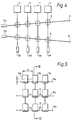
- a well-known example of a beamforming circuit is the so-called Blass matrix which is shown schematically in Fig 4. It comprises a grid of transmission lines and directional couplers 8 which couple input power applied to beam ports 9 and 10 to radiating patches 11 (12a to 12f are matched loads). Patch spacing and interconnecting line lengths determine beam direction. In the arrangement of Fig 4, the number of beams is equal to the number of beam ports.
- the beamforming circuitry is located in close proximity to the patch array, it is a separate entity and can occupy a significant volume. For large arrays with many beams, such matrices are bulky. This is a disadvantage when the antenna is required to be operated in a restricted space.
- the present invention provides a much more compact arrangement in which the antenna and beam forming functions are integrated into a single structure.
- This invention consists of a multiple beam microstrip patch antenna array including N substantially parallel columns and n substantially parallel rows of radiating elements (13) and n feed lines (15), each feed line being coupled to a corresponding one of the n rows of elements in which the n elements within each of the N columns are electrically connected to form linear arrays which are terminated so that a voltage standing wave is produced along the arrays when an appropriate excitation signal is applied to at least one of the feed lines, characterised in that the effective lengths of feed line between adjacent elements along one feed line differ from the effective lengths of feed line between adjacent elements along at least one other feed line.
- the array can be fabricated using microcircuit techniques.
- the coupling between the feed lines and their associated elements is electromagnetic, the elements overlaying the feed line network and being separated therefrom by a dielectric layer.
- the feed line network and elements are formed on the same substrate and the feed lines are directly connected to the appropriate elements.
- a microstrip patch antenna array comprises a network of microstrip patches 13 separated by a dielectric material 14 from a network of feed lines 15 which is in turn separated by the dielectric material 14 from a ground plane 16.
- the microstrip patch network comprises three linear series-connected patch arrays 13a, 13b and 13c, there being three patches in each linear array.
- the network of feed lines which runs underneath the patch network is represented by the dotted lines 15a, 15b and 15c.
- the feed lines are offset from the centre of each patch by a distance 'S' and the lengths of each feed line are different owing to the presence of meanders 17 incorporated in 15b and 15c.
- Each linear patch array is separated from its nearest neighbour by a distance d and each array has an open circuit at each of its ends.
- an RF excitation signal is applied to each of the feed lines 15a, 15b and 15c.
- the separation between adjacent patches in each linear array is chosen so that the array behaves as a resonant element for a particular excitation frequency.
- a voltage standing wave pattern is set up along each linear array as shown in Fig 7.
- the standing wave is periodic along the linear array, it is possible to excite it at any of the voltage peaks.
- any feed line running under the patches can excite a standing wave on each of the linear arrays which results in a narrow pencil beam of radiation.
- the beam direction will always be in a plane perpendicular to the line of each linear array.
- Fig 8 illustrates this.
- Isolation between feed lines is controlled by the coupling at the junction between each feed line and each linear array. Inherently good isolation is likely to be produced by the partial cancellation of each of the small signals coupled into neighbouring feed lines due to the different lengths of each line.
- the coupling is controlled by the separation in height of the feed line network and the patch network and by the offsets 'S' of the feed line from the centre of the patch and by the width of the patch. This coupling is determined by the required amplitude distribution across the array and will be lower for longer arrays.
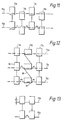
- three feed lines are excited from both ends giving a total of six beams. Approximately equal spacing between beams occurs in each set of three beams as would be expected.
- Circulary polarised beams can be produced using the embodiment of Fig 12 which is similar in construction to the embodiment of Fig 5 in that feed lines 15a, 15b and 15c are overlaid by linear patch arrays 13a, 13b and 13c, in which the rectangular patches in alternate linear arrays (see 13b in Fig 12) are rotated through 90° and connected to one another within each linear array by diagonal interconnections joining alternate ends of each patch.
- the length of each of the feed lines 15a, 15b between adjacent patches is arranged so that the phase of the excitation signal at one patch differs from the phase at its adjacent patch by 90°. Feeding the excitation signal in from the opposite end of the feed line results in beams with the opposite hand of polarisation.
- the invention can be implemented on a single dielectric layer as shown in the embodiment of Fig 13.
- the feed lines 15a, 15b are directly connected to the patch sides with the dimension 'S controlling the coupling level. This results in simpler construction although unwanted radiation from the feed lines is greater than for the multilayer construction of the embodiments illustrated in Figs 5, 11 and 12.
- Direct coupling of the feed and array lines can be usefully employed in a balanced stripline construction such as that illustrated in Figs 14 and 15.
- This construction comprises three superimposed layers 16, 17 and 18 of etched copper on substrate maintaining a separation d between the conducting layers.
- the middle layer 17 consists of a network in which meandering feedlines 19 interconnect with array lines 20.
- the top and bottom layers 16 and 18 comprise identical arrays of rectangular slots 21 formed in the copper layer which, when assembled, are located symmetrically on either side of the middle layer, over - and under - lying the array lines 20.
- both the feed lines 22 and the transverse resonant arrays 23 are made of waveguide material, coupled together by small holes in the common wall at each intersection.
- the arrays themselves are formed by conventional waveguide slots 24.
- the feed lines are made to have different effective lengths by one of the numerous ways of providing phase shifts in a waveguide, such as an iris, a screw extending in from the waveguide wall, or a section of dielectric.
- a terminating impedance 25 is arranged to interconnect the ground plane 26 and the remote edge of the end patch 39 of each array.
- a patch of lossy material may be placed on the feedline substrate in a position underlying portions of the end patch of each array.
- the feedlines 28 comprise suspended stripline feeds in each of which a conducting stripline element 29 is located on a thin substrate film 30 centrally within a waveguide box 31 (Alternatively all the striplines could be configured on a single substrate within an extended waveguide).
- the antenna arrays comprise series of square or rectangular cavities 32 (see Fig 20) interconnected by coaxial lines 33 and coupled to the feedlines by small holes 34 in the roof of the waveguide. The cavities either radiate directly through small holes or, as shown in the drawing, they can feed short horn elements 35.
- the effective lengths of the stripline elements 29 differ from one another, as before.
Landscapes
- Variable-Direction Aerials And Aerial Arrays (AREA)
- Waveguide Aerials (AREA)
- Radar Systems Or Details Thereof (AREA)
Claims (13)
- Mehrstrahl-Microstrip-Strahler-Gruppenantenne mit N im wesentlichen parallelen Spalten und n im wesentlichen parallelen Zeilen von Strahlerelementen (13) und n Versorgungsleitungen (15) wobei jede Zufuhrleitung jeweils mit einer der n Zeilen von Elementen gekoppelt ist, in welcher die n Elemente innerhalb jeder der N Spalten elektrisch verbunden sind, so daß sie lineare Gruppen bilden, welche abgeschlossen sind, so daß sich eine stehende Spannungswelle entlang der Gruppe ergibt, wenn ein entsprechendes Erregungssignal an wenigstens eine der n Zufuhrleitungen angelegt wird,
dadurch gekennzeichnet, daß
sich die effektiven Längen der Zufuhrleitungen zwischen benachbarten Elementen entlang einer Zufuhrleitung von den effektiven Längen der Zufuhrleitungen zwischen benachbarten Elementen entlang wenigstens einer anderen Zufuhrleitung unterscheiden. - Gruppenantenne nach Anspruch 1, bei welcher die Strahlerelemente (13) die Zufuhrleitungen bedecken und von diesen durch ein dielektrisches Material (14) getrennt sind.
- Gruppenantenne nach einem der vorangehenden Ansprüche, bei welcher jede Spalte Strahlerelemente umfaßt, die als miteinander verbundene metallische rechteckige Flächen auf einem dielektrischen Substrat aufgebracht sind.
- Gruppenantenne nach einem der vorangehenden Ansprüche, bei welcher jede Zufuhrleitung (15) in derselben Richtung von dem Zentrum jeden Elementes (13) aus versetzt ist, mit welchem sie verbunden ist.
- Gruppenantenne nach einem der Ansprüche 1 - 3, bei welcher jede Zufuhrleitung (15) in wechselnden Richtungen von dem Zentrum jeden Elementes (13) aus versetzt ist, mit dem sie verbunden ist.
- Gruppenantenne nach einem der Ansprüche 1 - 3, bei welcher die Elemente (13) rechteckig sind und in aufeinanderfolgenden Spalten alternierend transvers zu (36) bzw. in Reihe mit (37) den Zufuhrleitungen (15) liegen, wobei die in Linie liegenden Elemente (37) miteinander durch diagonale Verbindungen (38) verbunden sind, die wechselseitige Enden von jedem Element miteinander verbinden.
- Gruppenantenne nach einem der vorangehenden Ansprüche, bei welcher jede lineare Gruppe (13) durch eine Impedanz (25) abgeschlossen ist, die zwischen seinen Endelementen (39) und einer Masseplatte (26) liegen.
- Gruppenantenne nach einem der Ansprüche 1, 2, 4 oder 5, bei welcher die Gruppen-Elemente die Form von Schlitzen (21) in einem Blatt von leitfähigem Material haben.
- Gruppenantenne nach Anspruch 1, bei welcher die Versorgungsleitungen die Form von aufgehängten Streifenleitungen (28) haben, wobei ein leitendes Element (29) innerhalb einer Box (31) rechteckiger Form gehalten wird.
- Gruppenantenne nach Anspruch 1, bei welcher die Versorgungsleitungen die Form von Wellenleitern (22) haben, die mit den linearen Gruppen (23) an gleich beabstandeten Orten verbunden sind, wobei die effektiven Längen zwischen den besagten Orten vorgegeben sind durch die Einführung von Phasenverzögerungsvorrichtungen innerhalb des Wellenleiters.
- Gruppenantenne nach einem der Ansprüche 1, 9 oder 10, bei welcher die Gruppen-Elemente miteinander verbundene Cavities (32) umfassen.
- Gruppenantenne nach Anspruch 11, bei welcher jede Cavity einen hornförmigen Strahler (35) hat.
- Gruppenantenne nach einem der vorangehenden Ansprüche, bei welcher die Versorgungsleitungen symmetrisch zwischen zwei identischen Gruppen (16, 18) von Gruppen-Elementen angeordnet sind.
Applications Claiming Priority (3)
| Application Number | Priority Date | Filing Date | Title |
|---|---|---|---|
| GB8902421 | 1989-02-03 | ||
| GB898902421A GB8902421D0 (en) | 1989-02-03 | 1989-02-03 | Antenna array |
| PCT/GB1990/000141 WO1990009042A1 (en) | 1989-02-03 | 1990-01-31 | Antenna arrays |
Publications (2)
| Publication Number | Publication Date |
|---|---|
| EP0456680A1 EP0456680A1 (de) | 1991-11-21 |
| EP0456680B1 true EP0456680B1 (de) | 1994-11-30 |
Family
ID=10651079
Family Applications (1)
| Application Number | Title | Priority Date | Filing Date |
|---|---|---|---|
| EP90902313A Expired - Lifetime EP0456680B1 (de) | 1989-02-03 | 1990-01-31 | Gruppenantennen |
Country Status (6)
| Country | Link |
|---|---|
| US (1) | US5210541A (de) |
| EP (1) | EP0456680B1 (de) |
| JP (1) | JP2977893B2 (de) |
| DE (1) | DE69014607T2 (de) |
| GB (1) | GB8902421D0 (de) |
| WO (1) | WO1990009042A1 (de) |
Families Citing this family (44)
| Publication number | Priority date | Publication date | Assignee | Title |
|---|---|---|---|---|
| US5448252A (en) * | 1994-03-15 | 1995-09-05 | The United States Of America As Represented By The Secretary Of The Air Force | Wide bandwidth microstrip patch antenna |
| EP0763264A1 (de) * | 1994-06-03 | 1997-03-19 | Telefonaktiebolaget Lm Ericsson | Gruppenantenne aus mikrostreifenleitern |
| US6157343A (en) * | 1996-09-09 | 2000-12-05 | Telefonaktiebolaget Lm Ericsson | Antenna array calibration |
| JP3106895B2 (ja) * | 1995-03-01 | 2000-11-06 | 松下電器産業株式会社 | 電磁放射測定装置 |
| JPH08274529A (ja) * | 1995-03-31 | 1996-10-18 | Toshiba Corp | アレイアンテナ装置 |
| SE505476C2 (sv) * | 1996-06-12 | 1997-09-01 | Ericsson Telefon Ab L M | Anordning och förfarande vid signalöverföring |
| JP3761988B2 (ja) * | 1996-09-18 | 2006-03-29 | 本田技研工業株式会社 | アンテナ装置 |
| SE508297C2 (sv) * | 1997-01-03 | 1998-09-21 | Ericsson Telefon Ab L M | Elektronikenhet för trådlös signalöverföring |
| US6011522A (en) * | 1998-03-17 | 2000-01-04 | Northrop Grumman Corporation | Conformal log-periodic antenna assembly |
| US6018323A (en) * | 1998-04-08 | 2000-01-25 | Northrop Grumman Corporation | Bidirectional broadband log-periodic antenna assembly |
| US6081235A (en) * | 1998-04-30 | 2000-06-27 | The United States Of America As Represented By The Administrator Of The National Aeronautics And Space Administration | High resolution scanning reflectarray antenna |
| US6140965A (en) * | 1998-05-06 | 2000-10-31 | Northrop Grumman Corporation | Broad band patch antenna |
| US6181279B1 (en) | 1998-05-08 | 2001-01-30 | Northrop Grumman Corporation | Patch antenna with an electrically small ground plate using peripheral parasitic stubs |
| JP2000040915A (ja) * | 1998-07-23 | 2000-02-08 | Alps Electric Co Ltd | 平面アンテナ |
| US6078223A (en) * | 1998-08-14 | 2000-06-20 | The United States Of America As Represented By The Administrator Of The National Aeronautics And Space Administration | Discriminator stabilized superconductor/ferroelectric thin film local oscillator |
| EP0999728A1 (de) * | 1998-11-04 | 2000-05-10 | TELEFONAKTIEBOLAGET L M ERICSSON (publ) | Elektrisches Bauelement und elektrisches Schaltungsmodul mit verbundenen Erdungsflächen |
| US6292133B1 (en) | 1999-07-26 | 2001-09-18 | Harris Corporation | Array antenna with selectable scan angles |
| FR2807876B1 (fr) * | 2000-04-18 | 2002-06-21 | Ct Regional D Innovation Et De | Antenne plaque micro-onde |
| US6388621B1 (en) * | 2000-06-20 | 2002-05-14 | Harris Corporation | Optically transparent phase array antenna |
| DE10057564A1 (de) * | 2000-11-21 | 2002-05-23 | Volkswagen Ag | Ansteuernetzwerk für eine Antennenanordnung eines Radarsensors, Radarantenne und Radarsensor |
| US7009557B2 (en) | 2001-07-11 | 2006-03-07 | Lockheed Martin Corporation | Interference rejection GPS antenna system |
| AU2003290935C1 (en) * | 2002-11-15 | 2008-11-06 | Lockheed Martin Corporation | All-weather precision guidance and navigation system |
| FI114756B (fi) * | 2003-02-14 | 2004-12-15 | Vaisala Oyj | Menetelmä ja laite kulkuaaltoantennin tehonjaon ohjaamiseksi |
| US7053853B2 (en) * | 2003-06-26 | 2006-05-30 | Skypilot Network, Inc. | Planar antenna for a wireless mesh network |
| US20060071849A1 (en) * | 2004-09-30 | 2006-04-06 | Lockheed Martin Corporation | Tactical all weather precision guidance and navigation system |
| US7576655B2 (en) * | 2005-03-29 | 2009-08-18 | Accu-Sort Systems, Inc. | RFID conveyor system and method |
| US7639191B2 (en) | 2005-07-04 | 2009-12-29 | Telefonaktiebolaget L M Ericsson (Publ) | Multi beam repeater antenna for increased coverage |
| EP1900114A1 (de) * | 2005-07-04 | 2008-03-19 | TELEFONAKTIEBOLAGET LM ERICSSON (publ) | Passiv-repeater-antenne |
| CN101218710B (zh) * | 2005-07-04 | 2012-11-14 | 艾利森电话股份有限公司 | 用于点对点应用的改进转发天线 |
| TWI385858B (zh) * | 2008-09-26 | 2013-02-11 | Advanced Connectek Inc | Array antenna |
| WO2010068954A1 (en) * | 2008-12-12 | 2010-06-17 | Wavebender, Inc. | Integrated waveguide cavity antenna and reflector dish |
| US8854212B2 (en) | 2009-03-30 | 2014-10-07 | Datalogic Automation, Inc. | Radio frequency identification tag identification system |
| US8558745B2 (en) * | 2010-10-13 | 2013-10-15 | Novatrans Group Sa | Terahertz antenna arrangement |
| US8952863B2 (en) * | 2010-12-17 | 2015-02-10 | Nokia Corporation | Strain-tunable antenna and associated methods |
| ES2698126T3 (es) | 2012-12-14 | 2019-01-31 | Bae Systems Plc | Mejoras en antenas |
| GB2508899B (en) * | 2012-12-14 | 2016-11-02 | Bae Systems Plc | Improvements in antennas |
| US9361493B2 (en) | 2013-03-07 | 2016-06-07 | Applied Wireless Identifications Group, Inc. | Chain antenna system |
| US10033082B1 (en) * | 2015-08-05 | 2018-07-24 | Waymo Llc | PCB integrated waveguide terminations and load |
| US10320087B2 (en) * | 2016-01-15 | 2019-06-11 | Huawei Technologies Co., Ltd. | Overlapping linear sub-array for phased array antennas |
| EP3285334A1 (de) * | 2016-08-15 | 2018-02-21 | Nokia Solutions and Networks Oy | Strahlformungsantennengruppe |
| WO2018154309A1 (en) * | 2017-02-23 | 2018-08-30 | Oxford University Innovation Ltd. | Signal coupler |
| JP6756300B2 (ja) * | 2017-04-24 | 2020-09-16 | 株式会社村田製作所 | アレーアンテナ |
| DE102017218823A1 (de) * | 2017-10-20 | 2019-04-25 | Fraunhofer-Gesellschaft zur Förderung der angewandten Forschung e.V. | Antennenanordnung zum Abtasten eines Raumes mittels sichtbarer oder unsichtbarer Strahlung |
| KR102666163B1 (ko) * | 2021-03-04 | 2024-05-14 | (주)스마트레이더시스템 | 타겟 검출용 레이더 장치 |
Family Cites Families (8)
| Publication number | Priority date | Publication date | Assignee | Title |
|---|---|---|---|---|
| US3775771A (en) * | 1972-04-27 | 1973-11-27 | Textron Inc | Flush mounted backfire circularly polarized antenna |
| GB1529541A (en) * | 1977-02-11 | 1978-10-25 | Philips Electronic Associated | Microwave antenna |
| US4347516A (en) * | 1980-07-09 | 1982-08-31 | The Singer Company | Rectangular beam shaping antenna employing microstrip radiators |
| US4450449A (en) * | 1982-02-25 | 1984-05-22 | Honeywell Inc. | Patch array antenna |
| US4780723A (en) * | 1986-02-21 | 1988-10-25 | The Singer Company | Microstrip antenna compressed feed |
| US4937585A (en) * | 1987-09-09 | 1990-06-26 | Phasar Corporation | Microwave circuit module, such as an antenna, and method of making same |
| FR2622055B1 (fr) * | 1987-09-09 | 1990-04-13 | Bretagne Ctre Regl Innova Tran | Antenne plaque microonde, notamment pour radar doppler |
| US4912481A (en) * | 1989-01-03 | 1990-03-27 | Westinghouse Electric Corp. | Compact multi-frequency antenna array |
-
1989
- 1989-02-03 GB GB898902421A patent/GB8902421D0/en active Pending
-
1990
- 1990-01-31 DE DE69014607T patent/DE69014607T2/de not_active Expired - Lifetime
- 1990-01-31 JP JP2502382A patent/JP2977893B2/ja not_active Expired - Lifetime
- 1990-01-31 EP EP90902313A patent/EP0456680B1/de not_active Expired - Lifetime
- 1990-01-31 WO PCT/GB1990/000141 patent/WO1990009042A1/en not_active Ceased
- 1990-01-31 US US07/762,006 patent/US5210541A/en not_active Expired - Lifetime
Also Published As
| Publication number | Publication date |
|---|---|
| US5210541A (en) | 1993-05-11 |
| DE69014607T2 (de) | 1995-04-13 |
| JPH04503133A (ja) | 1992-06-04 |
| WO1990009042A1 (en) | 1990-08-09 |
| GB8902421D0 (en) | 1989-03-22 |
| DE69014607D1 (de) | 1995-01-12 |
| JP2977893B2 (ja) | 1999-11-15 |
| EP0456680A1 (de) | 1991-11-21 |
Similar Documents
| Publication | Publication Date | Title |
|---|---|---|
| US5210541A (en) | Microstrip patch antenna arrays | |
| US4623894A (en) | Interleaved waveguide and dipole dual band array antenna | |
| US4170013A (en) | Stripline patch antenna | |
| US6211824B1 (en) | Microstrip patch antenna | |
| CA1328923C (en) | Plural layer coupling system | |
| US4464663A (en) | Dual polarized, high efficiency microstrip antenna | |
| EP0398555B1 (de) | Leichte und flache phasengesteuerte Gruppenantenne mit elektromagnetisch gekoppelten integrierten Untergruppen | |
| EP0329079B1 (de) | Antenne mit geschlitztem Hohlleiter | |
| US6507320B2 (en) | Cross slot antenna | |
| EP0360861B1 (de) | Zirkular polarisierte streifenleitungsantennengruppe | |
| US7450071B1 (en) | Patch radiator element and array thereof | |
| EP0005642B1 (de) | Streifenleitungsantenne | |
| US3987455A (en) | Microstrip antenna | |
| JPH0671171B2 (ja) | 広帯域アンテナ | |
| GB2323970A (en) | A cavity-backed microstrip dipole antenna array | |
| NO336361B1 (no) | Todimensjonal elektronisk avsøkt gruppeantenne med kompakt CTS-mating og MEMS-faseforskyvere | |
| JPS581846B2 (ja) | 放射スロツト開口のアンテナアレイ | |
| JPH08181537A (ja) | マイクロ波アンテナ | |
| EP3979409B1 (de) | Antennenstrukturen mit hoher verstärkung und strahlenfächer und zugehörige antenne in einem gehäuse | |
| US20070176846A1 (en) | Radiation controller including reactive elements on a dielectric surface | |
| US12062863B2 (en) | Antenna device | |
| US11394114B2 (en) | Dual-polarized substrate-integrated 360° beam steering antenna | |
| US4507664A (en) | Dielectric image waveguide antenna array | |
| EP0542447B1 (de) | Ebene Plattenantenne | |
| JP5657742B2 (ja) | アンテナ |
Legal Events
| Date | Code | Title | Description |
|---|---|---|---|
| PUAI | Public reference made under article 153(3) epc to a published international application that has entered the european phase |
Free format text: ORIGINAL CODE: 0009012 |
|
| 17P | Request for examination filed |
Effective date: 19910726 |
|
| AK | Designated contracting states |
Kind code of ref document: A1 Designated state(s): AT BE CH DE DK ES FR GB IT LI LU NL SE |
|
| 17Q | First examination report despatched |
Effective date: 19931027 |
|
| RBV | Designated contracting states (corrected) |
Designated state(s): DE FR IT NL SE |
|
| RBV | Designated contracting states (corrected) |
Designated state(s): DE FR GB IT NL SE |
|
| GRAA | (expected) grant |
Free format text: ORIGINAL CODE: 0009210 |
|
| ITF | It: translation for a ep patent filed | ||
| AK | Designated contracting states |
Kind code of ref document: B1 Designated state(s): DE FR GB IT NL SE |
|
| ET | Fr: translation filed | ||
| REF | Corresponds to: |
Ref document number: 69014607 Country of ref document: DE Date of ref document: 19950112 |
|
| EAL | Se: european patent in force in sweden |
Ref document number: 90902313.7 |
|
| PLBE | No opposition filed within time limit |
Free format text: ORIGINAL CODE: 0009261 |
|
| STAA | Information on the status of an ep patent application or granted ep patent |
Free format text: STATUS: NO OPPOSITION FILED WITHIN TIME LIMIT |
|
| 26N | No opposition filed | ||
| REG | Reference to a national code |
Ref country code: GB Ref legal event code: 732E |
|
| REG | Reference to a national code |
Ref country code: GB Ref legal event code: IF02 |
|
| REG | Reference to a national code |
Ref country code: FR Ref legal event code: TP |
|
| NLS | Nl: assignments of ep-patents |
Owner name: QINETIQ LIMITED |
|
| PGFP | Annual fee paid to national office [announced via postgrant information from national office to epo] |
Ref country code: NL Payment date: 20021212 Year of fee payment: 14 |
|
| PGFP | Annual fee paid to national office [announced via postgrant information from national office to epo] |
Ref country code: SE Payment date: 20021230 Year of fee payment: 14 |
|
| PG25 | Lapsed in a contracting state [announced via postgrant information from national office to epo] |
Ref country code: SE Free format text: LAPSE BECAUSE OF NON-PAYMENT OF DUE FEES Effective date: 20040201 |
|
| PG25 | Lapsed in a contracting state [announced via postgrant information from national office to epo] |
Ref country code: NL Free format text: LAPSE BECAUSE OF NON-PAYMENT OF DUE FEES Effective date: 20040801 |
|
| EUG | Se: european patent has lapsed | ||
| NLV4 | Nl: lapsed or anulled due to non-payment of the annual fee |
Effective date: 20040801 |
|
| PG25 | Lapsed in a contracting state [announced via postgrant information from national office to epo] |
Ref country code: IT Free format text: LAPSE BECAUSE OF NON-PAYMENT OF DUE FEES;WARNING: LAPSES OF ITALIAN PATENTS WITH EFFECTIVE DATE BEFORE 2007 MAY HAVE OCCURRED AT ANY TIME BEFORE 2007. THE CORRECT EFFECTIVE DATE MAY BE DIFFERENT FROM THE ONE RECORDED. Effective date: 20050131 |
|
| PGFP | Annual fee paid to national office [announced via postgrant information from national office to epo] |
Ref country code: DE Payment date: 20090122 Year of fee payment: 20 |
|
| PGFP | Annual fee paid to national office [announced via postgrant information from national office to epo] |
Ref country code: GB Payment date: 20090122 Year of fee payment: 20 |
|
| PGFP | Annual fee paid to national office [announced via postgrant information from national office to epo] |
Ref country code: FR Payment date: 20090115 Year of fee payment: 20 |
|
| REG | Reference to a national code |
Ref country code: GB Ref legal event code: PE20 Expiry date: 20100130 |
|
| PG25 | Lapsed in a contracting state [announced via postgrant information from national office to epo] |
Ref country code: GB Free format text: LAPSE BECAUSE OF EXPIRATION OF PROTECTION Effective date: 20100130 |
|
| PG25 | Lapsed in a contracting state [announced via postgrant information from national office to epo] |
Ref country code: DE Free format text: LAPSE BECAUSE OF EXPIRATION OF PROTECTION Effective date: 20100131 |