EP0457306A2 - Procédé et dispositif pour lire et écrire une mémoire de données à microprocesseur, en particulier d'un appareil de comptage ou de mesure d'enregistrement - Google Patents
Procédé et dispositif pour lire et écrire une mémoire de données à microprocesseur, en particulier d'un appareil de comptage ou de mesure d'enregistrement Download PDFInfo
- Publication number
- EP0457306A2 EP0457306A2 EP91107872A EP91107872A EP0457306A2 EP 0457306 A2 EP0457306 A2 EP 0457306A2 EP 91107872 A EP91107872 A EP 91107872A EP 91107872 A EP91107872 A EP 91107872A EP 0457306 A2 EP0457306 A2 EP 0457306A2
- Authority
- EP
- European Patent Office
- Prior art keywords
- data
- head
- read
- scanning head
- data memory
- Prior art date
- Legal status (The legal status is an assumption and is not a legal conclusion. Google has not performed a legal analysis and makes no representation as to the accuracy of the status listed.)
- Withdrawn
Links
Images




Classifications
-
- H—ELECTRICITY
- H04—ELECTRIC COMMUNICATION TECHNIQUE
- H04B—TRANSMISSION
- H04B5/00—Near-field transmission systems, e.g. inductive or capacitive transmission systems
- H04B5/70—Near-field transmission systems, e.g. inductive or capacitive transmission systems specially adapted for specific purposes
- H04B5/77—Near-field transmission systems, e.g. inductive or capacitive transmission systems specially adapted for specific purposes for interrogation
-
- G—PHYSICS
- G01—MEASURING; TESTING
- G01R—MEASURING ELECTRIC VARIABLES; MEASURING MAGNETIC VARIABLES
- G01R15/00—Details of measuring arrangements of the types provided for in groups G01R17/00 - G01R29/00, G01R33/00 - G01R33/26 or G01R35/00
- G01R15/14—Adaptations providing voltage or current isolation, e.g. for high-voltage or high-current networks
- G01R15/22—Adaptations providing voltage or current isolation, e.g. for high-voltage or high-current networks using light-emitting devices, e.g. LED, optocouplers
-
- G—PHYSICS
- G06—COMPUTING OR CALCULATING; COUNTING
- G06M—COUNTING MECHANISMS; COUNTING OF OBJECTS NOT OTHERWISE PROVIDED FOR
- G06M3/00—Counters with additional facilities
-
- G—PHYSICS
- G08—SIGNALLING
- G08C—TRANSMISSION SYSTEMS FOR MEASURED VALUES, CONTROL OR SIMILAR SIGNALS
- G08C17/00—Arrangements for transmitting signals characterised by the use of a wireless electrical link
- G08C17/04—Arrangements for transmitting signals characterised by the use of a wireless electrical link using magnetically coupled devices
Definitions
- the invention relates to a method for reading and / or reading data in a microprocessor-controlled data memory, in particular a registering measuring or counting device, in which the data are transmitted between the data memory and a read-in device via an interface with a wireless signal connection.
- a known device for this purpose contains an optical scanning head connected to electronic evaluation and input units with optoelectronic transducers for delivering and receiving optical signals, while the data memory of the meter is equipped with a corresponding optical transmission head with optoelectronic transducers and the interface by spatial proximity of the scanning head and transmitter head is formed to achieve an optical signal path.
- the person reading the meter then only needs to place the optical scanning head of a portable read-in device carried along at a predetermined location on the outer wall of the meter housing, behind which the transmitter head is located, and all data can then be transmitted automatically.
- a problem that arises in this case is that the reading out of data in the manner described above requires a portion of electrical energy on the meter side which is substantially greater than the portion of energy occurring in normal operation.
- the invention has for its object to provide a method of the type specified in the preamble of claim 1, by means of which it is possible, in particular, to read out data in a manner which does not burden the voltage source of the microprocessor-controlled data memory. Furthermore, a device for carrying out this method should be created which is simple in construction and can be handled in a very simple and safe manner.
- a particularly advantageous device for carrying out the method according to the invention in which the data transmission between the data memory and the read-in device takes place via an interface with an optical signal path, is described in claim 4.
- Advantageous embodiments of this device are the subject of claims 5 to 7.
- Further exemplary embodiments of devices for carrying out the method according to the invention are described in claims 8 to 12.
- the basic idea of the invention is not only to read or read data between the data storage device and the read-in and read-out device via an interface with a wireless signal connection, but also to wirelessly transmit the energy required in particular for reading from outside, that is to say from the read-in device. feed. In this way, stress on the voltage source of the data storage device during the readout process is avoided.
- the supply of energy by means of a high-frequency signal by induction has proven to be particularly easy to use and advantageous.
- the method with inductive energy transmission leads to particularly simple and easy-to-use devices.
- This can be done, for example, by means of a frequency-modulated carrier signal.
- an additional data channel is created without influencing the energy transmission, which is independent of the optical transmission path.
- the interface can only be put into operation if the high-frequency carrier signal is present. This provides additional protection against unauthorized data manipulation.
- the method according to the invention is primarily intended for reading heat meters, gas meters and the like, but it can also be used for reading other externally readable data memories and can also be used with meters that are connected to their own electrical power supply.
- the latter has the advantage that reading devices can be created which can be used with very different types of meter provided with standardized reading devices.
- This type of wireless energy supply for reading data has the additional advantage that a so-called "hardware interrupt" is triggered by the approach of the scanning head of the read-in device to the sending head and the associated application of the operating voltage to the reading unit of the data memory in a counter processor can be.
- This processor then ends the measurement and carries out data communication via the wireless interface. A recurring interruption of the measurement in order to check whether information is present at the interface is no longer necessary.
- a complex time synchronization between the reading device and reading counter can also be omitted.
- the use of the method and the devices according to the invention is not limited to reading meters. Rather, the data can also be entered into the data memories of registering measuring or counting devices with external energy supply via the wireless interface, for example when checking the counting devices or in order to perform certain control functions. This enables the battery of the data storage device to be supported even with this electricity-intensive work.
- the method according to the invention and the devices for this purpose are not only limited to use on meters, but can also be used in other microprocessor-controlled data memories in which the transmission of data to an external read-in device takes place via an interface with a wireless signal connection.
- the method according to the invention also has the advantage that the microprocessor-controlled data memory or the entire counter containing this data memory can be spatially relatively far away from the interface for data transmission, because due to the inventive method of supplying energy relatively long line lengths between the interface and the data memory are available can be taken.
- induction coils can be arranged concentrically one inside the other on the scanning head and on the transmitting head. With an arrangement of three induction coils in this way, three mutually independent transmission channels are obtained, one of which can be used for transmitting the energy, another for transmitting data in one direction and the third for transmitting data in the opposite direction. On the other hand, however, it is also possible to obtain a plurality of transmission channels with a number of induction coils that are smaller than the number of transmission channels by appropriate circuitry measures.
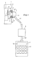
- Fig. 1 is a highly schematic, for example, for district heating metering, shown with a housing 1 and a microprocessor-controlled data memory 2, which has a feed input 2.1, a data output 2.2 and a data input 2.3.
- the inputs-outputs 2.1, 2.2 and 2.3 are connected to a component 3, which is referred to below as the "transmitter head", although data is transmitted in both directions via this component.
- the function of this transmitter head 3 is explained in more detail below.
- a component 4 is releasably attached, which is referred to below as a “scanning head", although data can also be transmitted in both directions through this component.
- the function of this component is also explained in more detail below.
- the scanning head 4 has on its front side a ring magnet 4.3 with which it is achieved that the scanning head 4 attached to the housing wall 1.1 made of ferromagnetic material adheres there.
- the scanning head 4 is connected via a line 5.1 to a device 6 which contains a transmitter and amplifier in a manner described in more detail below. It is also connected via a line 5.2 to a device 7 which contains input and evaluation units and is provided on its top with a keyboard 7.1 and a display field of view 7.2.
- the devices 4, 6 and 7 together form a read-in device for the data memory 2 of the meter.
- the more precise design of the evaluation and input units contained in the device 7 is not shown in the following, because these are circuits which are known per se.
- the transmission of data between the data memory 2 and the read-in device 4-6-7 takes place in the direction from the data memory 2 via the transmission head 3, which for this purpose has a middle part 3.2, which contains optoelectronic converters, and which has a middle part 4.2 on the scanning head 4, which likewise contains optoelectronic converters, so that a wireless optical signal path for transmitting data in both directions is formed through an opening 1.2 in the housing wall 1.1.
- an induction coil 4.1 surrounding the front part thereof is arranged on the scanning head 4, which is opposite an induction coil 3.1 surrounding the middle part 3.2 of the transmission head 3 on the inside of the housing wall 1.1.
- the outer diameter of the front part of the scanning head 4 can be in the range between 25 to 40 mm and can be, for example, 32 mm.
- the inside diameter of the induction coil 4.1 surrounding the scanning head 4 is then correspondingly dimensioned.
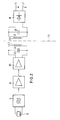
- Fig. 2 shows on the left side the switching elements that are assigned to the read-in device.
- the induction coil 4.1 in the scanning head 4 the inductance of which is designated LS, forms, together with a capacitor CS, an electrical resonant circuit which is connected via a main amplifier V2 and an isolating amplifier V1 to an oscillator G which is controlled by a quartz crystal Q.
- the components CS, V2, V1, G and Q are expediently arranged within the device 6 from FIG. 1. With a correspondingly small training of Switching elements (surface mounted device), the components of the device 6 can be arranged within the optical scanning head 4. Of course, it is also possible to arrange these components within the device 7.
- the resonant circuit LE-CE is connected to a rectifier D, which outputs a DC voltage to a conductor loop at its outputs SP, which can simultaneously be regarded as the feed inputs of the interface of the data memory, the course of which is shown in more detail in FIG. 3.
- Fig. 3 shows a microcomputer CP, which contains a microprocessor and a data memory in a manner not specifically shown.
- the data input is connected to a photodiode PD1, which is arranged in the middle part 3.2 of the transmission head.
- the data output is connected to the base of a transistor T, which lies in the conductor loop a-b, which also contains a resistor R and a luminescent diode LD1 arranged in the middle part 3.2 of the transmitter head.
- the middle part 4.2 of the scanning head 4 opposite the middle part 3.2 of the transmission head can also be seen in FIG. 3 and accordingly contains a photodiode PD2 and a luminescence diode LD2.
- an oscillating signal is generated by the oscillator G after amplification in the amplifiers V1 and V2, it arrives at the decoupling circuit CS, LS and is wirelessly transmitted from the induction coil 4.1 to the induction coil 3.1 and thus the coupling circuit LE-CE.
- the rectifier D emits a DC voltage signal to the conductor loop and thus the operating voltage to the transistor T, via which the data are now read out, which are optically transmitted from the luminescent diode LD1 to the photodiode PD2 and then in a manner not specifically shown in FIG the device 7 arranged evaluation and input units are supplied.
- This type of energy supply for reading out data has the additional advantage that by starting the supply of electrical energy from the outside and thus applying the supply voltage to the transistor T from the rectifier D, the microcomputer CP receives the switch-on signal for reading out the data as " Hardware interrupt "can be given and no special switch-on signal has to be supplied.
- the evaluation and input units arranged in the device 7 of the reading-in device can optically transmit data via the luminescence diode LD2 arranged in the scanning head 4 to the photodiode PD1 arranged in the transmission head 3 and read them into the data memory.
- Fig. 1 data memory 2 and transmitter head 3 are shown as immediately adjacent. This arrangement is by no means mandatory. Since the method described above allows sufficient electrical energy to be supplied from the outside, the data memory 2 and the transmitter head 3 can also be spatially relatively far apart and connected to one another by corresponding lines.
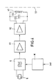
- FIGS. 2 and 3 The addition of the embodiment of FIGS. 2 and 3 is that in the read-in device, the oscillator G is preceded by a modulator M, to which the additional data are supplied via an input "Inf", which the modulator M uses as frequency modulation to output the output signal of the Oscillator G are impressed.
- the receiving side is not shown in FIG. 4.
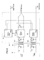
- the circuit parts on the receiving side can be seen in FIG. 5.
- a demodulator DM is connected to the resonant circuit LE-CE, which receives its supply voltage from the DC voltage side of the rectifier D and whose output is connected to a further input of the microcomputer CP.
- the data impressed on the high-frequency signal in the form of frequency modulation are recovered in the demodulator DM and fed to the microcomputer CP for processing.
- the data traffic transmitted by inductive means takes place only on one side, while the data traffic transmitted by optical means runs on both sides.
- two coils, each of which is part of an oscillating circuit only have to be provided both in the transmitting head 3 and in the scanning head 4 in a manner not specifically shown.
- an inductive scanning head 14 is connected in a manner not shown, similar to the optical scanning head 4 of the above-described embodiments, to a transmitter via amplifiers. which emits a high-frequency signal f1 to which data is impressed in the form of frequency modulation. This signal is fed to an induction coil 14.1, which together with a capacitor C1 is part of an electrical resonant circuit and is arranged in the scanning head 14.
- the scanning head 14 contains a second induction coil 14.2, which is arranged in a manner not shown concentrically to the first induction coil 14.1 and together with a capacitor C2 is part of a second electrical resonant circuit which is tuned to a frequency f2 and in a manner not shown with amplifiers is connected to a data receiver.
- This data receiver receives a high-frequency signal with the frequency f2, which is also impressed with data in the form of frequency modulation.
- the two frequencies f1 and f2 are selected differently and can be, for example, 32 kHz and 50 kHz.
- a counter (also not shown in FIG. 6), which has a microprocessor-controlled data memory in an analogous manner to the above-described exemplary embodiments, is connected to an inductive transmission head 13, the interface between the inductive scanning head 14 and your inductive transmission head 13 being spatially approximated is formed by the scanning head and transmission head to achieve a magnetic signal path.
- the transmission head 13 contains a first induction coil 13.1, which together with a capacitor C3 forms part of an oscillating circuit tuned to the frequency f1, which is connected to a rectifier 17, which outputs a DC voltage signal smoothed by a capacitor C5 at its DC voltage outputs, which is used as a supply voltage (CP-SPEISESP.) Is fed to the data memory.
- the rectifier 17 the signal impressed by the induction coil 13.1 is coupled out and fed to a data receiver 15 which also receives its supply voltage from the rectifier 17.
- the data output of the data receiver 15 is connected to a data input (CP-EMPF.DATEN) of the data memory.
- the transmitter head 13 contains a second induction coil 13.2 which, together with a capacitor C4, is part of an electrical resonant circuit which is tuned to the frequency f2 and is connected to a data transmitter 16 which receives its supply voltage from the rectifier 17 and whose data input is connected to a data output (CP-SENDEDATEN) of the data memory is connected.
- a second induction coil 13.2 which, together with a capacitor C4, is part of an electrical resonant circuit which is tuned to the frequency f2 and is connected to a data transmitter 16 which receives its supply voltage from the rectifier 17 and whose data input is connected to a data output (CP-SENDEDATEN) of the data memory is connected.
- the scanning head 14 is arranged by placing it at a corresponding location on a housing (see, for example, FIG. 1) opposite the transmitting head 13 such that the induction coils 14.1 and 13.1 and 14.2 and 13.2 are opposite one another. Electrical energy is supplied via the high-frequency signal with the frequency f1 to generate the supply voltages and to trigger the readout process.
- the data to be read out are fed to the data transmitter 16 and are impressed in a frequency modulation onto the high-frequency signal with the frequency f2, which is then transmitted to the scanning head 14 via the induction coils 13.2 and 14.2 and fed to the receiving devices. If data are to be read into the data memory or test processes are to be triggered, the data which may have been impressed on the high-frequency signal at frequency f1 and which are fed to the data memory via the data receiver 15 are used for this purpose.
- FIG. 7 shows a variant of the embodiment according to FIG. 6, in which the high-frequency signal supplied for supplying the electrical energy for generating the supply voltages is not to be used for data transmission. It then works with three working frequencies f1, f2 and f3.
- the inductive scanning head 24 contains a first induction coil 24.1, which together with the capacitor C6 is part of an oscillating circuit with the frequency f1, a second induction coil 24.2, which together with the capacitor C7 is part of an oscillating circuit with the frequency f2, and a third induction coil 24.3, which is part of a resonant circuit with the frequency f3 with the capacitor C8.
- the induction coils 24.1, 24.2 and 24.3 can be arranged in the scanning head 24 as shown in FIG. 8.
- the three induction coils lie concentrically one inside the other, the outermost induction coil 24.1 being used to transmit the electrical energy used to generate the supply voltage, while the two signal-transmitting induction coils 24.2 and 24.3 are arranged concentrically within this first induction coil.
- the scanning head 24 is connected to the transmitting and receiving devices already mentioned via a cable connection 28.
- the transmitter head 23 contains a first induction coil 23.1, which together with a capacitor C9 forms an oscillating circuit with the frequency f1, a second induction coil 23.2, which together with the capacitor C10 forms an oscillating circuit with the frequency f2, and a third induction coil 23.3, which together with the capacitor C11 forms an oscillating circuit with the frequency f3.
- the first induction coil 23.1 is connected to a rectifier 27, which is smoothed at its DC voltage output by a capacitor C12 Output voltage that is supplied on the one hand to the data memory (CP-SPEISESP.), Not shown, and on the other hand serves to supply a data transmitter 26 and a data receiver 25.
- the data transmitter 26 is connected to the second induction coil 23.2 and the data receiver 25 to the third induction coil 23.3.
- the data input of the data transmitter 26 is connected to a data output (CP-SENDEDATEN) of the data memory, while the data output of the data receiver 25 is connected to a data input (CP-EMPF.DATEN) of the data memory.
- the scanning head 24 is approximated to the transmitting head 23 in the manner already described several times and the corresponding signals are fed in and out via the induction coils 24.1, 24.2, 24.3 and 23.1, 23.2, 23.3.
Landscapes
- Engineering & Computer Science (AREA)
- Physics & Mathematics (AREA)
- General Physics & Mathematics (AREA)
- Computer Networks & Wireless Communication (AREA)
- Signal Processing (AREA)
- Theoretical Computer Science (AREA)
- Arrangements For Transmission Of Measured Signals (AREA)
- Near-Field Transmission Systems (AREA)
Applications Claiming Priority (2)
| Application Number | Priority Date | Filing Date | Title |
|---|---|---|---|
| DE4016010 | 1990-05-18 | ||
| DE4016010A DE4016010A1 (de) | 1990-05-18 | 1990-05-18 | Verfahren zum auslesen und/oder einlesen von daten an einem mikroprozessorgesteuerten datenspeicher, insbesondere eines registrierenden mess- oder zaehlgeraetes sowie einrichtung zur durchfuehrung des verfahrens |
Publications (2)
| Publication Number | Publication Date |
|---|---|
| EP0457306A2 true EP0457306A2 (fr) | 1991-11-21 |
| EP0457306A3 EP0457306A3 (en) | 1992-03-18 |
Family
ID=6406705
Family Applications (1)
| Application Number | Title | Priority Date | Filing Date |
|---|---|---|---|
| EP19910107872 Withdrawn EP0457306A3 (en) | 1990-05-18 | 1991-05-15 | Method and device to read and write a data memory driven by a microprocessor, especially for a measuring or counting recording device |
Country Status (2)
| Country | Link |
|---|---|
| EP (1) | EP0457306A3 (fr) |
| DE (1) | DE4016010A1 (fr) |
Cited By (6)
| Publication number | Priority date | Publication date | Assignee | Title |
|---|---|---|---|---|
| GB2273631A (en) * | 1992-11-25 | 1994-06-22 | Ampy Automation Digilog | Improvements relating to commodity measuring meters |
| WO1995007521A1 (fr) * | 1993-09-11 | 1995-03-16 | Renishaw Plc | Systeme de transmission de signaux pour sondes |
| EP0780822A1 (fr) * | 1995-12-20 | 1997-06-25 | Philips Patentverwaltung GmbH | Méthode et dispositif pour la transmission sans contact de valeurs mesurées |
| EP0825577A1 (fr) * | 1996-08-12 | 1998-02-25 | Laserline SpA | Système de reconnaissance et de lecture à distance de compteurs |
| FR2841066A1 (fr) * | 2002-06-14 | 2003-12-19 | Michaud Sa | Dispositif de transmission d'informations a couplage magnetique |
| EP3227648A1 (fr) * | 2014-12-04 | 2017-10-11 | GWF MessSysteme AG | Compteur et procédé de détermination d'états de compteur et procédé de transmission sans fil d'énergie électrique |
Families Citing this family (2)
| Publication number | Priority date | Publication date | Assignee | Title |
|---|---|---|---|---|
| DE4322811A1 (de) * | 1992-07-08 | 1994-02-10 | Duerrwaechter E Dr Doduco | Einrichtung, insbesondere in Fahrzeugen, zum leitungsgebundenen Übertragen von elektrischen Signalen |
| DE10255741A1 (de) * | 2002-11-28 | 2004-06-09 | Endress + Hauser Conducta Gesellschaft für Mess- und Regeltechnik mbH + Co. KG | Modularer Messumformer mit galvanisch getrennten Messfühler |
Family Cites Families (3)
| Publication number | Priority date | Publication date | Assignee | Title |
|---|---|---|---|---|
| GB2138609A (en) * | 1983-04-19 | 1984-10-24 | Emi Ltd | Electronic counter for mechanical drive |
| DE3613150A1 (de) * | 1986-04-18 | 1987-10-22 | Krupp Gmbh | Vorrichtung zur beruehrungslosen datenuebertragung |
| DE3804592C1 (en) * | 1988-02-13 | 1989-08-03 | Spanner-Pollux Gmbh, 6700 Ludwigshafen, De | Remote read-out system for consumption meter (electricity meter, supply meter) |
-
1990
- 1990-05-18 DE DE4016010A patent/DE4016010A1/de not_active Withdrawn
-
1991
- 1991-05-15 EP EP19910107872 patent/EP0457306A3/de not_active Withdrawn
Cited By (7)
| Publication number | Priority date | Publication date | Assignee | Title |
|---|---|---|---|---|
| GB2273631A (en) * | 1992-11-25 | 1994-06-22 | Ampy Automation Digilog | Improvements relating to commodity measuring meters |
| WO1995007521A1 (fr) * | 1993-09-11 | 1995-03-16 | Renishaw Plc | Systeme de transmission de signaux pour sondes |
| EP0780822A1 (fr) * | 1995-12-20 | 1997-06-25 | Philips Patentverwaltung GmbH | Méthode et dispositif pour la transmission sans contact de valeurs mesurées |
| US5859873A (en) * | 1995-12-20 | 1999-01-12 | U.S. Philips Corporation | Method and arrangement for non-contact transmission of measured values |
| EP0825577A1 (fr) * | 1996-08-12 | 1998-02-25 | Laserline SpA | Système de reconnaissance et de lecture à distance de compteurs |
| FR2841066A1 (fr) * | 2002-06-14 | 2003-12-19 | Michaud Sa | Dispositif de transmission d'informations a couplage magnetique |
| EP3227648A1 (fr) * | 2014-12-04 | 2017-10-11 | GWF MessSysteme AG | Compteur et procédé de détermination d'états de compteur et procédé de transmission sans fil d'énergie électrique |
Also Published As
| Publication number | Publication date |
|---|---|
| EP0457306A3 (en) | 1992-03-18 |
| DE4016010A1 (de) | 1991-11-21 |
Similar Documents
| Publication | Publication Date | Title |
|---|---|---|
| EP0583690B1 (fr) | Carte à puce pourvue d'un détecteur d'intensité de champ | |
| DE4021258C2 (de) | Feldsensor-Kommunikationssystem | |
| DE4002801C1 (fr) | ||
| DE3633939C2 (fr) | ||
| DE3518459C2 (de) | Telemetrie-System | |
| DE60120703T2 (de) | Passiver transponder mit niedrigem energieverbrauch | |
| EP0883097A2 (fr) | Dispositif pour la transmission de signaux entre un émetteur et un récepteur | |
| DE3934007A1 (de) | Zweidraht-fernmesseinrichtung | |
| DE2905734A1 (de) | Elektrooptische datenuebertragungseinrichtung | |
| DE2701184A1 (de) | Schaltungsanordnung zur uebertragung von messwertsignalen | |
| EP1573664B1 (fr) | Dispositif permettant de determiner le niveau d'energie d'un accumulateur d'energie d'un support de donnees mobile | |
| DE10206676A1 (de) | Mit einem Transponder betätigbare Schaltvorrichtung | |
| DE3632840C2 (fr) | ||
| EP0457306A2 (fr) | Procédé et dispositif pour lire et écrire une mémoire de données à microprocesseur, en particulier d'un appareil de comptage ou de mesure d'enregistrement | |
| DE19923634A1 (de) | Sende- und Empfangseinrichtung | |
| DE102004032130B4 (de) | Frequenzsynthesizer und Verfahren zum Betrieb eines Frequenzsynthesizers | |
| DE2439416A1 (de) | Vorrichtung zur ueberwachung der betriebszustaende von maschinenteilen | |
| DE3637689C1 (de) | Faseroptische Messwerterfassungs- und Uebertragungseinrichtung | |
| DE1813319B2 (de) | Vorrichtung zum Erkennen von im Bereich einer Abfrageeinrichtung befindlichen Fahrzeugen | |
| EP0229247A2 (fr) | Dispositif de signalisation sans contact | |
| EP0582257B1 (fr) | Procédé et appareil pour transmettre les informations de signalisation cyclique | |
| EP2508839A1 (fr) | Dispositif de mesure doté d'une commutation d'émission pour la transmission sans fil d'un signal d'émission de valeur de mesure | |
| EP3380852B1 (fr) | Transformateur de mesure de courant inductif | |
| DE69827908T2 (de) | Transponder für berührungslose induktive kommunikation | |
| DE69226803T2 (de) | Positionsmeldevorrichtung eines beweglichen Gliedes |
Legal Events
| Date | Code | Title | Description |
|---|---|---|---|
| PUAI | Public reference made under article 153(3) epc to a published international application that has entered the european phase |
Free format text: ORIGINAL CODE: 0009012 |
|
| AK | Designated contracting states |
Kind code of ref document: A2 Designated state(s): AT BE CH DE DK ES FR GB GR IT LI LU NL SE |
|
| PUAL | Search report despatched |
Free format text: ORIGINAL CODE: 0009013 |
|
| AK | Designated contracting states |
Kind code of ref document: A3 Designated state(s): AT BE CH DE DK ES FR GB GR IT LI LU NL SE |
|
| STAA | Information on the status of an ep patent application or granted ep patent |
Free format text: STATUS: THE APPLICATION IS DEEMED TO BE WITHDRAWN |
|
| 18D | Application deemed to be withdrawn |
Effective date: 19920919 |