EP0457313A1 - Groupe d'assemblage, en particulier pour la technologie des données - Google Patents
Groupe d'assemblage, en particulier pour la technologie des données Download PDFInfo
- Publication number
- EP0457313A1 EP0457313A1 EP19910107887 EP91107887A EP0457313A1 EP 0457313 A1 EP0457313 A1 EP 0457313A1 EP 19910107887 EP19910107887 EP 19910107887 EP 91107887 A EP91107887 A EP 91107887A EP 0457313 A1 EP0457313 A1 EP 0457313A1
- Authority
- EP
- European Patent Office
- Prior art keywords
- printed circuit
- assembly
- circuit board
- sides
- technology
- Prior art date
- Legal status (The legal status is an assumption and is not a legal conclusion. Google has not performed a legal analysis and makes no representation as to the accuracy of the status listed.)
- Granted
Links
Images

Classifications
-
- H—ELECTRICITY
- H10—SEMICONDUCTOR DEVICES; ELECTRIC SOLID-STATE DEVICES NOT OTHERWISE PROVIDED FOR
- H10W—GENERIC PACKAGES, INTERCONNECTIONS, CONNECTORS OR OTHER CONSTRUCTIONAL DETAILS OF DEVICES COVERED BY CLASS H10
- H10W70/00—Package substrates; Interposers; Redistribution layers [RDL]
- H10W70/60—Insulating or insulated package substrates; Interposers; Redistribution layers
- H10W70/611—Insulating or insulated package substrates; Interposers; Redistribution layers for connecting multiple chips together
-
- H—ELECTRICITY
- H05—ELECTRIC TECHNIQUES NOT OTHERWISE PROVIDED FOR
- H05K—PRINTED CIRCUITS; CASINGS OR CONSTRUCTIONAL DETAILS OF ELECTRIC APPARATUS; MANUFACTURE OF ASSEMBLAGES OF ELECTRICAL COMPONENTS
- H05K1/00—Printed circuits
- H05K1/02—Details
- H05K1/14—Structural association of two or more printed circuits
- H05K1/144—Stacked arrangements of planar printed circuit boards
-
- H—ELECTRICITY
- H10—SEMICONDUCTOR DEVICES; ELECTRIC SOLID-STATE DEVICES NOT OTHERWISE PROVIDED FOR
- H10W—GENERIC PACKAGES, INTERCONNECTIONS, CONNECTORS OR OTHER CONSTRUCTIONAL DETAILS OF DEVICES COVERED BY CLASS H10
- H10W90/00—Package configurations
-
- H—ELECTRICITY
- H10—SEMICONDUCTOR DEVICES; ELECTRIC SOLID-STATE DEVICES NOT OTHERWISE PROVIDED FOR
- H10W—GENERIC PACKAGES, INTERCONNECTIONS, CONNECTORS OR OTHER CONSTRUCTIONAL DETAILS OF DEVICES COVERED BY CLASS H10
- H10W90/00—Package configurations
- H10W90/401—Package configurations characterised by multiple insulating or insulated package substrates, interposers or RDLs
Definitions
- the invention relates to an assembly, in particular for data technology equipment.
- the object of the present invention is therefore to create an electrical assembly with an optimal space-power dissipation ratio.
- the assembly is designed in accordance with the invention in such a way that a multilayer printed circuit board, created in the usual lamination technology and provided with multiple potential and signal layers, is connected on both sides via pressure contacts to other printed circuit boards constructed in micro-wiring technology, on the rear sides of which for a predetermined one electrical circuit required, housing-less integrated components (chips) are arranged, which lie directly on the surface of cooling plates.
- a multilayer printed circuit board created in the usual lamination technology and provided with multiple potential and signal layers, is connected on both sides via pressure contacts to other printed circuit boards constructed in micro-wiring technology, on the rear sides of which for a predetermined one electrical circuit required, housing-less integrated components (chips) are arranged, which lie directly on the surface of cooling plates.
- the cooling plates can advantageously be liquid-cooled.
- the potentials can be brought up to the printed circuit board on three sides and the signals on the remaining fourth side.
- a multilayer printed circuit board 1 constructed in the usual lamination technology is arranged in the center of the assembly, which in the present example contains two signal layers inside and four potential layers outside.
- This circuit board 1 is connected via pressure contacts 2 to two further circuit boards, which are constructed using micro-wiring technology, and which have housing-free modules 4 (chips) on their rear side, the chips on their respective upper side directly with cooling plates 5, which are designed as cooling plates through which liquid flows can be contacted.
- the signals and the potentials can be supplied via connector 6 on all four sides of an assembly that is created in this way.
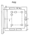
- 2 shows a detailed view of an assembly.
- the printed circuit board 1 protrudes on four sides beyond the printed circuit board, which is built in micro-wiring and carries the building blocks 4.
- potential feeds 8 which can be designed as contact spots, are provided on three sides. These contact spots are over with the respective potential areas inside the circuit board 1 Vias connected.
- the signals from the platter 7 to the signal positions of the printed circuit board 1 and from there also via vias (schematically represented by broken lines 9) to the modules 4 are brought to the printed circuit board 1 via the plug 6.
Landscapes
- Engineering & Computer Science (AREA)
- Microelectronics & Electronic Packaging (AREA)
- Production Of Multi-Layered Print Wiring Board (AREA)
- Combinations Of Printed Boards (AREA)
- Measuring Pulse, Heart Rate, Blood Pressure Or Blood Flow (AREA)
- Accessory Devices And Overall Control Thereof (AREA)
- Coupling Device And Connection With Printed Circuit (AREA)
Applications Claiming Priority (2)
| Application Number | Priority Date | Filing Date | Title |
|---|---|---|---|
| DE4015788A DE4015788C2 (de) | 1990-05-16 | 1990-05-16 | Baugruppe |
| DE4015788 | 1990-05-16 |
Publications (2)
| Publication Number | Publication Date |
|---|---|
| EP0457313A1 true EP0457313A1 (fr) | 1991-11-21 |
| EP0457313B1 EP0457313B1 (fr) | 1996-09-04 |
Family
ID=6406569
Family Applications (1)
| Application Number | Title | Priority Date | Filing Date |
|---|---|---|---|
| EP91107887A Expired - Lifetime EP0457313B1 (fr) | 1990-05-16 | 1991-05-15 | Groupe d'assemblage, en particulier pour la technologie des données |
Country Status (4)
| Country | Link |
|---|---|
| US (1) | US5144532A (fr) |
| EP (1) | EP0457313B1 (fr) |
| AT (1) | ATE142372T1 (fr) |
| DE (2) | DE4015788C2 (fr) |
Cited By (3)
| Publication number | Priority date | Publication date | Assignee | Title |
|---|---|---|---|---|
| EP0506225A3 (en) * | 1991-03-26 | 1993-11-24 | Ibm | Integrated circuit chip package |
| EP0622847A3 (en) * | 1993-04-27 | 1994-11-23 | Ibm | Three dimensional package and architecture for high performance computer. |
| WO1996010265A1 (fr) * | 1994-09-27 | 1996-04-04 | Foster-Miller, Inc. | Technique d'encapsulage de puces |
Families Citing this family (22)
| Publication number | Priority date | Publication date | Assignee | Title |
|---|---|---|---|---|
| JP2550798Y2 (ja) * | 1992-04-11 | 1997-10-15 | 株式会社デンソー | 混成集積回路装置 |
| US5854534A (en) | 1992-08-05 | 1998-12-29 | Fujitsu Limited | Controlled impedence interposer substrate |
| JP2611671B2 (ja) * | 1994-07-26 | 1997-05-21 | 日本電気株式会社 | 半導体装置 |
| US6333849B1 (en) | 1996-07-01 | 2001-12-25 | Compaq Computer Corporation | Apparatus for liquid cooling of specific computer components |
| US6236901B1 (en) * | 1998-03-31 | 2001-05-22 | Dell Usa, L.P. | Manufacturing system and method for assembly of computer systems in a build-to-order environment |
| US6631606B2 (en) * | 2000-01-18 | 2003-10-14 | Dell Products L.P. | System and method for accommodating atypical customer requirements in a mass customization manufacturing facility |
| US6892104B2 (en) * | 2000-01-18 | 2005-05-10 | Dell Products L.P. | System and method for manufacturing products according to customer orders |
| US6516242B1 (en) | 2000-01-18 | 2003-02-04 | Dell Usa, L.P. | Apparatus for consolidating manufacturing of computing devices |
| US6711798B2 (en) | 2000-01-18 | 2004-03-30 | Dell Products L.P. | Method for manufacturing products according to customer orders |
| US7149884B2 (en) | 2001-01-25 | 2006-12-12 | Dell Products L.P. | Method and system for configuring a computer system via a wireless communication link |
| US6529797B2 (en) | 2001-03-05 | 2003-03-04 | Dell Products L.P. | System and method for automatically releasing collections of goods for shipment |
| US6505094B2 (en) | 2001-03-05 | 2003-01-07 | Dell Products L.P. | System and method for shipping items from a distribution facility |
| US6634506B2 (en) | 2001-03-05 | 2003-10-21 | Dell Products L.P. | Reusable container management system and method |
| US6611727B2 (en) | 2001-03-05 | 2003-08-26 | Dell Products L.P. | Method and system for simulating production within a manufacturing environment |
| US6816746B2 (en) | 2001-03-05 | 2004-11-09 | Dell Products L.P. | Method and system for monitoring resources within a manufacturing environment |
| US6560509B2 (en) | 2001-03-05 | 2003-05-06 | Dell Products L.P. | System and method for automated management of a distribution facility |
| US20020123918A1 (en) * | 2001-03-05 | 2002-09-05 | Dell Products L.P. | System and method for manufacturing and shipping products according to customer orders |
| US6615092B2 (en) | 2001-03-05 | 2003-09-02 | Dell Products L.P. | Method, system and facility for controlling resource allocation within a manufacturing environment |
| US6962306B2 (en) * | 2002-07-15 | 2005-11-08 | West Ronald R | Units for storing flexible elongated objects |
| US7193854B2 (en) * | 2005-05-02 | 2007-03-20 | Verigy Pte. Ltd | Using a leaf spring to attach clamp plates with a heat sink to both sides of a component mounted on a printed circuit assembly |
| TWM296550U (en) * | 2006-01-11 | 2006-08-21 | Delta Electronics Inc | Ethernet component |
| CN116093688B (zh) * | 2023-01-29 | 2025-12-02 | 绿色点子创意开发有限公司 | 配重式转接插座构造 |
Citations (4)
| Publication number | Priority date | Publication date | Assignee | Title |
|---|---|---|---|---|
| US4283754A (en) * | 1979-03-26 | 1981-08-11 | Bunker Ramo Corporation | Cooling system for multiwafer high density circuit |
| US4771366A (en) * | 1987-07-06 | 1988-09-13 | International Business Machines Corporation | Ceramic card assembly having enhanced power distribution and cooling |
| US4868712A (en) * | 1987-02-04 | 1989-09-19 | Woodman John K | Three dimensional integrated circuit package |
| EP0332747A2 (fr) * | 1988-03-14 | 1989-09-20 | International Business Machines Corporation | Empaquetage à montage automatique sur bande |
Family Cites Families (14)
| Publication number | Priority date | Publication date | Assignee | Title |
|---|---|---|---|---|
| US3253246A (en) * | 1963-07-30 | 1966-05-24 | Ibm | Printed circuit card connector |
| US3766439A (en) * | 1972-01-12 | 1973-10-16 | Gen Electric | Electronic module using flexible printed circuit board with heat sink means |
| US4016463A (en) * | 1973-10-17 | 1977-04-05 | Amdahl Corporation | High density multilayer printed circuit card assembly and method |
| DE3321321A1 (de) * | 1982-06-19 | 1983-12-22 | Ferranti plc, Gatley, Cheadle, Cheshire | Elektrische schaltungsanordnung |
| ATE39788T1 (de) * | 1982-09-09 | 1989-01-15 | Siemens Ag | Einrichtung zum kuehlen einer mehrzahl von zu flachbaugruppen zusammengefassten integrierten bausteinen. |
| GB2129223A (en) * | 1982-10-09 | 1984-05-10 | Welwyn Electronics Ltd | Printed circuit boards |
| CA1229155A (fr) * | 1983-03-29 | 1987-11-10 | Toshihiko Watari | Progiciel lsi a grande densite pour circuite logiques |
| US4581679A (en) * | 1983-05-31 | 1986-04-08 | Trw Inc. | Multi-element circuit construction |
| DE3536963A1 (de) * | 1985-10-17 | 1987-04-23 | Diehl Gmbh & Co | Baugruppenanordnung |
| US4774632A (en) * | 1987-07-06 | 1988-09-27 | General Electric Company | Hybrid integrated circuit chip package |
| JPS6457789A (en) * | 1987-08-28 | 1989-03-06 | Mitsubishi Electric Corp | Electronic component mounting structure |
| EP0320198B1 (fr) * | 1987-12-07 | 1995-03-01 | Nec Corporation | Système de refroidissement pour l'empaquetage d'un circuit intégré |
| FR2625042B1 (fr) * | 1987-12-22 | 1990-04-20 | Thomson Csf | Structure microelectronique hybride modulaire a haute densite d'integration |
| US4939624A (en) * | 1988-12-14 | 1990-07-03 | Cray Research, Inc. | Interconnected multiple circuit module |
-
1990
- 1990-05-16 DE DE4015788A patent/DE4015788C2/de not_active Expired - Fee Related
-
1991
- 1991-05-15 US US07/700,502 patent/US5144532A/en not_active Expired - Fee Related
- 1991-05-15 EP EP91107887A patent/EP0457313B1/fr not_active Expired - Lifetime
- 1991-05-15 AT AT91107887T patent/ATE142372T1/de active
- 1991-05-15 DE DE59108131T patent/DE59108131D1/de not_active Expired - Fee Related
Patent Citations (4)
| Publication number | Priority date | Publication date | Assignee | Title |
|---|---|---|---|---|
| US4283754A (en) * | 1979-03-26 | 1981-08-11 | Bunker Ramo Corporation | Cooling system for multiwafer high density circuit |
| US4868712A (en) * | 1987-02-04 | 1989-09-19 | Woodman John K | Three dimensional integrated circuit package |
| US4771366A (en) * | 1987-07-06 | 1988-09-13 | International Business Machines Corporation | Ceramic card assembly having enhanced power distribution and cooling |
| EP0332747A2 (fr) * | 1988-03-14 | 1989-09-20 | International Business Machines Corporation | Empaquetage à montage automatique sur bande |
Non-Patent Citations (1)
| Title |
|---|
| IBM TECHNICAL DISCLOSURE BULLETIN, Band 19, Nr. 4, September 1976, Seiten 1270-1271, New York, US; Z. MARKEWYCZ: "Distribution system for multilayer ceramic modules" * |
Cited By (6)
| Publication number | Priority date | Publication date | Assignee | Title |
|---|---|---|---|---|
| EP0506225A3 (en) * | 1991-03-26 | 1993-11-24 | Ibm | Integrated circuit chip package |
| EP0622847A3 (en) * | 1993-04-27 | 1994-11-23 | Ibm | Three dimensional package and architecture for high performance computer. |
| US5495397A (en) * | 1993-04-27 | 1996-02-27 | International Business Machines Corporation | Three dimensional package and architecture for high performance computer |
| US5817986A (en) * | 1993-04-27 | 1998-10-06 | International Business Machines Corporation | Three dimensional package and architecture for high performance computer |
| WO1996010265A1 (fr) * | 1994-09-27 | 1996-04-04 | Foster-Miller, Inc. | Technique d'encapsulage de puces |
| US6320257B1 (en) | 1994-09-27 | 2001-11-20 | Foster-Miller, Inc. | Chip packaging technique |
Also Published As
| Publication number | Publication date |
|---|---|
| US5144532A (en) | 1992-09-01 |
| EP0457313B1 (fr) | 1996-09-04 |
| DE4015788A1 (de) | 1991-11-21 |
| DE4015788C2 (de) | 1994-06-23 |
| DE59108131D1 (de) | 1996-10-10 |
| ATE142372T1 (de) | 1996-09-15 |
Similar Documents
| Publication | Publication Date | Title |
|---|---|---|
| EP0457313B1 (fr) | Groupe d'assemblage, en particulier pour la technologie des données | |
| DE1591199C2 (fr) | ||
| DE69800514T2 (de) | Leiterplatte mit primären und sekundären Durchgangslöchern | |
| AT398254B (de) | Chipträger sowie anordnung von solchen chipträgern | |
| DE69200500T2 (de) | Gestufte Mehrlagenverbindungsplatte und Herstellungsmethoden. | |
| DE2362939A1 (de) | Raumsparende zusammenschaltungs- und zusammenbauanordnung fuer komplexe digitalsysteme und verfahren zu ihrer herstellung | |
| DE3852420T2 (de) | Elektrische Kodierung für ersetzbare Module. | |
| DE3026183A1 (de) | Gehaeuse fuer integrierte logikschaltkreise | |
| DE1591199B1 (de) | Schaltungsanordnung fuer elektronische Schaltungen | |
| DE102008023451A1 (de) | Elektrische Verbindungsanordnung | |
| EP0471982B1 (fr) | Système de montage pour unités électriques de fonction, notamment pour la technique de données | |
| DE3879737T2 (de) | Steckbares Gehäuse integrierter Schaltungen. | |
| EP0106990A1 (fr) | Elément pour faire contact entre des plaquettes à circuit imprimé | |
| DE1942839A1 (de) | Steckbare Platte mit gedruckter Schaltung | |
| EP0166027B1 (fr) | Cellule élémentaire réalisée en technique C-MOS | |
| DE10249205B3 (de) | Leistungsbauelementanordnung zur mechatronischen Integration von Leistungsbauelementen | |
| EP0428859B1 (fr) | Unité fonctionnelle électrique pour traitement de données | |
| DE112005002373T5 (de) | Geteilter Dünnschichtkondensator für mehrere Spannungen | |
| DE2810575A1 (de) | Gedruckte elektrische schaltungsplatte | |
| DE3330466A1 (de) | Anordnung mit hoher packungsdichte von integrierten schaltungen | |
| EP0238915B1 (fr) | Ensemble de connexion et de circuit | |
| DE60201537T2 (de) | Elektrische verbindungsanordnung für elektronische bauteile | |
| DE2742534A1 (de) | Verbindungselement fuer elektronische schaltungen | |
| DE3411707A1 (de) | Rueckwandverdrahtung fuer einschiebbare elektrische baugruppen | |
| DE3435773A1 (de) | Rueckwandverdrahtung fuer einschiebbare elektrische baugruppen |
Legal Events
| Date | Code | Title | Description |
|---|---|---|---|
| PUAI | Public reference made under article 153(3) epc to a published international application that has entered the european phase |
Free format text: ORIGINAL CODE: 0009012 |
|
| AK | Designated contracting states |
Kind code of ref document: A1 Designated state(s): AT BE CH DE FR GB IT LI NL |
|
| 17P | Request for examination filed |
Effective date: 19911206 |
|
| RAP3 | Party data changed (applicant data changed or rights of an application transferred) |
Owner name: SIEMENS NIXDORF INFORMATIONSSYSTEME AG |
|
| 17Q | First examination report despatched |
Effective date: 19940608 |
|
| GRAH | Despatch of communication of intention to grant a patent |
Free format text: ORIGINAL CODE: EPIDOS IGRA |
|
| GRAA | (expected) grant |
Free format text: ORIGINAL CODE: 0009210 |
|
| AK | Designated contracting states |
Kind code of ref document: B1 Designated state(s): AT BE CH DE FR GB IT LI NL |
|
| PG25 | Lapsed in a contracting state [announced via postgrant information from national office to epo] |
Ref country code: IT Free format text: LAPSE BECAUSE OF FAILURE TO SUBMIT A TRANSLATION OF THE DESCRIPTION OR TO PAY THE FEE WITHIN THE PRE;WARNING: LAPSES OF ITALIAN PATENTS WITH EFFECTIVE DATE BEFORE 2007 MAY HAVE OCCURRED AT ANY TIME BEFORE 2007. THE CORRECT EFFECTIVE DATE MAY BE DIFFERENT FROM THE ONE RECORDED.SCRIBED TIME-LIMIT Effective date: 19960904 Ref country code: NL Free format text: LAPSE BECAUSE OF FAILURE TO SUBMIT A TRANSLATION OF THE DESCRIPTION OR TO PAY THE FEE WITHIN THE PRESCRIBED TIME-LIMIT Effective date: 19960904 Ref country code: FR Effective date: 19960904 Ref country code: GB Effective date: 19960904 |
|
| REF | Corresponds to: |
Ref document number: 142372 Country of ref document: AT Date of ref document: 19960915 Kind code of ref document: T |
|
| REF | Corresponds to: |
Ref document number: 59108131 Country of ref document: DE Date of ref document: 19961010 |
|
| EN | Fr: translation not filed | ||
| NLV1 | Nl: lapsed or annulled due to failure to fulfill the requirements of art. 29p and 29m of the patents act | ||
| GBV | Gb: ep patent (uk) treated as always having been void in accordance with gb section 77(7)/1977 [no translation filed] |
Effective date: 19960904 |
|
| PG25 | Lapsed in a contracting state [announced via postgrant information from national office to epo] |
Ref country code: AT Free format text: LAPSE BECAUSE OF NON-PAYMENT OF DUE FEES Effective date: 19970515 |
|
| PG25 | Lapsed in a contracting state [announced via postgrant information from national office to epo] |
Ref country code: BE Effective date: 19970531 Ref country code: CH Free format text: LAPSE BECAUSE OF NON-PAYMENT OF DUE FEES Effective date: 19970531 Ref country code: LI Free format text: LAPSE BECAUSE OF NON-PAYMENT OF DUE FEES Effective date: 19970531 |
|
| PLBE | No opposition filed within time limit |
Free format text: ORIGINAL CODE: 0009261 |
|
| STAA | Information on the status of an ep patent application or granted ep patent |
Free format text: STATUS: NO OPPOSITION FILED WITHIN TIME LIMIT |
|
| 26N | No opposition filed | ||
| BERE | Be: lapsed |
Owner name: SIEMENS NIXDORF INFORMATIONSSYSTEME A.G. Effective date: 19970531 |
|
| REG | Reference to a national code |
Ref country code: CH Ref legal event code: PL |
|
| PG25 | Lapsed in a contracting state [announced via postgrant information from national office to epo] |
Ref country code: DE Free format text: LAPSE BECAUSE OF NON-PAYMENT OF DUE FEES Effective date: 19980203 |