EP0457577A1 - Photosensitive imaging member with a low-reflection ground plane - Google Patents
Photosensitive imaging member with a low-reflection ground plane Download PDFInfo
- Publication number
- EP0457577A1 EP0457577A1 EP91304375A EP91304375A EP0457577A1 EP 0457577 A1 EP0457577 A1 EP 0457577A1 EP 91304375 A EP91304375 A EP 91304375A EP 91304375 A EP91304375 A EP 91304375A EP 0457577 A1 EP0457577 A1 EP 0457577A1
- Authority
- EP
- European Patent Office
- Prior art keywords
- ground plane
- imaging member
- layer
- dielectric substrate
- light
- Prior art date
- Legal status (The legal status is an assumption and is not a legal conclusion. Google has not performed a legal analysis and makes no representation as to the accuracy of the status listed.)
- Granted
Links
Images


Classifications
-
- G—PHYSICS
- G03—PHOTOGRAPHY; CINEMATOGRAPHY; ANALOGOUS TECHNIQUES USING WAVES OTHER THAN OPTICAL WAVES; ELECTROGRAPHY; HOLOGRAPHY
- G03G—ELECTROGRAPHY; ELECTROPHOTOGRAPHY; MAGNETOGRAPHY
- G03G5/00—Recording-members for original recording by exposure, e.g. to light, to heat or to electrons; Manufacture thereof; Selection of materials therefor
- G03G5/10—Bases for charge-receiving or other layers
- G03G5/104—Bases for charge-receiving or other layers comprising inorganic material other than metals, e.g. salts, oxides, carbon
-
- G—PHYSICS
- G03—PHOTOGRAPHY; CINEMATOGRAPHY; ANALOGOUS TECHNIQUES USING WAVES OTHER THAN OPTICAL WAVES; ELECTROGRAPHY; HOLOGRAPHY
- G03G—ELECTROGRAPHY; ELECTROPHOTOGRAPHY; MAGNETOGRAPHY
- G03G5/00—Recording-members for original recording by exposure, e.g. to light, to heat or to electrons; Manufacture thereof; Selection of materials therefor
- G03G5/02—Charge-receiving layers
- G03G5/04—Photoconductive layers; Charge-generation layers or charge-transporting layers; Additives therefor; Binders therefor
- G03G5/043—Photoconductive layers characterised by having two or more layers or characterised by their composite structure
- G03G5/047—Photoconductive layers characterised by having two or more layers or characterised by their composite structure characterised by the charge-generation layers or charge transport layers
-
- G—PHYSICS
- G03—PHOTOGRAPHY; CINEMATOGRAPHY; ANALOGOUS TECHNIQUES USING WAVES OTHER THAN OPTICAL WAVES; ELECTROGRAPHY; HOLOGRAPHY
- G03G—ELECTROGRAPHY; ELECTROPHOTOGRAPHY; MAGNETOGRAPHY
- G03G5/00—Recording-members for original recording by exposure, e.g. to light, to heat or to electrons; Manufacture thereof; Selection of materials therefor
- G03G5/10—Bases for charge-receiving or other layers
Definitions
- the present invention relates to an imaging systems of the type using coherent light radiation to expose a photosensitive imaging member.
- a coherent beam of radiation typically from a helium-neon or diode laser is modulated by an input image data signal.
- the modulated beam is directed (scanned) across the surface of a photosensitive medium.
- the medium can be, for example, a photoreceptor drum or belt in a xerographic printer, a photosensor CCD array, or a photosensitive film.
- Certain classes of photosensitive medium which can be characterized as "layered photoreceptors" have at least a partially transparent photosensitive layer overlying a conductive ground plane.
- This condition is shown in Figure 1; coherent beams 1 and 2 are incident on a layered photoreceptor 6 comprising a charge transport layer 7, charge generator layer 8, and a ground plane 9.
- the two dominant reflections are: from the top surface of layer 7, and from the top surface of ground plane 9.
- beams 1 and 2 can interfere constructively or destructively when they combine to form beam 3.
- Figure 2 shows the areas of spatial exposure variation (at 25x) within a photoreceptor of the type shown in Figure 1 when illuminated by a He-Ne laser with an output wavelength of 633 nm.
- the pattern of light and dark interference fringes look like the grains on a sheet of plywood.
- the term "plywood effect" is generically applied to this problem.
- One method of compensating for the plywood effect known to the prior art is to increase the thickness of and, hence, the absorption of the light by the charge generator layer. For most systems, this leads to unacceptable tradeoffs; for example, for a layered organic photoreceptor, an increase in dark decay characteristics and electrical cyclic instability may occur.
- Another method, disclosed in U.S. Patent 4,618,552 is to use a photoconductive imaging member in which the ground plane, or an opaque conductive layer formed above or below the ground plane, is formed with a rough surface morphology to diffusely reflect the light.
- the plywood effect is significantly reduced by suppressing the interference fringes produced by strong reflections from the conductive substrate.
- This is accomplished by replacing the present ground plane by a conductive transparent low-reflectivity ground plane.
- an electrically inactive absorbing layer is added to the back of the substrate upon which the ground plane is formed.
- the invention relates to a photosensitive imaging member comprising at least a transparent photoconductive charge transport layer, overlying a charge generator layer and a conductive ground plane characterized by said ground plane being of a transparent and low-reflection material.
- Figure 1 shows coherent light incident upon a prior art layered photosensitive medium leading to reflections internal to the medium.
- Figure 2 shows a spatial exposure variation plywood pattern in the exposed photosensitive medium of Figure 1 produced when the spatial variation in the absorption within the photosensitive member occurs due to an interference effect.
- Figure 3 is a schematic representation of an optical system incorporating a coherent light source to scan a light beam across a photoreceptor.
- Figure 4 is a cross-sectional view of the photoreceptor of Figure 3.
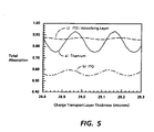
- Figure 5 is a plot of total absorption versus transport layer thickness for a ground plane as shown in Figure 4 comprising a) conventional ground plane comprising titanium, b) an indium tin oxide (ITO) ground plane, and c) a combination of an ITO ground plane with an absorbing anti-curl layer.
- a ground plane as shown in Figure 4 comprising a) conventional ground plane comprising titanium, b) an indium tin oxide (ITO) ground plane, and c) a combination of an ITO ground plane with an absorbing anti-curl layer.
- ITO indium tin oxide
- FIG 3 shows an imaging system 10 wherein a laser 12 produces a coherent output which is scanned across photoreceptor 14.
- the laser diode is driven so as to provide a modulated light output beam 16.
- Flat field collector and objective lens 18 and 20, respectively, are positioned in the optical path between laser 12 and light beam reflecting scanning device 22.
- device 22 is a multi-faceted mirror polygon driven by motor 23, as shown.
- Flat field collector lens 18 collimates the diverging light beam 16 and field objective lens 20 causes the collected beam to be focused onto photoreceptor 14 after reflection from polygon 22.
- Photoreceptor 14 is a layered photoreceptor shown in partial cross-section in Figure 4.
- photoreceptor 14 is a layered photoreceptor which includes a transparent conductive ground plane 32 formed on a dielectric substrate 34 (typically polyethylene terephthalate (PET)).
- substrate 34 typically polyethylene terephthalate (PET)
- Substrate 34 has, as is conventional, a anti-curl coating 35 on the bottom surface thereof.
- ground plane 32 has formed thereon a polysilane layer 36 whose function is to act as a blocking layer.
- layer 38 whose function is to act as an adhesion layer.
- Charge generator layer 40 and charge transport layer 42 are conventionally formed according to the teachings of U.S. Patent 4,588,667. Layers 36, 38, 40, and 42 are all transparent to incident light and have approximately the same refractive index.
- Conductive ground plane 32 is a transparent and low refractive index conductor.
- ground plane 32 is indium tin oxide with a refractive index of 1.9.
- the indium tin oxide is preferentially formed to a thickness of some multiple of the incident wavelength.
- laser source 12 is a helium-neon laser
- output beam 16 has a wavelength ⁇ of 632.8 nm.
- the 4% reflection from the anti-curl layer air interface is eliminated by adding selected dye materials either to the PET substrate 34 or the anti-curl layer 35 to absorb the light reflected from the interface.
- selected dye materials either to the PET substrate 34 or the anti-curl layer 35 to absorb the light reflected from the interface.
- One example of a suitable dye material is Sudan Blue 670 TM .
- the exact degree of absorption to be accomplished depends on the system requirements. For some systems using a charge erase directed from the back of the photoreceptor (upward through anti-curl layer 35) there may be some trade-off in reducing the absorbing proportion of the anti-curl layer to allow for sufficient light transmission to effect discharge at the ground plane.
- Figure 5 shows a plot of the total absorption of the incident light within the photoreceptor as a function of the charge transport layer thickness.
- a low-reflection ground plane comprising indium tin oxide both with and without an absorbing anti-curl layer and, also shown for comparison purposes, a conventional opaque titanium ground plane.
- the absorption is plotted against transport layer thickness, the modulation in the absorption correlates directly to the interference fringe contrast with larger magnitude modulations signifying strong plywood fringe contrast in the final print. Conversely, small magnitude modulation results in weak plywood fringe contrast in the final print.
- plot c ITO used with an absorbing layer
- plot b ITO layer alone
- Other acceptable low-reflection materials for the ground plane can be tin oxide or silver halide salt materials.
- the optimum thickness of the ITO ground plane sandwiched between materials having nearly the same refractive index as in the photoreceptor structure is k ⁇ /2n, where k is an integer, ⁇ is the light wavelength for exposure of the photoreceptor and n is the refractive index.
- Other thicknesses for the ITO will have a higher reflectivity and thus are not optimum.
- Even non-optimum thickness for the ITO have lower reflectivity than conventional ground planes and consequently substantially reduced plywood.
- the ITO thickness having maximum reflectivity, ⁇ /4n will have a reflectivity less than 10%.
Landscapes
- Physics & Mathematics (AREA)
- General Physics & Mathematics (AREA)
- Chemical & Material Sciences (AREA)
- Inorganic Chemistry (AREA)
- Photoreceptors In Electrophotography (AREA)
- Surface Treatment Of Optical Elements (AREA)
- Transforming Light Signals Into Electric Signals (AREA)
Abstract
Description
- The present invention relates to an imaging systems of the type using coherent light radiation to expose a photosensitive imaging member.
- There are numerous applications in the electrophotographic art wherein a coherent beam of radiation, typically from a helium-neon or diode laser is modulated by an input image data signal. The modulated beam is directed (scanned) across the surface of a photosensitive medium. The medium can be, for example, a photoreceptor drum or belt in a xerographic printer, a photosensor CCD array, or a photosensitive film. Certain classes of photosensitive medium which can be characterized as "layered photoreceptors" have at least a partially transparent photosensitive layer overlying a conductive ground plane. A problem inherent in using these layered photoreceptors, depending upon the physical characteristics, is the creation of two dominant reflections of the incident coherent light on the surface of the photoreceptor; e.g., a first reflection from the top surface and a second reflection from the top surface of the relatively opaque conductive ground plane. This condition is shown in Figure 1;
coherent beams layered photoreceptor 6 comprising a charge transport layer 7,charge generator layer 8, and aground plane 9. The two dominant reflections are: from the top surface of layer 7, and from the top surface ofground plane 9. Depending on the optical path difference as determined by the thickness and index of refraction of layer 7,beams beam 3. When the additional optical path traveled by beam 1 (dashed rays) is an integer multiple of the wavelength of the light, constructive interference occurs, more light is reflected from the top of charge transport layer 7 and, hence, less light is absorbed bycharge generator layer 8. Conversely, a path difference producing destructive interference means less light is lost out of the layer and more absorption occurs within thecharge generator layer 8. The difference in absorption in thecharge generator layer 8, typically due to layer thickness variations within the charge transport layer 7, is equivalent to a spatial variation in exposure on the surface. This spatial exposure variation present in the image formed on the photoreceptor becomes manifest in the output copy derived from the exposed photoreceptor. Figure 2 shows the areas of spatial exposure variation (at 25x) within a photoreceptor of the type shown in Figure 1 when illuminated by a He-Ne laser with an output wavelength of 633 nm. The pattern of light and dark interference fringes look like the grains on a sheet of plywood. Hence the term "plywood effect" is generically applied to this problem. - One method of compensating for the plywood effect known to the prior art is to increase the thickness of and, hence, the absorption of the light by the charge generator layer. For most systems, this leads to unacceptable tradeoffs; for example, for a layered organic photoreceptor, an increase in dark decay characteristics and electrical cyclic instability may occur. Another method, disclosed in U.S. Patent 4,618,552 is to use a photoconductive imaging member in which the ground plane, or an opaque conductive layer formed above or below the ground plane, is formed with a rough surface morphology to diffusely reflect the light.
- According to the present invention the plywood effect is significantly reduced by suppressing the interference fringes produced by strong reflections from the conductive substrate. This is accomplished by replacing the present ground plane by a conductive transparent low-reflectivity ground plane. In a further embodiment, an electrically inactive absorbing layer is added to the back of the substrate upon which the ground plane is formed. More particularly, the invention relates to a photosensitive imaging member comprising at least a transparent photoconductive charge transport layer, overlying a charge generator layer and a conductive ground plane characterized by said ground plane being of a transparent and low-reflection material.
- Figure 1 shows coherent light incident upon a prior art layered photosensitive medium leading to reflections internal to the medium.
- Figure 2 shows a spatial exposure variation plywood pattern in the exposed photosensitive medium of Figure 1 produced when the spatial variation in the absorption within the photosensitive member occurs due to an interference effect.
- Figure 3 is a schematic representation of an optical system incorporating a coherent light source to scan a light beam across a photoreceptor.
- Figure 4 is a cross-sectional view of the photoreceptor of Figure 3.
- Figure 5 is a plot of total absorption versus transport layer thickness for a ground plane as shown in Figure 4 comprising a) conventional ground plane comprising titanium, b) an indium tin oxide (ITO) ground plane, and c) a combination of an ITO ground plane with an absorbing anti-curl layer.
- Figure 3 shows an
imaging system 10 wherein alaser 12 produces a coherent output which is scanned acrossphotoreceptor 14. In response to video signal information representing the information to be printed or copied, the laser diode is driven so as to provide a modulatedlight output beam 16. Flat field collector andobjective lens laser 12 and light beam reflectingscanning device 22. In a preferred embodiment,device 22 is a multi-faceted mirror polygon driven bymotor 23, as shown. Flatfield collector lens 18 collimates the diverginglight beam 16 and fieldobjective lens 20 causes the collected beam to be focused ontophotoreceptor 14 after reflection frompolygon 22.Photoreceptor 14 is a layered photoreceptor shown in partial cross-section in Figure 4. - Referring to Figure 4,
photoreceptor 14 is a layered photoreceptor which includes a transparentconductive ground plane 32 formed on a dielectric substrate 34 (typically polyethylene terephthalate (PET)).Substrate 34 has, as is conventional, aanti-curl coating 35 on the bottom surface thereof. As is conventional in the art,ground plane 32 has formed thereon apolysilane layer 36 whose function is to act as a blocking layer. Formed on top ofblocking layer 36 islayer 38 whose function is to act as an adhesion layer.Charge generator layer 40 andcharge transport layer 42 are conventionally formed according to the teachings of U.S. Patent 4,588,667.Layers -
Conductive ground plane 32 is a transparent and low refractive index conductor. In a preferred form,ground plane 32 is indium tin oxide with a refractive index of 1.9. - The indium tin oxide is preferentially formed to a thickness of some multiple of the incident wavelength. Thus, for example, if
laser source 12 is a helium-neon laser,output beam 16 has a wavelength λ of 632.8 nm. At 1/2 wavelength thickness,ground plane 34 will be λ/2n thick. If n = 1.9 and λ = 632.8 nm, theground plane 34 will be approximately 0.167f microns or 167f nm thick. At this 1/2 wavelength optical thickness value, little, of the light passing through the layers overlyingground plane 34 is reflected; e.g., the light is transmitted through the ground plane. Thus, the only relatively strong reflections which serve to form an undesirable spatial variation exposure at the surface oflayer 42 are the approximately 4% reflection from that surface and an additional approximately 4% reflection at the air/anti-curl layer 35 interface. This embodiment thus effectively eliminates the type of exposure variation pattern shown in Figure 2. Output prints exhibit virtually no plywood effect defects. - According to a modification, the 4% reflection from the anti-curl layer air interface is eliminated by adding selected dye materials either to the
PET substrate 34 or theanti-curl layer 35 to absorb the light reflected from the interface. One example of a suitable dye material is Sudan Blue 670TM. The exact degree of absorption to be accomplished depends on the system requirements. For some systems using a charge erase directed from the back of the photoreceptor (upward through anti-curl layer 35) there may be some trade-off in reducing the absorbing proportion of the anti-curl layer to allow for sufficient light transmission to effect discharge at the ground plane. - Figure 5 shows a plot of the total absorption of the incident light within the photoreceptor as a function of the charge transport layer thickness. Three cases are shown: a low-reflection ground plane comprising indium tin oxide both with and without an absorbing anti-curl layer and, also shown for comparison purposes, a conventional opaque titanium ground plane. The absorption is plotted against transport layer thickness, the modulation in the absorption correlates directly to the interference fringe contrast with larger magnitude modulations signifying strong plywood fringe contrast in the final print. Conversely, small magnitude modulation results in weak plywood fringe contrast in the final print. Thus, plot c (ITO used with an absorbing layer) is more preferable than plot b (ITO layer alone) which is in turn more preferable to the titanium ground plane, (plot a). Other acceptable low-reflection materials for the ground plane can be tin oxide or silver halide salt materials.
- The optimum thickness of the ITO ground plane sandwiched between materials having nearly the same refractive index as in the photoreceptor structure is kλ/2n, where k is an integer, λ is the light wavelength for exposure of the photoreceptor and n is the refractive index. Other thicknesses for the ITO will have a higher reflectivity and thus are not optimum. Even non-optimum thickness for the ITO have lower reflectivity than conventional ground planes and consequently substantially reduced plywood. For instance, the ITO thickness having maximum reflectivity, λ/4n, will have a reflectivity less than 10%.
Claims (7)
- A photosensitive imaging member adapted to be exposed by radiation from a coherent light source, said member comprising at least a transparent photoconductive charge transport layer (42), overlying a charge generator layer (40) and a conductive ground plane (32), said ground plane comprising a transparent low-reflection material.
- An imaging member as claimed in Claim 1, wherein said charge transport layer, charge generator layer and ground plane have approximately the same index of refraction, and wherein said ground plane has a thickness given by the expression t = k λ/2n where k is an integer and n is the wavelength of the incident light.
- An imaging member as claimed in Claim 2, wherein the thickness of the ground plane is given by the expression t = k λ/4n
- An imaging member as claimed in any one of the preceding Claims, wherein said ground plane is formed of indium tin oxide.
- An imaging member as claimed in any one of the preceding Claims, further including a dielectric substrate supporting said ground plane, said dielectric substrate being adapted to absorb radiation reflected from the interface between said substrate and air.
- An imaging member as claimed in Claim 5, wherein said dielectric substrate comprises a dielectric substrate layer with an anti-curl coating (35) on the bottom surface, the anti-curl coating being adapted to absorb light reflected from the anti-curl layer/air interface.
- A raster output scanning system comprising an imaging member (14) as claimed in any one of the preceding claims;
means (12) for generating a beam of high intensity, modulated coherent light, and optical means (18, 20, 22) for imaging said beam onto the surface of the imaging member.
Applications Claiming Priority (2)
| Application Number | Priority Date | Filing Date | Title |
|---|---|---|---|
| US523639 | 1990-05-15 | ||
| US07/523,639 US5051328A (en) | 1990-05-15 | 1990-05-15 | Photosensitive imaging member with a low-reflection ground plane |
Publications (2)
| Publication Number | Publication Date |
|---|---|
| EP0457577A1 true EP0457577A1 (en) | 1991-11-21 |
| EP0457577B1 EP0457577B1 (en) | 1995-08-09 |
Family
ID=24085813
Family Applications (1)
| Application Number | Title | Priority Date | Filing Date |
|---|---|---|---|
| EP91304375A Expired - Lifetime EP0457577B1 (en) | 1990-05-15 | 1991-05-15 | Photosensitive imaging member with a low-reflection ground plane |
Country Status (4)
| Country | Link |
|---|---|
| US (1) | US5051328A (en) |
| EP (1) | EP0457577B1 (en) |
| JP (1) | JP3080325B2 (en) |
| DE (1) | DE69111893T2 (en) |
Cited By (1)
| Publication number | Priority date | Publication date | Assignee | Title |
|---|---|---|---|---|
| EP0721133A3 (en) * | 1994-12-08 | 1996-12-04 | Eastman Kodak Co | Control of non-contact interference fringes in photographic films |
Families Citing this family (23)
| Publication number | Priority date | Publication date | Assignee | Title |
|---|---|---|---|---|
| US5424156A (en) * | 1990-07-06 | 1995-06-13 | Dai Nippon Printing Co., Ltd. | Electrostatic information recording medium and method of recording and reproducing electrostatic information |
| US5139907A (en) * | 1990-07-13 | 1992-08-18 | Xerox Corporation | Photosensitive imaging member |
| US5215853A (en) * | 1991-12-23 | 1993-06-01 | Xerox Corporation | Photosensitive imaging member and process for making same |
| JPH05224450A (en) * | 1992-02-10 | 1993-09-03 | Bando Chem Ind Ltd | Laminated electrophotographic photoreceptor having an undercoat layer |
| JP2862450B2 (en) * | 1992-12-26 | 1999-03-03 | キヤノン株式会社 | Image forming device |
| US5302485A (en) * | 1993-01-04 | 1994-04-12 | Xerox Corporation | Method to suppress plywood in a photosensitive member |
| US5382486A (en) * | 1993-03-29 | 1995-01-17 | Xerox Corporation | Electrostatographic imaging member containing conductive polymer layers |
| JPH0794691A (en) * | 1993-09-21 | 1995-04-07 | Nikon Corp | Image sensor |
| US5403686A (en) * | 1993-09-27 | 1995-04-04 | Eastman Kodak Company | Electrophotographic element and imaging method exhibiting reduced incidence of laser interference patterns |
| US5460911A (en) * | 1994-03-14 | 1995-10-24 | Xerox Corporation | Electrophotographic imaging member free of reflection interference |
| US5573445A (en) * | 1994-08-31 | 1996-11-12 | Xerox Corporation | Liquid honing process and composition for interference fringe suppression in photosensitive imaging members |
| US5635324A (en) * | 1995-03-20 | 1997-06-03 | Xerox Corporation | Multilayered photoreceptor using a roughened substrate and method for fabricating same |
| US5641599A (en) * | 1996-01-11 | 1997-06-24 | Xerox Corporation | Electrophotographic imaging member with improved charge blocking layer |
| US5612157A (en) * | 1996-01-11 | 1997-03-18 | Xerox Corporation | Charge blocking layer for electrophotographic imaging member |
| US5660961A (en) * | 1996-01-11 | 1997-08-26 | Xerox Corporation | Electrophotographic imaging member having enhanced layer adhesion and freedom from reflection interference |
| US5714248A (en) * | 1996-08-12 | 1998-02-03 | Xerox Corporation | Electrostatic imaging member for contact charging and imaging processes thereof |
| US6051148A (en) * | 1998-03-05 | 2000-04-18 | Xerox Corporation | Photoreceptor fabrication method |
| US5935748A (en) * | 1998-07-23 | 1999-08-10 | Xerox Corporation | Mechanically robust anti-curl layer |
| US6071662A (en) * | 1998-07-23 | 2000-06-06 | Xerox Corporation | Imaging member with improved anti-curl backing layer |
| US5919590A (en) * | 1998-11-20 | 1999-07-06 | Xerox Corporation | Electrostatographic imaging member having abhesive anti-curl layer |
| US7125634B2 (en) * | 2004-03-15 | 2006-10-24 | Xerox Corporation | Reversibly color changing undercoat layer for electrophotographic photoreceptors |
| CN101410763B (en) * | 2006-03-30 | 2011-08-31 | 三菱化学株式会社 | imaging device |
| US8273512B2 (en) * | 2009-06-16 | 2012-09-25 | Xerox Corporation | Photoreceptor interfacial layer |
Citations (4)
| Publication number | Priority date | Publication date | Assignee | Title |
|---|---|---|---|---|
| EP0144195A2 (en) * | 1983-12-05 | 1985-06-12 | Xerox Corporation | Squaraine compositions |
| DE3504370A1 (en) * | 1984-02-09 | 1985-08-14 | Canon K.K., Tokio/Tokyo | LIGHT IMAGING MATERIAL AND METHOD FOR IMAGING |
| GB2156089A (en) * | 1984-02-17 | 1985-10-02 | Canon Kk | Electrophotographic member |
| EP0161933A2 (en) * | 1984-05-15 | 1985-11-21 | Xerox Corporation | Electrophotographic imaging |
Family Cites Families (5)
| Publication number | Priority date | Publication date | Assignee | Title |
|---|---|---|---|---|
| US4582772A (en) * | 1983-02-15 | 1986-04-15 | Xerox Corporation | Layered photoconductive imaging devices |
| JPS63250653A (en) * | 1987-04-07 | 1988-10-18 | Seiko Epson Corp | electrophotographic photoreceptor |
| JP2651526B2 (en) * | 1987-09-17 | 1997-09-10 | 株式会社リコー | Flexible electrophotographic photoreceptor |
| JP2972888B2 (en) * | 1988-03-03 | 1999-11-08 | 株式会社リコー | Flexible electrophotographic photoreceptor |
| US4942105A (en) * | 1989-01-03 | 1990-07-17 | Xerox Corporation | Electrostatographic imaging system |
-
1990
- 1990-05-15 US US07/523,639 patent/US5051328A/en not_active Expired - Lifetime
-
1991
- 1991-05-08 JP JP03102741A patent/JP3080325B2/en not_active Expired - Fee Related
- 1991-05-15 EP EP91304375A patent/EP0457577B1/en not_active Expired - Lifetime
- 1991-05-15 DE DE69111893T patent/DE69111893T2/en not_active Expired - Fee Related
Patent Citations (4)
| Publication number | Priority date | Publication date | Assignee | Title |
|---|---|---|---|---|
| EP0144195A2 (en) * | 1983-12-05 | 1985-06-12 | Xerox Corporation | Squaraine compositions |
| DE3504370A1 (en) * | 1984-02-09 | 1985-08-14 | Canon K.K., Tokio/Tokyo | LIGHT IMAGING MATERIAL AND METHOD FOR IMAGING |
| GB2156089A (en) * | 1984-02-17 | 1985-10-02 | Canon Kk | Electrophotographic member |
| EP0161933A2 (en) * | 1984-05-15 | 1985-11-21 | Xerox Corporation | Electrophotographic imaging |
Cited By (1)
| Publication number | Priority date | Publication date | Assignee | Title |
|---|---|---|---|---|
| EP0721133A3 (en) * | 1994-12-08 | 1996-12-04 | Eastman Kodak Co | Control of non-contact interference fringes in photographic films |
Also Published As
| Publication number | Publication date |
|---|---|
| DE69111893D1 (en) | 1995-09-14 |
| US5051328A (en) | 1991-09-24 |
| JPH04229871A (en) | 1992-08-19 |
| EP0457577B1 (en) | 1995-08-09 |
| DE69111893T2 (en) | 1996-04-04 |
| JP3080325B2 (en) | 2000-08-28 |
Similar Documents
| Publication | Publication Date | Title |
|---|---|---|
| US5051328A (en) | Photosensitive imaging member with a low-reflection ground plane | |
| US5215839A (en) | Method and system for reducing surface reflections from an electrophotographic imaging member | |
| US5089908A (en) | Plywood suppression in ROS systems | |
| US4321630A (en) | Linear integrating cavity light collector | |
| US5096792A (en) | Plywood effect suppression in photosensitive imaging members | |
| JPH06308753A (en) | Electrostatic picture taking member including conductive polymer layer | |
| US5210548A (en) | Method and system for reducing surface reflections from a photosensitive imaging member | |
| US5139907A (en) | Photosensitive imaging member | |
| EP0462439A1 (en) | Plywood suppression in photosensitive imaging members | |
| US5311033A (en) | Layered imaging stack for minimizing interference fringes in an imaging device | |
| US5645920A (en) | Recording paper and recording apparatus using same | |
| JPS6129851A (en) | Electrophotographic device | |
| US4624543A (en) | Method and apparatus for electrophotographically processing information | |
| US5953147A (en) | Polygon mirror having high reflectance and uniform reflectance over range of incidence angles | |
| US5162182A (en) | Photosensitive member for electrophotography with interference control layer | |
| CA1173491A (en) | Fluorescent activated, spatially quantitative light detector | |
| JPH05216264A (en) | Photosensitive-picture forming body | |
| US4667209A (en) | Image recording apparatus | |
| JPS60147757A (en) | A device that exposes an image to a photoreceptor | |
| JPH0375856B2 (en) | ||
| JPS60195568A (en) | Laser beam printer | |
| JPH0355819B2 (en) | ||
| JPH11296034A (en) | Image forming device | |
| JPH0342665B2 (en) | ||
| JPH04233562A (en) | Optical scanning system |
Legal Events
| Date | Code | Title | Description |
|---|---|---|---|
| PUAI | Public reference made under article 153(3) epc to a published international application that has entered the european phase |
Free format text: ORIGINAL CODE: 0009012 |
|
| AK | Designated contracting states |
Kind code of ref document: A1 Designated state(s): DE FR GB NL |
|
| 17P | Request for examination filed |
Effective date: 19920429 |
|
| 17Q | First examination report despatched |
Effective date: 19930722 |
|
| GRAA | (expected) grant |
Free format text: ORIGINAL CODE: 0009210 |
|
| AK | Designated contracting states |
Kind code of ref document: B1 Designated state(s): DE FR GB NL |
|
| REF | Corresponds to: |
Ref document number: 69111893 Country of ref document: DE Date of ref document: 19950914 |
|
| ET | Fr: translation filed | ||
| PLBE | No opposition filed within time limit |
Free format text: ORIGINAL CODE: 0009261 |
|
| STAA | Information on the status of an ep patent application or granted ep patent |
Free format text: STATUS: NO OPPOSITION FILED WITHIN TIME LIMIT |
|
| 26N | No opposition filed | ||
| REG | Reference to a national code |
Ref country code: GB Ref legal event code: IF02 |
|
| REG | Reference to a national code |
Ref country code: GB Ref legal event code: 746 Effective date: 20050404 |
|
| PGFP | Annual fee paid to national office [announced via postgrant information from national office to epo] |
Ref country code: NL Payment date: 20060503 Year of fee payment: 16 |
|
| PGFP | Annual fee paid to national office [announced via postgrant information from national office to epo] |
Ref country code: GB Payment date: 20060510 Year of fee payment: 16 |
|
| PGFP | Annual fee paid to national office [announced via postgrant information from national office to epo] |
Ref country code: DE Payment date: 20060511 Year of fee payment: 16 |
|
| PGFP | Annual fee paid to national office [announced via postgrant information from national office to epo] |
Ref country code: FR Payment date: 20060515 Year of fee payment: 16 |
|
| GBPC | Gb: european patent ceased through non-payment of renewal fee |
Effective date: 20070515 |
|
| PG25 | Lapsed in a contracting state [announced via postgrant information from national office to epo] |
Ref country code: NL Free format text: LAPSE BECAUSE OF NON-PAYMENT OF DUE FEES Effective date: 20071201 |
|
| NLV4 | Nl: lapsed or anulled due to non-payment of the annual fee |
Effective date: 20071201 |
|
| REG | Reference to a national code |
Ref country code: FR Ref legal event code: ST Effective date: 20080131 |
|
| PG25 | Lapsed in a contracting state [announced via postgrant information from national office to epo] |
Ref country code: DE Free format text: LAPSE BECAUSE OF NON-PAYMENT OF DUE FEES Effective date: 20071201 |
|
| PG25 | Lapsed in a contracting state [announced via postgrant information from national office to epo] |
Ref country code: GB Free format text: LAPSE BECAUSE OF NON-PAYMENT OF DUE FEES Effective date: 20070515 |
|
| PG25 | Lapsed in a contracting state [announced via postgrant information from national office to epo] |
Ref country code: FR Free format text: LAPSE BECAUSE OF NON-PAYMENT OF DUE FEES Effective date: 20070531 |