EP0457582A2 - Level detecting circuit - Google Patents
Level detecting circuit Download PDFInfo
- Publication number
- EP0457582A2 EP0457582A2 EP91304396A EP91304396A EP0457582A2 EP 0457582 A2 EP0457582 A2 EP 0457582A2 EP 91304396 A EP91304396 A EP 91304396A EP 91304396 A EP91304396 A EP 91304396A EP 0457582 A2 EP0457582 A2 EP 0457582A2
- Authority
- EP
- European Patent Office
- Prior art keywords
- resistors
- operational amplifier
- input
- circuit
- detecting circuit
- Prior art date
- Legal status (The legal status is an assumption and is not a legal conclusion. Google has not performed a legal analysis and makes no representation as to the accuracy of the status listed.)
- Granted
Links
Images


Classifications
-
- G—PHYSICS
- G01—MEASURING; TESTING
- G01R—MEASURING ELECTRIC VARIABLES; MEASURING MAGNETIC VARIABLES
- G01R19/00—Arrangements for measuring currents or voltages or for indicating presence or sign thereof
- G01R19/32—Compensating for temperature change
Definitions
- the present invention relates to a transistor circuit and, more particularly, to a level detecting circuit.
- a level detecting circuit is generally designed to indicate the electric field strength of a signal (radio wave) in an FM/AM broadcast receiver, a satellite broadcast receiver, or the like.
- an output from the level detecting circuit is input to a driving circuit of a signal level meter.
- a means for amplifying an RFAGC detection output from the front end portion of a tuner is available.
- Fig. 2 shows this means.
- a conventional level detecting circuit is denoted by reference numeral 15 in Fig. 2, which corresponds to an operational amplifier portion for amplifying a gain control voltage ⁇ V of a gain control amplifier 11 of an AGCAMP.
- a second AGCAMP is constituted by the gain control amplifier 11, a post-amplifier 12, an AGC detecting circuit 13, and a DC amplifier 14.
- An input signal to the AGCAMP is input to the base of a transistor Q5 and is amplified by the gain control amplifier 11.
- the input signal is amplified by the post-amplifier 12 and is subsequently input to the AGC detecting circuit 13 to be amplitude-detected.
- the AGC detection output is amplified by the DC amplifier 14 and is input to a differential electronic volume control constituted by transistors Q1 to Q4 to be subjected to AGC processing.
- a level at the start of AGC processing is set by the AGC detecting circuit 13.
- Equation (12) indicates the relationship between the input signal level v i and the difference in voltage between the transistors Q1 and Q2 in an AGCAMP operation.
- the value ⁇ V corresponds to an AGC detection output obtained through the DC amplifier 14.
- the value ⁇ V is further amplified by an operational amplifier to obtain a level detection output. If the value ⁇ V is amplified by the operational amplifier 15 in Fig. 2, a level detection output L0 is given by If equation (3) is substituted into equation (13), the level detection output L0 is represented by
- the level detection output varies at 40% in the temperature range of -25°C to 75°C.
- the level detection output similarly varies with changes in the input signal v i . Since the level detection output always varies with signal changes from a low-level input to a high-level input, some kind of temperature correction is required in a level meter driving circuit to which the level detection output is input. Otherwise, the level meter varies with temperature changes.
- a level detecting circuit comprising an operational amplifier for receiving differential outputs from an AGC detecting circuit as inverting and non-inverting inputs, a first resistor connected between one differential output of the AGC detecting circuit and the inverting input of the operational amplifier, a series circuit of second and third resistors inserted in a negative feedback loop between an output of the operational amplifier and the inverting input of the operational amplifier, a fourth resistor connected between the other differential output of the AGC detecting circuit and the non-inverting input of the operational amplifier, and a series circuit of fifth and sixth resistors connected between a bias voltage and the non-inverting input of the operational amplifier, wherein resistances of the first and fourth resistors and resistances of the second, third, fifth, and sixth are respectively set to be the same, and a temperature coefficient of each of the first, second, fourth, and fifth resistors and a temperature coefficient of each of the third and sixth resistors are set to have the same absolute
- Fig. 1 shows a level detecting circuit according to an embodiment of the present invention.
- reference symbols R11, R12, R21, R22, R31, and R32 denote resistors.
- Reference numeral 21 denotes an operational amplifier; 22, a post-amplifier; 23, an AGC detecting circuit; 24, a DC amplifier; and 28, a gain control amplifier.
- AGC detection outputs (from the DC amplifier) input to input terminals 8 and 9 are amplified by the operational amplifier 21, and a level detection output is output from an output terminal 10. An operation of this circuit will be described below.
- the resistors R11, R12, R21, and R22 have the same temperature coefficient.
- a gain G0 of the operational amplifier 21 is then obtained as follows:
- Fig. 3 shows a circuit according to the second embodiment of the present invention, which is a practical example of the level detection circuit 21 in Fig. 1.
- resistors R12,and R11 are respectively connected between input terminals 8 and 9 and the bases of transistors Q38 and Q37.
- a series circuit consisting of resistors R22 and R32 is connected between the base of the transistor Q37 and a power supply VB.
- a series circuit consisting of resistors R21 and R31 is connected between the base of the transistor Q38 and the emitter of a transistor Q41.
- the emitter of the transistor Q37 is grounded through a constant current element I1, and the collector of the transistor Q37 is connected to the base and collector of a transistor Q39.
- the emitter and collector of the transistor Q38 are respectively connected to the emitter of the transistor Q37 and a power supply VC.
- the emitter of the transistor Q39 is connected to the power supply VC.
- the base of a transistor Q40 is connected to the base of the transistor Q39, and the collector of the transistor Q40 is grounded through a constant current element I2.
- the emitter of the transistor Q40 is connected to the power supply VC.
- a phase compensation capacitor C1 is connected between the base and collector of the transistor Q40.
- the base, collector, and emitter of the transistor Q41 are respectively connected to the collector of the transistor Q40, the power supply VC, and a constant current element I3.
- the node between the emitter of the transistor Q41 and the element I3 is connected to an output terminal 10.
Landscapes
- Physics & Mathematics (AREA)
- General Physics & Mathematics (AREA)
- Amplifiers (AREA)
- Control Of Amplification And Gain Control (AREA)
Abstract
Description
- The present invention relates to a transistor circuit and, more particularly, to a level detecting circuit.
- A level detecting circuit is generally designed to indicate the electric field strength of a signal (radio wave) in an FM/AM broadcast receiver, a satellite broadcast receiver, or the like. In general, an output from the level detecting circuit is input to a driving circuit of a signal level meter. As a means for obtaining a level detection output, a means for amplifying an RFAGC detection output from the front end portion of a tuner is available. Fig. 2 shows this means. A conventional level detecting circuit is denoted by
reference numeral 15 in Fig. 2, which corresponds to an operational amplifier portion for amplifying a gain control voltage ΔV of again control amplifier 11 of an AGCAMP. - An operation of the circuit in Fig. 2 will be described below. A second AGCAMP is constituted by the
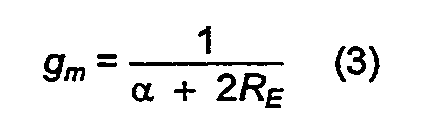
gain control amplifier 11, a post-amplifier 12, anAGC detecting circuit 13, and aDC amplifier 14. An input signal to the AGCAMP is input to the base of a transistor Q5 and is amplified by thegain control amplifier 11. The input signal is amplified by thepost-amplifier 12 and is subsequently input to theAGC detecting circuit 13 to be amplitude-detected. The AGC detection output is amplified by theDC amplifier 14 and is input to a differential electronic volume control constituted by transistors Q1 to Q4 to be subjected to AGC processing. A level at the start of AGC processing is set by theAGC detecting circuit 13. Assume that a gain of thegain control amplifier 11 is to be obtained. In this case, a mutual conductance gm of a differential circuit constituted by transistors Q5 and Q6 is represented by the following equation (vT is the thermal voltage of the transistors):
If a current I from a constant current source for the differential circuit is temperature-corrected by using a band gap regulator to establish


A substitution of equation (5) into equation (6) yields
Therefore, a collector voltage VC1 of the transistor Q1 is represented by equation (8):
An AC signal component vC1 of the collector voltage VC1 is represented by
That is, the input signal to thepost-amplifier 12 becomes the AC signal component vC1, and an output v₀ from the AGCAMP is given by the following equation, provided that the gain of thepost-amplifier 12 is represented by AP0:
If the AGCAMP is now performing an AGC operation, it can be assumed that an output from the AGCAMP is constant, and v₀ = V0C (11). At this time, the relationship between the input signal and the value ΔV given by
Equation (11) is solved with respect to ΔV as follows:
Equation (12) indicates the relationship between the input signal level vi and the difference in voltage between the transistors Q1 and Q2 in an AGCAMP operation. Referring to Fig. 2, the value ΔV corresponds to an AGC detection output obtained through theDC amplifier 14. In generally, the value ΔV is further amplified by an operational amplifier to obtain a level detection output. If the value ΔV is amplified by theoperational amplifier 15 in Fig. 2, a level detection output L₀ is given by
If equation (3) is substituted into equation (13), the level detection output L₀ is represented by
- In this conventional level detecting circuit, as indicated by equation (14):

since the level detection output L₀ includes the term of a thermal voltage, the value L₀ varies in relation to temperatures. For example, when a temperature t = -25°C, a level detection output L₁ is given by
When the temperature t = 75°C, a level detection output L₂ is given by
(where AP0, V₀, vi, and VB are constant with respect to temperatures.) A ratio of L₂ to L₁ is given by
- That is, the level detection output varies at 40% in the temperature range of -25°C to 75°C. The level detection output similarly varies with changes in the input signal vi. Since the level detection output always varies with signal changes from a low-level input to a high-level input, some kind of temperature correction is required in a level meter driving circuit to which the level detection output is input. Otherwise, the level meter varies with temperature changes.
- It is an object of the present invention to provide a level detecting circuit which can suppress variations in output level with changes in temperatures.
- It is another object of the present invention to provide a level detecting circuit which requires no temperature correction in a subsequent circuit to which a level detection output is input.
- In order to achieve the above objects, according to the present invention, there is provided a level detecting circuit comprising an operational amplifier for receiving differential outputs from an AGC detecting circuit as inverting and non-inverting inputs, a first resistor connected between one differential output of the AGC detecting circuit and the inverting input of the operational amplifier, a series circuit of second and third resistors inserted in a negative feedback loop between an output of the operational amplifier and the inverting input of the operational amplifier, a fourth resistor connected between the other differential output of the AGC detecting circuit and the non-inverting input of the operational amplifier, and a series circuit of fifth and sixth resistors connected between a bias voltage and the non-inverting input of the operational amplifier, wherein resistances of the first and fourth resistors and resistances of the second, third, fifth, and sixth are respectively set to be the same, and a temperature coefficient of each of the first, second, fourth, and fifth resistors and a temperature coefficient of each of the third and sixth resistors are set to have the same absolute value and opposite polarities.
-
- Fig. 1 is a block diagram showing an overall AGCAMP including an embodiment of the present invention;
- Fig. 2 is a block diagram showing an overall AGCAMP including a conventional level detecting circuit; and
- Fig. 3 is a block diagram showing an overall AGCAMP including another embodiment of the present invention.
- The present invention will be described below with reference to the accompanying drawings. Fig. 1 shows a level detecting circuit according to an embodiment of the present invention. Referring to Fig. 1, reference symbols R11, R12, R21, R22, R31, and R32 denote resistors.
Reference numeral 21 denotes an operational amplifier; 22, a post-amplifier; 23, an AGC detecting circuit; 24, a DC amplifier; and 28, a gain control amplifier. AGC detection outputs (from the DC amplifier) input toinput terminals operational amplifier 21, and a level detection output is output from anoutput terminal 10. An operation of this circuit will be described below. The resistors R11, R12, R21, and R22 have the same temperature coefficient. Each of the resistors R31 and R32 has a temperature coefficient having the same absolute value as that of the temperature coefficient of each of the resistors R11, R12, R21, and R22 but having a polarity opposite thereto. If the absolute value of the temperature coefficient of each of the resistors R11, R12, R21, R22, R31, and R32 is represented by α, resistors R1 (R11, R12), R2 (R21, R22), and R3 (R31, R32) can be expressed as follows:


- Assume that the values of the resistors R2 and R3 are the same at the temperature t = 0, and R₂₀ = R₃₀. In this case,

- A gain G₀ of the
operational amplifier 21 is then obtained as follows:
- According to equation (12), the AGC detection output ΔV obtained through the DC amplifier is given by

Therefore, the level detection output L₀₁ is obtained by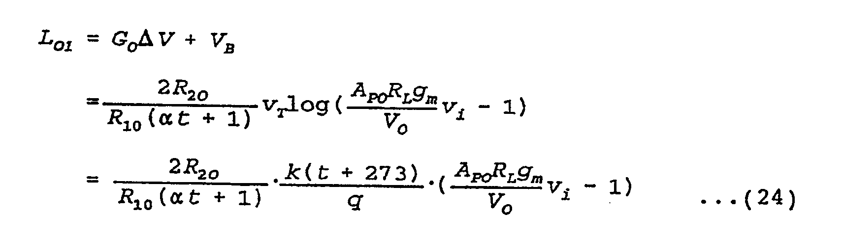
- As has been described above, according to the present invention, two resistors having the same resistance and the temperature coefficients with the same absolute value and opposite polarities are used as feedback resistors of the operational amplifier. Therefore, the level detection output L₀ is given by

If the temperature coefficient of each of the resistors R1 and R2 is +2500 ppm, and the temperature coefficient of the resistor R3 is -2500 ppm, since α is the absolute value of a temperature coefficient,

The value gm of equation (3) is substituted into equation (27) to obtain
At t = -25°C, the level detection output L₁ is given by
At t = 75°C, the level detection output L₂ is given by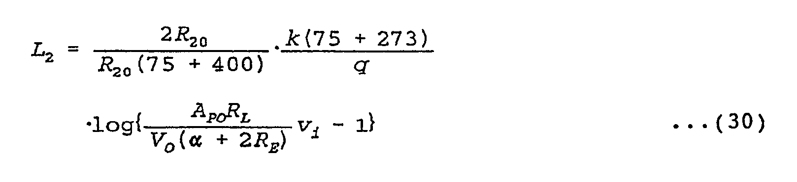
(Note that the values AP0 and vi do not vary with changes in temperature.)
A ratio of L₂ to L₁ is obtained as follows:
That is, the variations in level detection output can be suppressed to be 11% through the temperature range of -25°C to +75°C. In comparison with the conventional circuit, the variations in level detection output with changes in temperature are reduced by about 30%. - Fig. 3 shows a circuit according to the second embodiment of the present invention, which is a practical example of the
level detection circuit 21 in Fig. 1. Referring to Fig. 3, resistors R12,and R11 are respectively connected betweeninput terminals output terminal 10. - In this arrangement, the same effect as described above can be obtained with the resistors R11, R12, R21, R22, R31, and R32 having the same relationship as that of the resistors in Fig. 1.
Claims (3)
- A level detecting circuit characterized by comprising:
an operational amplifier (21) for receiving differential outputs from an AGC detecting circuit (23) as inverting and non-inverting inputs;
a first resistor (R11) connected between one differential output of said AGC detecting circuit (23) and the inverting input of said operational amplifier (21);
a series circuit of second and third resistors (R21, R31) inserted in a negative feedback loop between an output of said operational amplifier (21) and the inverting input of said operational amplifier (21);
a fourth resistor (R12) connected between the other differential output of said AGC detecting circuit (23) and the non-inverting input of said operational amplifier (21); and
a series circuit of fifth and sixth resistors (R22, R32) connected between a bias voltage and the non-inverting input of said operational amplifier (21),
wherein resistances of said first and fourth resistors (R21, R12) and resistances of said second, third, fifth, and sixth (R21, R31, R22, R32) are respectively set to be the same, and a temperature coefficient of each of said first, second, fourth, and fifth resistors (R11, R21, R12, R22) and a temperature coefficient of each of said third and sixth resistors (R31, R32) are set to have the same absolute value and opposite polarities. - A circuit according to claim 1, characterized in that said first and fourth resistors (R11, R12), said second and fifth resistors (R21, R22), and said third and sixth resistors (R31, R32) respectively have identical characteristics.
- A circuit for detecting a level of an input signal, comprising:
first and second terminals (8, 9) between which said input signal is supplied;
an operational amplifier (Q37 - Q41) having first and second input nodes and an output node;
a first resistor (R12) connected between said first terminal (8) and the first input node of said operational amplifier (Q37 - Q41);
a second resistor (R11) connected between said second terminal (9) and the second input node of said operational amplifier (Q37 - Q41);
third and fourth resistors (R21, R31) connected in series between the first input node and the output node of said operational amplifier (Q37 - Q41); and
fifth and sixth resistors (R22, R32) connected in series between the second input node of said operational amplifier (Q37 - Q41) and a bias potential point, temperature coefficients of said first to sixth (R12, R11, R21, R31, R22, R32) resistors being substantially equal to one another and a polarity of the temperature coefficient of said first, second, third, and fifth resistors (R12, R11, R21, R22) being opposite to a polarity of the temperature coefficient of said fourth and sixth resistors (R31, R32).
Applications Claiming Priority (2)
| Application Number | Priority Date | Filing Date | Title |
|---|---|---|---|
| JP2128057A JP2560888B2 (en) | 1990-05-17 | 1990-05-17 | Level detection circuit |
| JP128057/90 | 1990-05-17 |
Publications (3)
| Publication Number | Publication Date |
|---|---|
| EP0457582A2 true EP0457582A2 (en) | 1991-11-21 |
| EP0457582A3 EP0457582A3 (en) | 1992-06-17 |
| EP0457582B1 EP0457582B1 (en) | 1996-03-27 |
Family
ID=14975417
Family Applications (1)
| Application Number | Title | Priority Date | Filing Date |
|---|---|---|---|
| EP91304396A Expired - Lifetime EP0457582B1 (en) | 1990-05-17 | 1991-05-16 | Level detecting circuit |
Country Status (4)
| Country | Link |
|---|---|
| US (1) | US5404058A (en) |
| EP (1) | EP0457582B1 (en) |
| JP (1) | JP2560888B2 (en) |
| DE (1) | DE69118239T2 (en) |
Cited By (3)
| Publication number | Priority date | Publication date | Assignee | Title |
|---|---|---|---|---|
| AU635101B2 (en) * | 1989-12-22 | 1993-03-11 | Societe Anonyme Dite Alcatel Cit | A circuit for measuring the level of an electrical signal and including offset correction means, and application thereof to amplifiers having automatic gain control |
| EP0727669A3 (en) * | 1995-02-17 | 1997-06-11 | Landis & Gyr Tech Innovat | Temperature compensation means |
| CN114761814A (en) * | 2019-12-12 | 2022-07-15 | 罗伯特·博世有限公司 | Device for measuring a current through a choke and method for operating a device for measuring a current through a choke |
Families Citing this family (7)
| Publication number | Priority date | Publication date | Assignee | Title |
|---|---|---|---|---|
| KR100398167B1 (en) * | 1995-06-07 | 2003-12-31 | 가부시끼가이샤 히다치 세이사꾸쇼 | Portable satellite communication device |
| JP3479404B2 (en) * | 1996-03-29 | 2003-12-15 | アルプス電気株式会社 | Multi-stage variable gain amplifier circuit |
| US5912583A (en) * | 1997-01-02 | 1999-06-15 | Texas Instruments Incorporated | Continuous time filter with programmable bandwidth and tuning loop |
| DE19806394C1 (en) * | 1998-02-17 | 1999-08-26 | Bosch Gmbh Robert | Circuit for amplifying a difference voltage signal |
| US6259307B1 (en) * | 1998-10-14 | 2001-07-10 | Texas Instruments Incorporated | Temperature compensated voltage gain stage |
| US6140872A (en) * | 1999-10-28 | 2000-10-31 | Burr-Brown Corporation | Offset-compensated amplifier input stage and method |
| IL172797A (en) * | 2005-12-25 | 2012-09-24 | Elbit Systems Ltd | Real-time image scanning and processing |
Family Cites Families (12)
| Publication number | Priority date | Publication date | Assignee | Title |
|---|---|---|---|---|
| US3686517A (en) * | 1971-09-02 | 1972-08-22 | Gen Electric | Temperature compensation means for electronic circuit |
| US3808469A (en) * | 1972-10-27 | 1974-04-30 | Bell & Howell Co | Temperature compensation circuit for sensor of physical variables such as temperature and pressure |
| US3912997A (en) * | 1972-11-16 | 1975-10-14 | Systron Donner Corp | Bias and scale factor temperature compensation networks, for use in a force rebalance system |
| US3973147A (en) * | 1975-10-28 | 1976-08-03 | General Motors Corporation | Temperature measuring circuit |
| JPS52106054U (en) * | 1976-02-09 | 1977-08-12 | ||
| US4267468A (en) * | 1979-04-23 | 1981-05-12 | Motorola, Inc. | Temperature sensing circuit |
| JPS56118362A (en) * | 1980-02-22 | 1981-09-17 | Toshiba Corp | Semiconductor integrated circuit device |
| JPS5884722A (en) * | 1981-11-14 | 1983-05-20 | Matsushita Electric Works Ltd | Manufacturing method of patterned molding |
| JP2636829B2 (en) * | 1981-12-17 | 1997-07-30 | 富士通株式会社 | Differential circuit |
| US4611129A (en) * | 1983-04-22 | 1986-09-09 | Nec Corporation | Signal conversion circuit |
| FR2556464B1 (en) * | 1983-12-07 | 1986-09-19 | Renault | DEVICE FOR TEMPERATURE COMPENSATION OF A SENSOR AND ITS ADJUSTMENT METHOD |
| US4853646A (en) * | 1988-07-19 | 1989-08-01 | Fairchild Semiconductor Corporation | Temperature compensated bipolar circuits |
-
1990
- 1990-05-17 JP JP2128057A patent/JP2560888B2/en not_active Expired - Fee Related
-
1991
- 1991-05-16 EP EP91304396A patent/EP0457582B1/en not_active Expired - Lifetime
- 1991-05-16 DE DE69118239T patent/DE69118239T2/en not_active Expired - Fee Related
-
1994
- 1994-07-27 US US08/281,344 patent/US5404058A/en not_active Expired - Lifetime
Cited By (3)
| Publication number | Priority date | Publication date | Assignee | Title |
|---|---|---|---|---|
| AU635101B2 (en) * | 1989-12-22 | 1993-03-11 | Societe Anonyme Dite Alcatel Cit | A circuit for measuring the level of an electrical signal and including offset correction means, and application thereof to amplifiers having automatic gain control |
| EP0727669A3 (en) * | 1995-02-17 | 1997-06-11 | Landis & Gyr Tech Innovat | Temperature compensation means |
| CN114761814A (en) * | 2019-12-12 | 2022-07-15 | 罗伯特·博世有限公司 | Device for measuring a current through a choke and method for operating a device for measuring a current through a choke |
Also Published As
| Publication number | Publication date |
|---|---|
| JP2560888B2 (en) | 1996-12-04 |
| DE69118239D1 (en) | 1996-05-02 |
| EP0457582A3 (en) | 1992-06-17 |
| US5404058A (en) | 1995-04-04 |
| JPH0423507A (en) | 1992-01-27 |
| DE69118239T2 (en) | 1996-10-02 |
| EP0457582B1 (en) | 1996-03-27 |
Similar Documents
| Publication | Publication Date | Title |
|---|---|---|
| US4105942A (en) | Differential amplifier circuit having common mode compensation | |
| KR960705399A (en) | SIGNAL CONDITIONING APPARATUS AND METHOD EXHIBITING ACCURATE INPUT IMPEDANCE AND GAIN CHARACTERISTICS OVER COMMON MODE RANGE AND OPERATIONAL ENVIRONMENTS | |
| EP0457582B1 (en) | Level detecting circuit | |
| JPH06188657A (en) | Circuit for connecting exponential function step to automatic gain control circuit, automatic gain control circuit and temperature compensation circuit | |
| EP0196906A2 (en) | Automatic gain control detection circuit | |
| EP0563776A2 (en) | Signal detecting circuit apparatus | |
| US4528499A (en) | Modified bridge circuit for measurement purposes | |
| US4001602A (en) | Electronic analog divider | |
| US2820855A (en) | High impedance transistor amplifier | |
| JPH05145350A (en) | Amplifier circuit | |
| EP0478389A1 (en) | Amplifier having polygonal-line characteristics | |
| US4694248A (en) | Magnetic field sensor compensated for offset error | |
| US20190319595A1 (en) | Amplitude control with signal swapping | |
| EP0388890B1 (en) | Reactance control circuit with a DC amplifier for minimizing a variation of a reference reactance value | |
| CA1301862C (en) | Logarithmic amplification circuit for obtaining output voltage corresponding to difference between logarithmically amplified values of two input currents | |
| EP0903847A1 (en) | Amplifier circuit | |
| JPH0918745A (en) | Video signal clamp circuit | |
| US3405367A (en) | Quiescent current stabilized transistor amplifier | |
| US6114909A (en) | Differential amplifier for correcting offsets at inputs using low capacitance capacitor | |
| KR890007395Y1 (en) | Mid-band frequency amplifier circuit | |
| JPS6334360Y2 (en) | ||
| US3466560A (en) | Stable amplifier having a stable quiescent point | |
| JPS622706A (en) | Parallel feedback type amplifier circuit | |
| JPH08148954A (en) | Variable gain amplifier | |
| US5767741A (en) | Self compensating differential circuit |
Legal Events
| Date | Code | Title | Description |
|---|---|---|---|
| PUAI | Public reference made under article 153(3) epc to a published international application that has entered the european phase |
Free format text: ORIGINAL CODE: 0009012 |
|
| 17P | Request for examination filed |
Effective date: 19910603 |
|
| AK | Designated contracting states |
Kind code of ref document: A2 Designated state(s): DE FR GB |
|
| PUAL | Search report despatched |
Free format text: ORIGINAL CODE: 0009013 |
|
| AK | Designated contracting states |
Kind code of ref document: A3 Designated state(s): DE FR GB |
|
| 17Q | First examination report despatched |
Effective date: 19940526 |
|
| GRAH | Despatch of communication of intention to grant a patent |
Free format text: ORIGINAL CODE: EPIDOS IGRA |
|
| GRAA | (expected) grant |
Free format text: ORIGINAL CODE: 0009210 |
|
| AK | Designated contracting states |
Kind code of ref document: B1 Designated state(s): DE FR GB |
|
| REF | Corresponds to: |
Ref document number: 69118239 Country of ref document: DE Date of ref document: 19960502 |
|
| ET | Fr: translation filed | ||
| PLBE | No opposition filed within time limit |
Free format text: ORIGINAL CODE: 0009261 |
|
| STAA | Information on the status of an ep patent application or granted ep patent |
Free format text: STATUS: NO OPPOSITION FILED WITHIN TIME LIMIT |
|
| 26N | No opposition filed | ||
| REG | Reference to a national code |
Ref country code: GB Ref legal event code: IF02 |
|
| REG | Reference to a national code |
Ref country code: GB Ref legal event code: 732E |
|
| REG | Reference to a national code |
Ref country code: FR Ref legal event code: TP |
|
| PGFP | Annual fee paid to national office [announced via postgrant information from national office to epo] |
Ref country code: DE Payment date: 20080522 Year of fee payment: 18 |
|
| PGFP | Annual fee paid to national office [announced via postgrant information from national office to epo] |
Ref country code: GB Payment date: 20080521 Year of fee payment: 18 |
|
| GBPC | Gb: european patent ceased through non-payment of renewal fee |
Effective date: 20090516 |
|
| REG | Reference to a national code |
Ref country code: FR Ref legal event code: ST Effective date: 20100129 |
|
| PG25 | Lapsed in a contracting state [announced via postgrant information from national office to epo] |
Ref country code: FR Free format text: LAPSE BECAUSE OF NON-PAYMENT OF DUE FEES Effective date: 20090602 |
|
| PGFP | Annual fee paid to national office [announced via postgrant information from national office to epo] |
Ref country code: FR Payment date: 20080514 Year of fee payment: 18 |
|
| PG25 | Lapsed in a contracting state [announced via postgrant information from national office to epo] |
Ref country code: GB Free format text: LAPSE BECAUSE OF NON-PAYMENT OF DUE FEES Effective date: 20090516 |
|
| PG25 | Lapsed in a contracting state [announced via postgrant information from national office to epo] |
Ref country code: DE Free format text: LAPSE BECAUSE OF NON-PAYMENT OF DUE FEES Effective date: 20091201 |