EP0457595B1 - Appareil de communication pour transmettre et recevoir des signaux de communication sur une ligne commune de transmission - Google Patents
Appareil de communication pour transmettre et recevoir des signaux de communication sur une ligne commune de transmission Download PDFInfo
- Publication number
- EP0457595B1 EP0457595B1 EP91304422A EP91304422A EP0457595B1 EP 0457595 B1 EP0457595 B1 EP 0457595B1 EP 91304422 A EP91304422 A EP 91304422A EP 91304422 A EP91304422 A EP 91304422A EP 0457595 B1 EP0457595 B1 EP 0457595B1
- Authority
- EP
- European Patent Office
- Prior art keywords
- bus
- transmission line
- signal
- transmitting
- transmission
- Prior art date
- Legal status (The legal status is an assumption and is not a legal conclusion. Google has not performed a legal analysis and makes no representation as to the accuracy of the status listed.)
- Expired - Lifetime
Links
- 230000005540 biological transmission Effects 0.000 title claims description 115
- 238000004891 communication Methods 0.000 title claims description 55
- 230000000630 rising effect Effects 0.000 claims description 3
- 230000005855 radiation Effects 0.000 description 10
- 238000007493 shaping process Methods 0.000 description 10
- 238000010586 diagram Methods 0.000 description 6
- 239000003990 capacitor Substances 0.000 description 5
- 230000002411 adverse Effects 0.000 description 3
- 238000000034 method Methods 0.000 description 3
- 230000000694 effects Effects 0.000 description 2
- 230000010363 phase shift Effects 0.000 description 2
- 230000007704 transition Effects 0.000 description 2
- 238000013461 design Methods 0.000 description 1
- 230000008030 elimination Effects 0.000 description 1
- 238000003379 elimination reaction Methods 0.000 description 1
- 230000002452 interceptive effect Effects 0.000 description 1
- 238000011835 investigation Methods 0.000 description 1
- 230000002093 peripheral effect Effects 0.000 description 1
- 238000012545 processing Methods 0.000 description 1
- 230000005236 sound signal Effects 0.000 description 1
- 238000001228 spectrum Methods 0.000 description 1
Images



Classifications
-
- H—ELECTRICITY
- H04—ELECTRIC COMMUNICATION TECHNIQUE
- H04L—TRANSMISSION OF DIGITAL INFORMATION, e.g. TELEGRAPHIC COMMUNICATION
- H04L25/00—Baseband systems
- H04L25/02—Details ; arrangements for supplying electrical power along data transmission lines
- H04L25/0264—Arrangements for coupling to transmission lines
- H04L25/028—Arrangements specific to the transmitter end
- H04L25/0286—Provision of wave shaping within the driver
-
- H—ELECTRICITY
- H03—ELECTRONIC CIRCUITRY
- H03K—PULSE TECHNIQUE
- H03K17/00—Electronic switching or gating, i.e. not by contact-making and –breaking
- H03K17/51—Electronic switching or gating, i.e. not by contact-making and –breaking characterised by the components used
- H03K17/56—Electronic switching or gating, i.e. not by contact-making and –breaking characterised by the components used by the use, as active elements, of semiconductor devices
- H03K17/60—Electronic switching or gating, i.e. not by contact-making and –breaking characterised by the components used by the use, as active elements, of semiconductor devices the devices being bipolar transistors
- H03K17/66—Switching arrangements for passing the current in either direction at will; Switching arrangements for reversing the current at will
-
- H—ELECTRICITY
- H03—ELECTRONIC CIRCUITRY
- H03K—PULSE TECHNIQUE
- H03K4/00—Generating pulses having essentially a finite slope or stepped portions
- H03K4/94—Generating pulses having essentially a finite slope or stepped portions having trapezoidal shape
-
- H—ELECTRICITY
- H04—ELECTRIC COMMUNICATION TECHNIQUE
- H04L—TRANSMISSION OF DIGITAL INFORMATION, e.g. TELEGRAPHIC COMMUNICATION
- H04L25/00—Baseband systems
- H04L25/02—Details ; arrangements for supplying electrical power along data transmission lines
- H04L25/0264—Arrangements for coupling to transmission lines
- H04L25/0272—Arrangements for coupling to multiple lines, e.g. for differential transmission
- H04L25/0274—Arrangements for ensuring balanced coupling
-
- H—ELECTRICITY
- H04—ELECTRIC COMMUNICATION TECHNIQUE
- H04L—TRANSMISSION OF DIGITAL INFORMATION, e.g. TELEGRAPHIC COMMUNICATION
- H04L25/00—Baseband systems
- H04L25/02—Details ; arrangements for supplying electrical power along data transmission lines
- H04L25/0264—Arrangements for coupling to transmission lines
- H04L25/0292—Arrangements specific to the receiver end
Definitions
- the present invention relates to communication apparatus, more particularly to communication apparatus suitable for use in a multiplex transmission system in which a plurality of control circuits (hereinafter referred to as ECU) are capable of transmitting and receiving communication signals through a common transmission line.
- ECU control circuits
- a communication signal to be transmitted among ECUs has been expressed by combination of square wave signals and information transmitted by comparing a demodulated signal received by an ECU with a predetermined threshold value.
- harmonics of baseband are radiated and superposed on the radio frequency band, adversely affecting other devices, for example, by interfering with the reception of radio programs. It is therefore important to suppress the radiation of harmonics noise.
- One possibility is not to transmit the square wave as generated by a processing circuit but to transmit after modulation to a trapezoidal wave, the trapezoidal wave then being received by each ECU after demodulation to the square wave with reference to a constant threshold value preset in the receiving circuit.
- spectrum power of the harmonics is reduced by utilizing the trapezoidal wave for the communication signal and thereby radiation of noise is reduced to a very small amount.
- WO88/05979 discloses a device for the remote transmission of video signals. Video and audio signals on different lines are combined in an adder, which has two outputs. One output leads to a first current generator which feeds a first transmission line and the other output leads through an inverter to a second current generator which feeds a second transmission line. A receiving circuit is also provided for signals on the two transmission lines. The receiving circuit includes a differential amplifier and a de-modulator to check the signals.
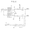
- a square wave signal received from an input terminal 1 from a transmitter Tx is branched to two routes, each of these square wave signals is respectively processed by trapezoidal wave shaping circuits T1, T2.
- One signal waveform is inverted and the pair of signals are transmitted to different transmission lines of the balanced two-wire system through output terminals 2, 3.
- These two signal waveforms are compared in amplitude by a comparator 30 in the receiving side and then demodulated into the square wave signals so as to suppress modulation and demodulation errors as much as possible.
- the circuit shown in Fig. 6 is certainly capable of reducing modulation and demodulation errors but also gives rise to adverse effects due to radiation of harmonics noise when used for communication at intermediate transmission rates of about 100 kbps.
- one output waveform is transmitted as the extremely accurate inverse (i.e has the opposite polarity) of the other output in such balanced two-wire transmission system, the radiation of harmonics noise can be suppressed even when the square wave signal is not modulated to the trapezoidal wave signal.
- One object of the present invention is to minimize modulation and demodulation errors without influence of fluctuation of GND potential difference between ECUs and power supply voltage difference and also favourably suppress influence of harmonics noise radiation even for intermediate and moreover high transmission rate signal.
- a first control circuit comprising at least a transmitting circuit and a second control circuit comprising at least a receiving circuit are connected by common transmission line means, wherein; the common transmission line means comprising a first and a second transmission line; the transmitting circuit comprising first transmitting means for converting information to be communicated into a communication signal for transmission along the first transmission line and second transmitting means for generating an inverted polarity communication signal for transmission along the second transmission line; and the receiving circuit comprising receiving means for comparing amplitudes of the communication signals transmitted from the transmitting circuit along the first and second transmission lines so as to demodulate the said information characterised in that the second transmitting means receives the communication signal from the first transmitting means to generate the inverted polarity communication signal.
- a first control circuit comprising at least a transmitting circuit and a second control circuit comprising at least a receiving circuit
- the common transmission line means comprising a first and a second transmission line
- the transmitting circuit comprising first transmitting means for converting an information carrying input signal, into a communication signal for transmission along the first transmission line and second transmitting means for generating an inverted polarity communication signal for transmission along the second transmission line
- the receiving circuit comprising receiving means for comparing amplitudes of the said communication signals transmitted from the transmitting circuit along the first and second transmission lines so as to demodulate the said information carried by the input signal, characterised in that the first transmitting means is for converting a square wave information carrying input signal at the rising and falling edges thereof into a communication signal having a predetermined gradient for transmission along the first transmission line and in that the second transmitting means receives the communication signal from the first transmitting means to generate the inverted polarity communications signal.
- Fig. 1 is a block diagram of a multiplex transmission system as a first embodiment of the present invention.
- ECU1 to ECU4 are mutually connected by two transmission lines BUS+ and BUS- of the parallel pair wires and each ECU comprises a CPU and a common transmitting and receiving circuit, M section.
- Tx means a CPU transmitting section; Rx, a CPU receiving section; TR, a transmitting circuit; RE, a receiving circuit.
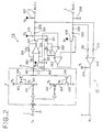
- Fig. 2 shows a embodied circuit structure of the transmitting and receiving circuit M of Fig. 1.
- the reference numeral 1 denotes an input terminal for inputting a square wave signal sent from the transmitting section Tx of CPU; 2, an output terminal for outputting an output signal shaped to a trapezoidal wave from the square wave signal to the transmission line BUS+; 3, an output terminal for outputting an output signal polarity inverted from the trapezoidal wave signal output from the output terminal 2 to the transmission line BUS-; 4, a receiving output terminal for inputting the signal demodulated to the square wave signal from the trapezoidal wave signal inputted from the transmission lines BUS+ and BUS- to the receiving section Rx of CPU.
- T means a trapezoidal wave shaping circuit for shaping the square wave signal sent from the transmitting section Tx into the trapezoidal wave.
- 101, 102 denote FETs for driving current Miller circuit; 103 to 106, transistors forming a current Miller circuit; 107, 108, transistors for driving transmission lines; 201, an operational amplifier for adjusting BUS+ output signal level; 202, an operational amplifier for polarity inversion; 203, an operational amplifier for feedback of signal; 204, a comparator as a receiver.
- 301, 302 denote resistors for determining a current of a current Miller circuit having a resistance value R1; 301, 302, resistors for adjusting BUS+ output signal amplitude level having resistance values R2, R3; 305, a resistor for adjusting BUS+ output signal DC offset level; 306, 309, resistors for protecting a transistor for driving transmission lines; 307, 308, resistors for biasing the transmission lines BUS+ and BUS-; 310, 311, resistors for inverting the BUS+ signal having a resistance value R4; 312, 313, resistors for protecting a receiver; 314, a resistor for pulling up comparator output; 315, a resistor for deciding the BUS+ signal level.
- 401s denote a capacitor for setting transmission time of the BUS+ signal having a capacitance value C; 402, a capacitor for noise elimination.
- 501 denotes a diode for protecting reverse surge and disabling operation of BUS- with the signal sent to BUS+ from the other ECU; 502, a diode for protecting reverse surge.
- a square wave signal conveying transmitting information from the transmitting section Tx of CPU is input to the input terminal 1.
- the signal to be applied to the gate of FET 101 becomes “L” level and FET 101 turns OFF because it is an N-channel type transistor. Therefore, a transistor 103 and a transistor 104 which forms a current Miller circuit together with the transistor 103 are turned OFF and thereby a current does not flow from the transistor 104.
- FET 102 is turned ON and a constant current determined by V1/R1 flows into a transistor 105 by means of the resistor 302.
- the similar constant current also flows into a collector of a transistor 106 forming a current Miller circuit together with the transistor 105.
- a capacitor 401 is charged, it is discharged due to a constant current flowing into the transistor 106 and the potential VA at the point A drops linearly to almost the GND potential.
- the trapezoidal wave shaping circuit T With operation of the trapezoidal wave shaping circuit T, the square wave signal inputted to the input terminal 1 is modulated to a trapezoidal wave signal and thereby a trapezoidal wave signal appears at the point A.
- This trapezoidal wave signal is applied to a negative (-) terminal of the operational amplifier 201.
- a base potential of the transistor 107 changes with the amplitude of (R3/R2)V1 in accordance with change of potential VA at the point A with reference to the preset potential VOS and this amplitude of base potential is lowered as much as the amplitude in comparison with that when the potential VA at the point A is equal to the GND potential while VA is V1.
- the capacitor 402 is provided for eliminating noise.
- An output of this operational amplifier 201 is then inputted to the base of the transistor 107.
- an emitter potential is higher as much as VBE than the base potential and is also lowered linearly following the base potential.
- an emitter potential is higher as much as VBE than the base potential and also increases linearly following the base potential.
- a signal having the potential which is set higher as much as a voltage drop caused by the diode 501 and resistor 306 from the emitter potential is transmitted to the transmission line BUS+ from the output terminal 2.
- an emitter potential of the transistor 107 is input to the negative (-) terminal of the operational amplifier 202 through a resistor 311.
- a potential VOS set by a resistor 305 is input to the positive (+) terminal of the operational amplifier 202, just like the positive (+) terminal of the operational amplifier 201.
- a resistance value of resistors 310, 311 is R4
- an output of the operational amplifier 202 is expressed by the following equation when an emitter potential of the transistor 107 is V.
- VOS - (VE - VOS) 2VOS - VE
- This output voltage is equal to an inverted value of the emitter potential VE with reference to the setting potential VOS.
- An output of this operational amplifier 202 is inputted to a base of the transistor 108 through an operational amplifier 203.
- an emitter potential VE of the transistor 107 when an emitter potential VE of the transistor 107 is lowered linearly, a base potential to be applied to the transistor 108 increases linearly and an emitter potential of the transistor 108 increases linearly following increase of a base potential and is kept at a potential which is lower as much as VBE than the base potential.
- a base potential to be applied to the base of the transistor 108 lowers linearly, and an emitter potential of the transistor 108 is lower as much as VBE than the base potential and lowers linearly following the base potential.
- the operational amplifier 203 structures a voltage follower and controls the base potential of the transistor 108 with an output potential of the operational amplifier 202 so that the inverted emitter potential of the transistor 107 becomes equal to the emitter potential of the transistor 108.
- the positive (+) terminal of a comparator 204 is connected to the transmission line BUS+ through a protection resistor 313, while the negative (-) terminal thereof to the transmission line BUS- through a protection resistor 312. Therefore, the comparator 204 defines "H" level as a result of comparison when a signal potential applied to the positive (+) terminal is higher than a signal potential applied to the negative (-) potential or "L" level when relationship of signal potential is reversed and outputs such signal levels from the receiving output terminal 4.
- a square wave signal is transmitted from Tx 1 of CPU 1, then modulated to a trapezoidal waveform by the TR section of the transmitting and receiving circuit M within ECU 1 and is transmitted to the transmission line BUS+.
- an inverted signal is then shaped from the signal waveform modulated to the trapezoidal waveform and is transmitted to another transmission line BUS-.
- Each output data is then inputted to ECU 2, it is demodulated to the square wave signal through comparison and decision in the RE section of the M section within ECU 2, then input to Rx 2 of CPU 2 and is then received by CPU 2.
- each ECU is capable, in Fig. 1, of executing mutual transmission or reception in accordance with the protocol (transmission regulation).
- the emitter potentials of the transistors 107, 108 are respectively inputted to the terminals of the operational amplifier 203 forming the emitter follower circuit, even when there is a difference in the base-emitter voltage VBE of the transistors 107, 108, an accurate polarity inverted waveforms can be output without any influence of such voltage difference.
- a diode 501 is inserted between the transmission line BUS+ and the transistor 107 so that an inverted signal is formed from the signal transmitted to the transmission line BUS+ from the other ECU, disabling operation of the other transmission line BUS-.
- the diode 501 also operates to protect the circuit from reverse surge voltage.
- the aforementioned first embodiment shapes the signal waveform polarity inverted through voltage feedback by the operational amplifier 203, while the second embodiment realizes current feedback.
- the receiving circuit (RE) is identical to the circuit shown in Fig. 2, only the transmitting circuit (TR) of M section is indicated in Fig. 3.
- the reference numeral 251 denotes an operational amplifier for amplifying BUS+ output signal voltage level (amplitude); 252, an operational amplifier for adjusting BUS+ output signal level; 253, 254, 256, 257, operational amplifiers for voltage follower; 255, an operational amplifier for differentially amplifying a voltage across a BUS+ monitor resistor 357; 258, an operational amplifier for differentially amplifying a voltage across a BUS- monitor resistor 357; 259, an operational amplifier for feedback.
- 353, 354 denote resistors for amplifying BUS+ output signal voltage level (amplitude) having resistance values R2, R3; 355, 356, resistors for adjusting BUS+ output signal level having resistance values R4, R5; 357, a resistor for BUS+ output current monitor having a resistance value R6; 358 to 361, resistors for differentially amplifying a voltage across the resistor 357 having the equal resistance value R7; 362 to 365, resistors for differentially amplifying a voltage across the resistor 366 having the equal resistance value R8; 366, a resistor for BUS- output current monitor having a resistance value R6; 367, 368, resistors for BUS- bias having the equal resistance value R9.
- the square wave signal inputted to the input terminal 1 is modulated to a corresponding trapezoidal wave signal by the trapezoidal waveform shaping circuit T just like the first embodiment and a trapezoidal wave signal appears at the point A. Therefore, a trapezoidal wave signal having the amplitude of almost V1 is inputted to the positive (+) terminal of the operational amplifier 251.
- a voltage to be applied to the base of the transistor 157 namely a base potential of the transistor 107 changes in the amplitude (R5/R4)V2 in accordance with change of the potential VA appearing at the point A around a potential V2/2 to be applied to the positive (+) terminal and therefore a voltage which is higher as much as VBE than the base potential appears at the emitter of the transistor 107.
- the operational amplifiers 253, 254 form a voltage follower so that a current which is equal to a drive current of the transistor 157 flows into the monitor resistor 357. Therefore, in Fig. 3, the right side potential of the resistors 358, 360 becomes equal to VE, VE + IE R6, respectively.
- This output potential becomes an input of the positive (+) terminal of the operational amplifier 259.
- a current flowing to the monitor resistor 366 is defined as IE′ and a number of ECUs to be connected is set to N
- an emitter potential VE′ of the transistor 108 is expressed as follows.
- VE′ IE′ (R6 + R9/N) + Vf Therefore, an anode potential of the diode 502 is expressed by VE′ - IE′ R6 and it is applied to the positive (+) terminal of the operational amplifier 256.
- a potential VE′ is applied to the positive (+) terminal of the operational amplifier 257.
- these operational amplifiers 256, 257 receive a voltage across the monitor resistor 366 with each voltage follower circuit so that a current which is equal to the drive current of the transistor 108 flows to the monitor resistor 366 just like the BUS+ side. For this reason, an output voltage of the monitor resistor 366 becomes equal to VE′ - IE′ R6 and an output potential of the operational amplifier 257 becomes equal to VE′.
- This output potential becomes an input to the negative (-) terminal of the operational amplifier 259.
- the operational amplifier 259 controls a base potential of the transistor 108 so that the output voltages of the operational amplifiers 255 and 258 become equal. Therefore, following relationships are established.
- the second embodiment utilizing current feed back method is capable of eliminating an influence of fluctuation, for example, GND fluctuation of the signal level, particularly of signal level of BUS- in the grounding side and therefore this embodiment is especially suitable as the apparatus to be mounted on a vehicle wherein GND level easily changes due to driving by an actuator.
- This third embodiment is also of the current feed back type, like the second embodiment explained above, wherein the direction of the currents flowing into the transmission lines BUS+, BUS- is reversed. Since the receiving circuit of this third embodiment is identical to that shown in Fig. 2, only the transmitting circuit (TR) of M section is indicated in Fig. 4.
- the same or equivalent elements as those shown in Fig. 2 and Fig. 3 are defined by the same reference numerals.
- the reference numeral 110 denotes a transistor for driving transmission lines; 111 to 115, transistors to form a current Miller circuit; 601, 602, constant current circuits for improving the response characteristic of the circuit; 370, 371, compensation resistors of a current Miller circuit.
- the square wave signal inputted to the input terminal 1 is modulated to a corresponding trapezoidal wave signal, like the case of the first embodiment, by the trapezoidal waveform shaping circuit T and this trapezoidal wave signal appears at the point A.
- This trapezoidal wave signal is then applied to the base of the transistor 110.
- a base potential of the transistor 110 is lowered linearly, an emitter potential is higher as much as VBE than the base potential and is also lowered following the base potential.
- the base potential increases, it is higher as much as VBE than the base potential and linearly increases following the emitter potential.
- a signal which is higher as much as a voltage drop by the diode 501 than this emitter potential is transmitted to the transmission line BUS+ from the output terminal 2.
- constant currents generated by the constant current circuits 601, 602 are set equal to each other and resistance values of resistors 370, 371 are also set equal to each other.
- the other ECUs have resistance value which is equal to the BUS+ bias resistance 307 and total of N units of ECU are connected.
- a constant current of the constant current circuits 601, 602 is defined as I0, a signal current of BUS+ as I1, a current flowing into the resistor 307 as I2, a current flowing into the diode 501 as I3, an emitter current of the transistor 110 as I4, a collector current of the transistor 112 as I5, a collector current of the transistor 115 as I6, a current flowing into the diode 502 as I7, a current flowing into the resistor 308 as I8 and a signal current of BUS- as I9, following relationships are obtained.
- ECU 1 comprises a transmitting circuit and a receiving circuit as the center station and the other ECUs 2 to 4 comprises only one of the receiving circuit and the transmitting circuit as the peripheral stations.
- any type of transmission system may be employed as long as it is the balanced two-wire system.
- a twisted-pair system can also be employed as well as the parallel pair-wire as indicated in the embodiments explained above.
- a square wave signal is modulated into a trapezoidal wave signal by a trapezoidal waveform shaping circuit T, but it is also allowed to apply the present invention to a system where a square wave signal is transmitted without being modulated into a trapezoidal wave signal.
Landscapes
- Engineering & Computer Science (AREA)
- Power Engineering (AREA)
- Computer Networks & Wireless Communication (AREA)
- Signal Processing (AREA)
- Dc Digital Transmission (AREA)
- Noise Elimination (AREA)
Claims (10)
- Appareil de communication dans lequel un premier circuit de commande comprenant au moins un circuit de transmission (TR) et un second circuit de commande comprenant au moins un circuit de réception (RE) sont reliés à l'aide d'un moyen de ligne de transmission commune,
le moyen de ligne de transmission commune comprenant une première et un seconde lignes de transmission (BUS+, BUS-),
le circuit de transmission (TR) comprenant un premier moyen d'émission pour convertir les informations à communiquer en un signal de communication pour une émission sur la première ligne de transmission (BUS+) et un second moyen d'émission pour générer un signal de communication de polarité inverse destiné à une émission sur la seconde ligne de transmission (BUS-), et
le circuit de réception (RE) comprenant un moyen de réception destiné à comparer les amplitudes des signaux de communication émis à partir du circuit de transmission sur les première et seconde lignes de transmission (BUS+, BUS-) de façon à démoduler ladite information, caractérisé en ce que le second moyen d'émission est agencé pour recevoir le signal de communication à partir du premier moyen d'émission pour générer le signal de communication de polarité inverse. - Appareil de communication selon la revendication 1, dans lequel le second moyen de transmission est agencé pour générer un signal de communication de polarité inverse par une contre-réaction en tension ou une contre-réaction en courant avec le signal de la première ligne de transmission.
- Appareil de communication dans lequel un premier circuit de commande comprenant au moins un circuit d'émission (TR) et un second circuit de commande comprenant au moins un circuit de réception (RE) sont reliés par un moyen de ligne de transmission commune (BUS+, BUS-),
le moyen de ligne de transmission commune comprenant une première et un seconde lignes de transmission (BUS+, BUS-),
le circuit de transmission (TR) comprenant un premier moyen de transmission destiné à convertir un signal d'entrée porteur d'informations en un signal de communication pour l'émission sur la première ligne de transmission (BUS+) et un second moyen de transmission destiné à générer un signal de communication de polarité inverse pour l'émission sur la seconde ligne de transmission (BUS-),
le circuit de réception (RE) comprenant un moyen de réception destiné à comparer l'amplitude desdits signaux de communication transmis à partir du circuit de transmission sur les première et seconde lignes de transmission (BUS+, BUS-) de façon à démoduler lesdites informations portées par le signal d'entrée, caractérisé en ce que le premier moyen d'émission est destiné à convertir un signal d'entrée porteur d'informations d'onde carrée, aux fronts montant et descendant de celui-ci, en un signal de communication présentant un gradient prédéterminé pour l'émission sur la première ligne de transmission (BUS+) et en ce que le second moyen d'émission est agencé pour recevoir le signal de communication à partir du premier moyen d'émission pour générer le signal de communication de polarité inverse. - Appareil de communication selon les revendications 1, 2 ou 3, dans lequel le second moyen d'émission comprend un moyen (202) destiné à entrer une tension de signal de communication émis à partir de la première ligne de transmission (BUS+) pour générer le signal de polarité inverse.
- Appareil de communication selon les revendications 1, 2 ou 3, dans lequel le second moyen d'émission comprend un moyen de commande en courant pour contrôler un courant de façon à ce qu'un courant circulant dans la première ligne de transmission (BUS+) avec l'émission du signal de communication dans la première ligne de transmission (BUS+) et un courant circulant dans la seconde ligne de transmission (BUS-) avec l'émission du signal de polarité inverse dans la seconde ligne de transmission (BUS-), deviennent égaux en amplitude mais sont de sens opposé l'un l'autre par rapport sens d'émission de signal vers les première et seconde lignes de transmission (BUS+, BUS-).
- Appareil de communication selon la revendication 5, dans lequel le moyen de commande de courant comprend un premier moyen de détection de courant destiné à détecter un courant circulant dans la première ligne de transmission (BUS+), un second moyen de détection de courant destiné à détecter un courant circulant dans la seconde ligne de transmission (BUS-) et un moyen de commande (107, 108 ; 601, 602) destiné à commander un courant circulant dans la seconde ligne de transmission (BUS-) de façon à ce que les courants détectés par les premier et second moyens de détection de courant soient égaux en amplitude mais soient de sens opposés l'un l'autre par rapport au sens d'émission de signal dans les première et seconde lignes de transmission (BUS+, BUS-).
- Appareil de communication selon la revendication 5, dans lequel le moyen de détection de courant comporte un moyen de commande destiné à extraire un courant circulant dans la première ligne de transmission (BUS+) par l'intermédiaire d'un circuit de courant de Miller (111 à 115) et contrôlant les courants circulant dans la seconde ligne de transmission sur la base du courant extrait, de façon à ce que ces courants deviennent égaux en amplitude mais de sens inverses l'un avec l'autre par rapport au sens d'émission du signal dans les première et seconde lignes de transmission (BUS+, BUS-).
- Appareil de communication selon les revendications 1, 2 ou 3, dans lequel le premier moyen d'émission comprend un moyen de validation de signal à sens unique de façon à valider l'émission du signal converti vers la première ligne de transmission (BUS+) en vue d'éviter au second moyen d'émission de fonctionner en état d'erreur avec l'entrée du signal provenant de la première ligne de transmission (BUS+).
- Appareil de communication selon les revendications 1, 2 ou 3, dans lequel les premier et second circuits de commande comprennent les moyens d'émission et de réception pour une émission et une réception mutuelles de signaux.
- Appareil de communication selon les revendications 1, 2 ou 3, dans lequel le premier circuit de commande comprend un moyen d'émission et un moyen de réception, le second circuit de commande ne comprend qu'un circuit de réception (RE) pour recevoir un signal de communication issu du premier circuit de commande, l'appareil comprenant en outre un troisième circuit de commande comportant un moyen pour transmettre le signal de communication au premier circuit de commande.
Applications Claiming Priority (6)
| Application Number | Priority Date | Filing Date | Title |
|---|---|---|---|
| JP127870/90 | 1990-05-17 | ||
| JP12787090 | 1990-05-17 | ||
| JP21104090 | 1990-08-08 | ||
| JP211040/90 | 1990-08-08 | ||
| JP90643/91 | 1991-04-22 | ||
| JP3090643A JPH0752870B2 (ja) | 1990-05-17 | 1991-04-22 | 通信装置 |
Publications (2)
| Publication Number | Publication Date |
|---|---|
| EP0457595A1 EP0457595A1 (fr) | 1991-11-21 |
| EP0457595B1 true EP0457595B1 (fr) | 1995-08-23 |
Family
ID=27306495
Family Applications (1)
| Application Number | Title | Priority Date | Filing Date |
|---|---|---|---|
| EP91304422A Expired - Lifetime EP0457595B1 (fr) | 1990-05-17 | 1991-05-16 | Appareil de communication pour transmettre et recevoir des signaux de communication sur une ligne commune de transmission |
Country Status (4)
| Country | Link |
|---|---|
| US (1) | US5355390A (fr) |
| EP (1) | EP0457595B1 (fr) |
| JP (1) | JPH0752870B2 (fr) |
| DE (1) | DE69112268T2 (fr) |
Families Citing this family (17)
| Publication number | Priority date | Publication date | Assignee | Title |
|---|---|---|---|---|
| JP3137809B2 (ja) * | 1993-07-20 | 2001-02-26 | 株式会社日立製作所 | 送受信回路 |
| US5535241A (en) * | 1994-05-31 | 1996-07-09 | Texas Instruments Incorporated | Signal transmission system and method of operation |
| FR2726708B1 (fr) * | 1994-11-09 | 1997-01-31 | Peugeot | Dispositif d'adaptation d'une interface de ligne d'une station raccordee a un reseau de transmission d'informations multiplexees |
| US5684831A (en) * | 1995-03-17 | 1997-11-04 | Delco Electronics Corp. | Data bus with noise immunity |
| US5629641A (en) * | 1996-02-06 | 1997-05-13 | Advanced Micro Devices, Inc. | Differential CMOS current amplifier with controlled bandwidth and common mode distortion |
| EP0822662A3 (fr) * | 1996-08-01 | 2001-03-21 | Siemens Aktiengesellschaft | Circuit d'interface |
| US6288592B1 (en) * | 1998-01-21 | 2001-09-11 | Gennum Corporation | Cable driver with controlled linear rise and fall |
| JP4158285B2 (ja) | 1998-08-28 | 2008-10-01 | 株式会社デンソー | 電気負荷の駆動装置 |
| EP1001535B1 (fr) * | 1998-11-10 | 2005-01-26 | STMicroelectronics S.r.l. | Circuit servant à commander le taux de variation de la tension de sortie d'un circuit d'attaque à configuration symétrique |
| US6771675B1 (en) * | 2000-08-17 | 2004-08-03 | International Business Machines Corporation | Method for facilitating simultaneous multi-directional transmission of multiple signals between multiple circuits using a single transmission line |
| EP1349491B1 (fr) | 2000-12-07 | 2013-04-17 | Children's Medical Center Corporation | Systeme de soins medicaux a interpretation automatisee |
| DE112006003744T5 (de) | 2006-02-17 | 2009-01-02 | Mitsubishi Electric Corp. | Einrichtung für ein Fahrzeug und ein Kommunikationsschnittstellen-Schaltkreis zur Verwendung in dieser Einrichtung |
| CN101499821B (zh) * | 2009-03-12 | 2013-01-30 | 苏州旭创科技有限公司 | 长距离40g qsfp通信有源铜缆组件的设计方法 |
| US9625838B2 (en) | 2014-11-28 | 2017-04-18 | Canon Kabushiki Kaisha | Electrophotographic apparatus, process cartridge, and image forming method |
| CN110297788B (zh) * | 2016-07-21 | 2024-03-01 | 华为技术有限公司 | 发送电路、接收电路和串行信号传输系统 |
| CN109408766B (zh) * | 2018-09-26 | 2023-05-16 | 国网山西省电力公司电力科学研究院 | 一种梯形图频率计算的方法 |
| CN112751589B (zh) * | 2020-12-31 | 2023-03-28 | 屈新苗 | 一种直流输电线路的斩波信号传输电路及传输方法 |
Family Cites Families (13)
| Publication number | Priority date | Publication date | Assignee | Title |
|---|---|---|---|---|
| DE125310C (fr) * | ||||
| US3711651A (en) * | 1970-12-30 | 1973-01-16 | R Connell | Polarity separation multiplex |
| US4054910A (en) * | 1976-02-26 | 1977-10-18 | Tel-E-Tel, Inc. | Communication system for the transmission of closed circuit television over an ordinary pair of wires |
| DD125310A1 (fr) * | 1976-04-19 | 1977-04-13 | ||
| NL191374C (nl) * | 1980-04-23 | 1995-06-16 | Philips Nv | Communicatiesysteem met een communicatiebus. |
| US4320521A (en) * | 1980-07-25 | 1982-03-16 | National Semiconductor Corporation | Data bus transceiver |
| CH657725A5 (de) * | 1981-04-14 | 1986-09-15 | Papst Motoren Kg | Anordnung zum unterdruecken von axialen rotorschwingungen bei einem elektrokleinmotor. |
| US4614882A (en) * | 1983-11-22 | 1986-09-30 | Digital Equipment Corporation | Bus transceiver including compensation circuit for variations in electrical characteristics of components |
| US4622482A (en) * | 1985-08-30 | 1986-11-11 | Motorola, Inc. | Slew rate limited driver circuit which minimizes crossover distortion |
| JPS62237895A (ja) * | 1986-04-09 | 1987-10-17 | Nippon Denso Co Ltd | 車載通信装置 |
| FR2610464A1 (fr) * | 1987-02-04 | 1988-08-05 | Cgv Comp Gen Videotech | Procede et dispositifs de transmission de signaux par conducteurs de petites sections |
| JPH07105819B2 (ja) * | 1987-07-08 | 1995-11-13 | ファナック株式会社 | デジタル差動信号伝送装置 |
| US4890010A (en) * | 1988-12-22 | 1989-12-26 | Ncr Corporation | Matched current source serial bus driver |
-
1991
- 1991-04-22 JP JP3090643A patent/JPH0752870B2/ja not_active Expired - Fee Related
- 1991-05-16 DE DE69112268T patent/DE69112268T2/de not_active Expired - Fee Related
- 1991-05-16 US US07/700,698 patent/US5355390A/en not_active Expired - Lifetime
- 1991-05-16 EP EP91304422A patent/EP0457595B1/fr not_active Expired - Lifetime
Also Published As
| Publication number | Publication date |
|---|---|
| DE69112268T2 (de) | 1996-05-02 |
| US5355390A (en) | 1994-10-11 |
| DE69112268D1 (de) | 1995-09-28 |
| EP0457595A1 (fr) | 1991-11-21 |
| JPH0752870B2 (ja) | 1995-06-05 |
| JPH04219035A (ja) | 1992-08-10 |
Similar Documents
| Publication | Publication Date | Title |
|---|---|---|
| EP0457595B1 (fr) | Appareil de communication pour transmettre et recevoir des signaux de communication sur une ligne commune de transmission | |
| US4493092A (en) | Interface circuit for digital signal transmission system | |
| US3993867A (en) | Digital single signal line full duplex method and apparatus | |
| US4007382A (en) | Bipolar signal processing circuit | |
| US20160099821A1 (en) | Power line carrier/communications with improved immunity for transients and electromagnetic interferences | |
| KR910001164B1 (ko) | 디지틀 데이터 해독장치 및 방법 | |
| US20110158258A1 (en) | Communication signal processing apparatus and communication apparatus | |
| US4341927A (en) | Data transmission apparatus | |
| US5050190A (en) | Signal detection circuit not affected by minute voltage fluctuations contained in input signal and operation method therefor | |
| JPH03296359A (ja) | Isdnインタフェース回路 | |
| EP3896862A1 (fr) | Système et procédé de communication sur une ligne de transmission unifilaire | |
| JPS61139138A (ja) | トランシーバ | |
| US6445239B1 (en) | Bus coupling with amplitude-controlled transmission circuit | |
| US11309738B2 (en) | Recovery of modulation amplitude in wireless charger tx demodulation | |
| US4689605A (en) | Powering device for transmitters and receivers of a signal transmission system | |
| US5365120A (en) | Data slicer with hold | |
| US5712475A (en) | Light receiving circuit with variable threshold circuit | |
| US20030017807A1 (en) | Apparatus and method for bias compensation in line circuits | |
| CN1032398C (zh) | 数据总线接口装置 | |
| KR100780942B1 (ko) | 신호 전송 장치 및 신호 전송 방법 | |
| US6760380B1 (en) | Data transmission apparatus and method | |
| US3962639A (en) | System for reducing radio communication frequency bandwidth and increasing number of channels available | |
| US5835535A (en) | Data bus interface apparatus which measures voltage potential on the uplink line of the data bus and removes an AC component | |
| US20260100866A1 (en) | Communication system | |
| US3075129A (en) | Coded signal receiving and shaping circuit |
Legal Events
| Date | Code | Title | Description |
|---|---|---|---|
| PUAI | Public reference made under article 153(3) epc to a published international application that has entered the european phase |
Free format text: ORIGINAL CODE: 0009012 |
|
| AK | Designated contracting states |
Kind code of ref document: A1 Designated state(s): DE FR GB |
|
| 17P | Request for examination filed |
Effective date: 19911012 |
|
| 17Q | First examination report despatched |
Effective date: 19940310 |
|
| GRAA | (expected) grant |
Free format text: ORIGINAL CODE: 0009210 |
|
| AK | Designated contracting states |
Kind code of ref document: B1 Designated state(s): DE FR GB |
|
| REF | Corresponds to: |
Ref document number: 69112268 Country of ref document: DE Date of ref document: 19950928 |
|
| ET | Fr: translation filed | ||
| PLBE | No opposition filed within time limit |
Free format text: ORIGINAL CODE: 0009261 |
|
| STAA | Information on the status of an ep patent application or granted ep patent |
Free format text: STATUS: NO OPPOSITION FILED WITHIN TIME LIMIT |
|
| 26N | No opposition filed | ||
| REG | Reference to a national code |
Ref country code: GB Ref legal event code: 746 Effective date: 19970116 |
|
| REG | Reference to a national code |
Ref country code: GB Ref legal event code: IF02 |
|
| PGFP | Annual fee paid to national office [announced via postgrant information from national office to epo] |
Ref country code: GB Payment date: 20050511 Year of fee payment: 15 Ref country code: FR Payment date: 20050511 Year of fee payment: 15 |
|
| PGFP | Annual fee paid to national office [announced via postgrant information from national office to epo] |
Ref country code: DE Payment date: 20050512 Year of fee payment: 15 |
|
| PG25 | Lapsed in a contracting state [announced via postgrant information from national office to epo] |
Ref country code: GB Free format text: LAPSE BECAUSE OF NON-PAYMENT OF DUE FEES Effective date: 20060516 |
|
| PG25 | Lapsed in a contracting state [announced via postgrant information from national office to epo] |
Ref country code: DE Free format text: LAPSE BECAUSE OF NON-PAYMENT OF DUE FEES Effective date: 20061201 |
|
| GBPC | Gb: european patent ceased through non-payment of renewal fee |
Effective date: 20060516 |
|
| REG | Reference to a national code |
Ref country code: FR Ref legal event code: ST Effective date: 20070131 |
|
| PG25 | Lapsed in a contracting state [announced via postgrant information from national office to epo] |
Ref country code: FR Free format text: LAPSE BECAUSE OF NON-PAYMENT OF DUE FEES Effective date: 20060531 |