EP0457596A2 - Process for fabricating a thin film transistor - Google Patents
Process for fabricating a thin film transistor Download PDFInfo
- Publication number
- EP0457596A2 EP0457596A2 EP91304428A EP91304428A EP0457596A2 EP 0457596 A2 EP0457596 A2 EP 0457596A2 EP 91304428 A EP91304428 A EP 91304428A EP 91304428 A EP91304428 A EP 91304428A EP 0457596 A2 EP0457596 A2 EP 0457596A2
- Authority
- EP
- European Patent Office
- Prior art keywords
- layer
- insulating layer
- island
- substrate
- sides
- Prior art date
- Legal status (The legal status is an assumption and is not a legal conclusion. Google has not performed a legal analysis and makes no representation as to the accuracy of the status listed.)
- Granted
Links
Images


Classifications
-
- H—ELECTRICITY
- H10—SEMICONDUCTOR DEVICES; ELECTRIC SOLID-STATE DEVICES NOT OTHERWISE PROVIDED FOR
- H10D—INORGANIC ELECTRIC SEMICONDUCTOR DEVICES
- H10D86/00—Integrated devices formed in or on insulating or conducting substrates, e.g. formed in silicon-on-insulator [SOI] substrates or on stainless steel or glass substrates
- H10D86/01—Manufacture or treatment
- H10D86/021—Manufacture or treatment of multiple TFTs
- H10D86/0231—Manufacture or treatment of multiple TFTs using masks, e.g. half-tone masks
-
- H—ELECTRICITY
- H10—SEMICONDUCTOR DEVICES; ELECTRIC SOLID-STATE DEVICES NOT OTHERWISE PROVIDED FOR
- H10D—INORGANIC ELECTRIC SEMICONDUCTOR DEVICES
- H10D30/00—Field-effect transistors [FET]
- H10D30/01—Manufacture or treatment
- H10D30/021—Manufacture or treatment of FETs having insulated gates [IGFET]
- H10D30/031—Manufacture or treatment of FETs having insulated gates [IGFET] of thin-film transistors [TFT]
- H10D30/0312—Manufacture or treatment of FETs having insulated gates [IGFET] of thin-film transistors [TFT] characterised by the gate electrodes
- H10D30/0314—Manufacture or treatment of FETs having insulated gates [IGFET] of thin-film transistors [TFT] characterised by the gate electrodes of lateral top-gate TFTs comprising only a single gate
-
- H—ELECTRICITY
- H10—SEMICONDUCTOR DEVICES; ELECTRIC SOLID-STATE DEVICES NOT OTHERWISE PROVIDED FOR
- H10D—INORGANIC ELECTRIC SEMICONDUCTOR DEVICES
- H10D30/00—Field-effect transistors [FET]
- H10D30/01—Manufacture or treatment
- H10D30/021—Manufacture or treatment of FETs having insulated gates [IGFET]
- H10D30/031—Manufacture or treatment of FETs having insulated gates [IGFET] of thin-film transistors [TFT]
- H10D30/0321—Manufacture or treatment of FETs having insulated gates [IGFET] of thin-film transistors [TFT] comprising silicon, e.g. amorphous silicon or polysilicon
-
- H—ELECTRICITY
- H10—SEMICONDUCTOR DEVICES; ELECTRIC SOLID-STATE DEVICES NOT OTHERWISE PROVIDED FOR
- H10D—INORGANIC ELECTRIC SEMICONDUCTOR DEVICES
- H10D86/00—Integrated devices formed in or on insulating or conducting substrates, e.g. formed in silicon-on-insulator [SOI] substrates or on stainless steel or glass substrates
- H10D86/40—Integrated devices formed in or on insulating or conducting substrates, e.g. formed in silicon-on-insulator [SOI] substrates or on stainless steel or glass substrates characterised by multiple TFTs
- H10D86/60—Integrated devices formed in or on insulating or conducting substrates, e.g. formed in silicon-on-insulator [SOI] substrates or on stainless steel or glass substrates characterised by multiple TFTs wherein the TFTs are in active matrices
-
- H—ELECTRICITY
- H10—SEMICONDUCTOR DEVICES; ELECTRIC SOLID-STATE DEVICES NOT OTHERWISE PROVIDED FOR
- H10P—GENERIC PROCESSES OR APPARATUS FOR THE MANUFACTURE OR TREATMENT OF DEVICES COVERED BY CLASS H10
- H10P50/00—Etching of wafers, substrates or parts of devices
- H10P50/20—Dry etching; Plasma etching; Reactive-ion etching
- H10P50/26—Dry etching; Plasma etching; Reactive-ion etching of conductive or resistive materials
- H10P50/264—Dry etching; Plasma etching; Reactive-ion etching of conductive or resistive materials by chemical means
- H10P50/266—Dry etching; Plasma etching; Reactive-ion etching of conductive or resistive materials by chemical means by vapour etching only
- H10P50/267—Dry etching; Plasma etching; Reactive-ion etching of conductive or resistive materials by chemical means by vapour etching only using plasmas
- H10P50/268—Dry etching; Plasma etching; Reactive-ion etching of conductive or resistive materials by chemical means by vapour etching only using plasmas of silicon-containing layers
Definitions
- the present invention relates to a process for fabricating thin film transistors, and is applicable ularly to a process for fabricating thin film transistors (hereinafter called "TFT") at a low temperature, the TFTs being adapted for use in display devices and image sensors.
- TFT thin film transistors
- TFTs used for driving liquid crystal display devices and image sensors are fabricated in the same manner as the IC fabricating process.
- the ICs must be processed at about 1,000°C so as to effect crystallization, formation of insulating layers and activation of impurities, which requires that the substrate on which IDs are formed must be selected from materials which can withstand high temperatures.
- the commonest material is quartz. Such a requirement makes it difficult to use a large substrate on which ICs are formed.
- amorphous or polycrystalline substance is used as a starting material which is crystallized by the solid phase growth or by laser annealing.
- a TFT is a MOS type transistor.
- the performances of transistors depend upon the interface condition of the gate insulating layer and the semiconductor layer. When transistors are processed at low temperatures, the gate insulating layers are also processed at equally low temperatures.
- Thin semiconductor layers are formed in a desired shape on a substrate, and subjected to surface treatment with the use of hydrofluoric acid, etc. Then, gate insulating layers are formed by sputtering or by a CVD method. These methods are not appropriate for reducing the interfacial level density for an unknown reason. The reason has been investigated. The investigation teaches that thin semiconductor layers should be followed by the formation of gate insulating layers without pause before the thin semiconductor layers are exposed to atmosphere.
- the formation of thin semiconductor layers must be followed by the overlaying of gate insulating layers.
- the layer to be overlaid is formed in a desired island-shaped pattern in which the sides of the semiconductor layer are exposed outside. If the gate electrode is formed under this condition, the exposed sides of the semiconductor layer and the gate electrode are likely to come into contact with each other, thereby increasing the current leak. In order to prevent this current leak, it is required to cover the exposed sides of the semiconductor layer with an insulating layer 8 as shown in Figure 9, prior to the formation of the gate electrode.
- the insulating layer 8 is made of SiO2, which is a material in common use for making gate insulating layers, the SiO2 of the gate insulating layer 3 is simultaneously etched. This simultaneous etching leaves the insulating layer 8 from shaping, and even if SiO2 and SiO2 have a large etching selective ratio, the simultaneous fabrication by etching is difficult.
- a PSG is known in the art which is fabricated by doping the SiO2 of an insulating layer with phosphorus. The larger the amount of the added phosphorus is, the larger the selective ratio becomes, but the phosphorus diffuses from the sides of the semiconductor layer 2, thereby changing the characteristics of the thin film transistor (TFT).
- the thin film transistors fabricating process of the present invention comprises the steps of forming a multi-layer body on a substrate, the multi-layer body including a semiconductor layer, a gate insulating layer and a lower thin layer, patterning the multi-layer body into islands, thereby removing the other portions of the multi-layer body, forming an insulating layer on the sides of the island-patterned multi-layered portion by etching at a selective ratio between the constituents of the insulating layer and the lower thin layer, forming an upper thin layer, and etching the upper and lower thin layers into upper and lower gate electrodes by use of one resist pattern.
- the formation of the multi-layer body is conducted in a vacuum or inert-gas filled space, thereby preventing the multi-layer body from being exposed to the atmosphere.
- the multi-layered portion is etched with a reactive ion-etchant so as to make the sides of the islands perpendicular to the substrate.
- the insulating layer on the sides of the islands is made of Si3N4.
- the gate electrode layer is made of metal.
- the process comprises the steps of preparing a substrate having a first insulating layer on a surface, forming a multi-layer body on the insulating layer of the substrate, the multi-layer body including a semiconductor layer, a gate insulating layer and a lower thin layer, patterning the multi-layer body into island, thereby removing the other portions of the multi-layer body than the island, forming a second insulating layer on the sides of the island, forming an upper thin layer, and etching the upper and lower thin layers into gate electrodes by use of the same resist pattern.
- the first and the second insulating layers of the substrate are made of different materials.
- the second insulating layer on both sides of the island is formed by overlaying it on the whole surface of the substrate, and removing other than a portion on both sides of the island by anisotropic etching.
- the anisotropic etching is a plasma etching
- the spectroscopic characteristics of the plasma applied to the second insulating layer are detected throughout the etching process so as to detect a change in the spectroscopic characteristics occuring when the first insulating layer is exposed, thereby controlling the period of time over which the plasma etching is applied to the second insulating layer.
- the invention described herein makes possible the objective of providing a TFT fabricating process which can form TFTs over a relatively wide range of a substrate easily with a high yield of manufacture.
- a glass substrate 1, after it is cleansed, is placed on a plasma CVD apparatus.
- the substrate 1 is heated to a temperature ranging from 400°C to 600°C, and a SiH4 gas is decomposed by heat and plasma, and deposited on the glass substrate 1 so as to form an amorphous Si layer to a thickness of about 1000 angstroms.
- the deposited amorphous Si layer is annealed in a vacuum or in an inert gas atmosphere at 600°C for about 50 hours so as to form a polycrystalline silicon layer 2.
- a SiO2 layer is formed to a thickness of about 1000 angstroms by sputtering so as to make it into a gate insulating layer 3.
- the glass substrate 1 is transported from the plasma CVD apparatus to the sputtering furnace by way of the annealing furnace in a confined chamber kept in a vacuum or filled with an inert gas, thereby ensuring that the substrate is kept free from exposure to the atmosphere.
- a polycrystalline silicon layer is formed to a thickness of about 1000 angstroms by a vacuum CVD apparatus, so as to make a lower gate electrode 4a.
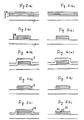
- the resulting three-layered structure is shown in Figures 2 (a) and 2 (b).
- the next step is shown in Figures 3 (a) and 3 (b), by which the three-layered layer is etched into an island-shaped pattern by use of a resist pattern produced in the transistor portion.
- the etching is a reactive ion-etching, which is called an anisotropic etching in which the sides of the island-patterned multi-layer portion are vertical to the surface of the substrate surface.
- the etchant can be a gaseous mixture of SF6 and CCl4 for a polycrystalline silicon layer, and a CHF3 gas for a SiO2 layer.
- a polycrystalline silicon layer is deposited by a vacuum CVD method to a thickness of about 2000 angstroms as an upper gate electrode 4b, and then the upper gate electrode 4b and a lower gate electrode 4a are formed by a reactive ion etchant through a resist pattern formed as a gate electrode.
- the finished gate electrode 4 is shown in Figure 1.
- any suitable impurities are ion injected on the substrate 1, and an activating annealling is carried out.
- the upper gate electrode 4a, the lower gate electrode 4b and the polycrystalline silicon layer which is later made into a source and a drain at opposite sides of the gate electrode, are made so as to have a low resistance with electrically conductivity.
- the next step is the stage shown in Figures 7 (a) and 7 (b) in which an insulating layer 6 is formed. More specifically, a SiO2 or a PSG layer having a phosphorus doping is formed on the whole surface of the substrate 1 by a normal pressure CVD method, and contact holes (not numbered) are formed in the layer 6 at the junction of electrodes. Other contact holes are formed in the layer 6 on a gate electrode 4 connected to an Al wiring, which is described in the next paragraph.
- Al layer 7 having a thickness of about 5000 angstroms is first formed by sputtering, and then it is made into Al layer wirings 7a and 7b of a predetermined shape by photo-etching as shown in Figures 8 (a) and 8 (b). In this way, the final TFT having a desired wiring as shown in Figure 1 is obtained.
- the insulating layer on the sides of the island that is, the island-patterned multi-layer portion, and the gate electrodes are made of different materials, thereby avoiding the difficulty resulting from the use of the same kind of material which is adopted under the known fabricating process.
- the insulating layer on the sides of the island-patterned multi-layer portion can be made of Si3N4 or other material if they do not unfavorably affect the semiconductor.
- the gate electrode can be made of metal such as Ti or W, instead of polycrystalline silicon, or made of a combination of them with silicide.
- a SiN film 22 is formed on the substrate 1 to a thickness of about 3000 angstroms by a plasma CVD apparatus after the substrate 1 is cleansed. Then an amorphous Si layer is formed on the first Si layer at a temperature of 400°C to 600°C by using a SiH4 diluted with H2 and decomposed by heat and plasma. This layer is about 1000 angstroms thick.
- the Si layer is annealed at 600°C at a vacuum or in an inert gas atmosphere for about 50 hours so as to make it into polycrystalline Si layer 23.
- a SiO2 is then formed by sputtering to a thickness of about 1000 angstroms from which a gate insulating layer is formed at a later stage. These processes are conducted without being exposed to atmosphere as described above.
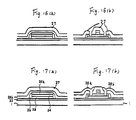
- Figure 11 shows the formation of a polycrystalline silicon layer having a thickness of about 1000 angstroms from which a first gate electrode 25a is formed.
- a first gate electrode 25a is formed.
- three layers 22, 23, and 25a are obtained, all of which are patterned by use of the same resist pattern into an island-shaped portion, hereinafter referred to the island as shown in Figure 12.
- a reactive ion etchant is used and an anisotropic etching is adopted so that after etching each vertical section is perpendicular to the substrate 1.
- a gaseous mixture of SF6 and CCl4 is used for the polycrystalline silicon layer and a CHF3 gas is used for the SiO2.
- the whole surface of the substrate 1 is covered with a SiO2 26 having a thickness of about 5000 angstroms by a sputtering device or a normal pressure CVD device.
- a reactive ion etchant is used to perform an anisotropic etching so as to remove the SiO2 26 until the only sides of the island remain as shown in Figure 14.
- Figure 18 shows the variations with time in the emitting light intensity from the initiation of the etching, of the spectrums of 388 nm of CN resulting from the etching gas CHF3 and the SiN layer 22 selected from the plasma emitting spectrums.
- the etching process is stopped. This ensures that a constant size of the SiO2 layer is formed on the sides of the island.
- the next step is to form a polycrystalline silicon layer having a thickness of about 2000 angstroms by a reduced pressure CVD device from which a second gate electrode 25b is made.
- a resist pattern is formed so as to shape the gate electrode as desired.
- the first gate electrode 25a and the second gate electrode 25b are etched with a reactive ion etchant at the same time.
- ion is injected into the gate electrodes 25a and 25b so as to effect an activated annealing, so that the polycrystalline silicon layer of the two gate electrodes and a polycrystalline silicon layer from which a drain is later formed are treated so as to have low resistance.
- a PSG layer is formed by doping the substrate 1 with SiO2 or phosphorus, and contact holes are made at desired spots so as to form an inter-layer insulating layer 7.
- the gate insulating layer is also provided with holes so that the source and drain and an Al electrode referred to below may be electrically connected.
- the contact hole is made in a layer 27 on the gate electrode 25 connected to an Al wiring referred to below (not shown).
- the next step is to form an Al layer to a thickness of about 5000 angstroms by sputtering to a desired shape for a source electrode 28a and a drain electrode 28b, which, as a thin film transistor and a circumferential wirings, is shown in Figure 17.
- the final TFT is shown in Figure 10.
- the material for the first insulating layer on the substrate 1 and the material for the second insulating layer on the sides of the island are replaceable, and any other materials can be used for the insulating layers on condition that they have different spectroscopic characteristics.
- the gate electrode can be made of metals such as Ti or W instead of the polycrystalline silicon.
Landscapes
- Thin Film Transistor (AREA)
Abstract
Description
- The present invention relates to a process for fabricating thin film transistors, and is applicable ularly to a process for fabricating thin film transistors (hereinafter called "TFT") at a low temperature, the TFTs being adapted for use in display devices and image sensors.
- TFTs used for driving liquid crystal display devices and image sensors are fabricated in the same manner as the IC fabricating process. The ICs must be processed at about 1,000°C so as to effect crystallization, formation of insulating layers and activation of impurities, which requires that the substrate on which IDs are formed must be selected from materials which can withstand high temperatures. The commonest material is quartz. Such a requirement makes it difficult to use a large substrate on which ICs are formed. In order to solve the problems arising at high temperatures, amorphous or polycrystalline substance is used as a starting material which is crystallized by the solid phase growth or by laser annealing.
- A TFT is a MOS type transistor. The performances of transistors depend upon the interface condition of the gate insulating layer and the semiconductor layer. When transistors are processed at low temperatures, the gate insulating layers are also processed at equally low temperatures.
- Thin semiconductor layers are formed in a desired shape on a substrate, and subjected to surface treatment with the use of hydrofluoric acid, etc. Then, gate insulating layers are formed by sputtering or by a CVD method. These methods are not appropriate for reducing the interfacial level density for an unknown reason. The reason has been investigated. The investigation teaches that thin semiconductor layers should be followed by the formation of gate insulating layers without pause before the thin semiconductor layers are exposed to atmosphere.
- In order to improve the performance of TFTs formed at low temperatures, it is necessary to reduce the interfacial level density between the semiconductor and gate insulating layers. In order to achieve this, the formation of thin semiconductor layers must be followed by the overlaying of gate insulating layers. To make the overlying layers as a TFT, the layer to be overlaid is formed in a desired island-shaped pattern in which the sides of the semiconductor layer are exposed outside. If the gate electrode is formed under this condition, the exposed sides of the semiconductor layer and the gate electrode are likely to come into contact with each other, thereby increasing the current leak. In order to prevent this current leak, it is required to cover the exposed sides of the semiconductor layer with an
insulating layer 8 as shown in Figure 9, prior to the formation of the gate electrode. In Figure 9, aninsulating substrate 1 on which asemiconductor layer 2, agate insulating layer 3, and a gate electrode 4 overlap one above another. If theinsulating layer 8 is made of SiO₂, which is a material in common use for making gate insulating layers, the SiO₂ of thegate insulating layer 3 is simultaneously etched. This simultaneous etching leaves theinsulating layer 8 from shaping, and even if SiO₂ and SiO₂ have a large etching selective ratio, the simultaneous fabrication by etching is difficult. A PSG is known in the art which is fabricated by doping the SiO₂ of an insulating layer with phosphorus. The larger the amount of the added phosphorus is, the larger the selective ratio becomes, but the phosphorus diffuses from the sides of thesemiconductor layer 2, thereby changing the characteristics of the thin film transistor (TFT). - The thin film transistors fabricating process of the present invention, which overcomes the above-discussed and numerous other disadvantages of the prior art, comprises the steps of forming a multi-layer body on a substrate, the multi-layer body including a semiconductor layer, a gate insulating layer and a lower thin layer, patterning the multi-layer body into islands, thereby removing the other portions of the multi-layer body, forming an insulating layer on the sides of the island-patterned multi-layered portion by etching at a selective ratio between the constituents of the insulating layer and the lower thin layer, forming an upper thin layer, and etching the upper and lower thin layers into upper and lower gate electrodes by use of one resist pattern.
- In a preferred embodiment, the formation of the multi-layer body is conducted in a vacuum or inert-gas filled space, thereby preventing the multi-layer body from being exposed to the atmosphere.
- In a preferred embodiment, the multi-layered portion is etched with a reactive ion-etchant so as to make the sides of the islands perpendicular to the substrate.
- In a preferred embodiment, the insulating layer on the sides of the islands is made of Si₃N₄.
- In a preferred embodiment, the gate electrode layer is made of metal.
- Alternatively, the process comprises the steps of preparing a substrate having a first insulating layer on a surface, forming a multi-layer body on the insulating layer of the substrate, the multi-layer body including a semiconductor layer, a gate insulating layer and a lower thin layer, patterning the multi-layer body into island, thereby removing the other portions of the multi-layer body than the island, forming a second insulating layer on the sides of the island, forming an upper thin layer, and etching the upper and lower thin layers into gate electrodes by use of the same resist pattern.
- In a preferred embodiment, the first and the second insulating layers of the substrate are made of different materials.
- In a preferred embodiment, the second insulating layer on both sides of the island is formed by overlaying it on the whole surface of the substrate, and removing other than a portion on both sides of the island by anisotropic etching.
- In a preferred embodiment, the anisotropic etching is a plasma etching, and the spectroscopic characteristics of the plasma applied to the second insulating layer are detected throughout the etching process so as to detect a change in the spectroscopic characteristics occuring when the first insulating layer is exposed, thereby controlling the period of time over which the plasma etching is applied to the second insulating layer.
- Thus, the invention described herein makes possible the objective of providing a TFT fabricating process which can form TFTs over a relatively wide range of a substrate easily with a high yield of manufacture.
- This invention is further described, by way of example, with reference to the accompanying drawings, in which:
- Figure 1 is a plan view showing a thin film transistor to be fabricated by the present invention;
- Figures 2 to 8 are diagrammatic sectional views, taken on lines A-A′ and B-B′ of Fig.1, showing the steps of fabricating a thin film transistor;
- Figure 9 is a sectional view showing a known thin film transistor;
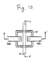
- Figure 10 is a plan view showing a thin film transistor according to a second example of the present invention;
- Figures 11 to 17 are diagrammatic sectional views, taken on lines A-A′ and B-B′ of Fig.10, showing the steps of performing the second example; and
- Figure 18 is a graph showing the intensities of an emitting light varying with time.
- Referring to Figures 1 to 8, a first example of the present invention will be described:
- As shown in Figures 2 (a) and 2 (b), a
glass substrate 1, after it is cleansed, is placed on a plasma CVD apparatus. Thesubstrate 1 is heated to a temperature ranging from 400°C to 600°C, and a SiH₄ gas is decomposed by heat and plasma, and deposited on theglass substrate 1 so as to form an amorphous Si layer to a thickness of about 1000 angstroms. The deposited amorphous Si layer is annealed in a vacuum or in an inert gas atmosphere at 600°C for about 50 hours so as to form apolycrystalline silicon layer 2. Then, a SiO₂ layer is formed to a thickness of about 1000 angstroms by sputtering so as to make it into agate insulating layer 3. In the course of conducting the steps described above, theglass substrate 1 is transported from the plasma CVD apparatus to the sputtering furnace by way of the annealing furnace in a confined chamber kept in a vacuum or filled with an inert gas, thereby ensuring that the substrate is kept free from exposure to the atmosphere. - Then, a polycrystalline silicon layer is formed to a thickness of about 1000 angstroms by a vacuum CVD apparatus, so as to make a lower gate electrode 4a. The resulting three-layered structure is shown in Figures 2 (a) and 2 (b).
- The next step is shown in Figures 3 (a) and 3 (b), by which the three-layered layer is etched into an island-shaped pattern by use of a resist pattern produced in the transistor portion. The etching is a reactive ion-etching, which is called an anisotropic etching in which the sides of the island-patterned multi-layer portion are vertical to the surface of the substrate surface. The etchant can be a gaseous mixture of SF₆ and CCl₄ for a polycrystalline silicon layer, and a CHF₃ gas for a SiO₂ layer.
- The steps advance to that shown in Figures 4 (a) and 4 (b), in which the whole surface of the
substrate 1 is covered with aSiO₂ layer 5 formed to a thickness of about 5000 angstroms by sputtering or a normal-pressure CVD method. Then, an anisotropic etching is carried out with a reactive ion etchant so that the SiO₂ remains only on the sides of the island-patterned multi-layer portion as shown in Figures 5 (a) and 5 (b). - Then, as shown in Figure 6 (a), a polycrystalline silicon layer is deposited by a vacuum CVD method to a thickness of about 2000 angstroms as an upper gate electrode 4b, and then the upper gate electrode 4b and a lower gate electrode 4a are formed by a reactive ion etchant through a resist pattern formed as a gate electrode. The finished gate electrode 4 is shown in Figure 1. Then, any suitable impurities are ion injected on the
substrate 1, and an activating annealling is carried out. In this way the upper gate electrode 4a, the lower gate electrode 4b and the polycrystalline silicon layer, which is later made into a source and a drain at opposite sides of the gate electrode, are made so as to have a low resistance with electrically conductivity. - The next step is the stage shown in Figures 7 (a) and 7 (b) in which an
insulating layer 6 is formed. More specifically, a SiO₂ or a PSG layer having a phosphorus doping is formed on the whole surface of thesubstrate 1 by a normal pressure CVD method, and contact holes (not numbered) are formed in thelayer 6 at the junction of electrodes. Other contact holes are formed in thelayer 6 on a gate electrode 4 connected to an Al wiring, which is described in the next paragraph. - An
Al layer 7 having a thickness of about 5000 angstroms is first formed by sputtering, and then it is made intoAl layer wirings - As is evident from the foregoing description, the insulating layer on the sides of the island, that is, the island-patterned multi-layer portion, and the gate electrodes are made of different materials, thereby avoiding the difficulty resulting from the use of the same kind of material which is adopted under the known fabricating process.
- The insulating layer on the sides of the island-patterned multi-layer portion can be made of Si₃N₄ or other material if they do not unfavorably affect the semiconductor. The gate electrode can be made of metal such as Ti or W, instead of polycrystalline silicon, or made of a combination of them with silicide.
- Referring to Figures 10 to 18, a second example will be described:
- A
SiN film 22 is formed on thesubstrate 1 to a thickness of about 3000 angstroms by a plasma CVD apparatus after thesubstrate 1 is cleansed. Then an amorphous Si layer is formed on the first Si layer at a temperature of 400°C to 600°C by using a SiH₄ diluted with H₂ and decomposed by heat and plasma. This layer is about 1000 angstroms thick. The Si layer is annealed at 600°C at a vacuum or in an inert gas atmosphere for about 50 hours so as to make it intopolycrystalline Si layer 23. A SiO₂ is then formed by sputtering to a thickness of about 1000 angstroms from which a gate insulating layer is formed at a later stage. These processes are conducted without being exposed to atmosphere as described above. - Figure 11 shows the formation of a polycrystalline silicon layer having a thickness of about 1000 angstroms from which a
first gate electrode 25a is formed. In this way threelayers substrate 1. As an etching gas, a gaseous mixture of SF₆ and CCl₄ is used for the polycrystalline silicon layer and a CHF₃ gas is used for the SiO₂. - Then, as shown in Figure 13, the whole surface of the
substrate 1 is covered with aSiO₂ 26 having a thickness of about 5000 angstroms by a sputtering device or a normal pressure CVD device. Afterward, a reactive ion etchant is used to perform an anisotropic etching so as to remove theSiO₂ 26 until the only sides of the island remain as shown in Figure 14. Figure 18 shows the variations with time in the emitting light intensity from the initiation of the etching, of the spectrums of 388 nm of CN resulting from the etching gas CHF₃ and theSiN layer 22 selected from the plasma emitting spectrums. When a critical level is ascertained where the emitting light intensity does not increase any longer, the etching process is stopped. This ensures that a constant size of the SiO₂ layer is formed on the sides of the island. - The next step is to form a polycrystalline silicon layer having a thickness of about 2000 angstroms by a reduced pressure CVD device from which a
second gate electrode 25b is made. As shown in Figure 15, a resist pattern is formed so as to shape the gate electrode as desired. With the use of the pattern, thefirst gate electrode 25a and thesecond gate electrode 25b are etched with a reactive ion etchant at the same time. - Then, ion is injected into the
gate electrodes - Then, a PSG layer is formed by doping the
substrate 1 with SiO₂ or phosphorus, and contact holes are made at desired spots so as to form an inter-layerinsulating layer 7. The gate insulating layer is also provided with holes so that the source and drain and an Al electrode referred to below may be electrically connected. The contact hole is made in alayer 27 on the gate electrode 25 connected to an Al wiring referred to below (not shown). - The next step is to form an Al layer to a thickness of about 5000 angstroms by sputtering to a desired shape for a source electrode 28a and a
drain electrode 28b, which, as a thin film transistor and a circumferential wirings, is shown in Figure 17. The final TFT is shown in Figure 10. - The material for the first insulating layer on the
substrate 1 and the material for the second insulating layer on the sides of the island are replaceable, and any other materials can be used for the insulating layers on condition that they have different spectroscopic characteristics. As described with respect to the first example, the gate electrode can be made of metals such as Ti or W instead of the polycrystalline silicon. - It is understood that various other modifications will be apparent to and can be readily made by those skilled in the art without departing from the scope and spirit of this invention. Accordingly, it is not intended that the scope of the claims appended hereto be limited to the description as set forth herein, but rather that the claims be construed as encompassing all the features of patentable novelty that reside in the present invention, including all features that would be treated as equivalents thereof by those skilled in the art to which this invention pertains.
Claims (10)
- A process for fabricating a thin film transistor, wherein a multi-layer body is formed on a substrate, the multi-layer body including a semiconductor layer, a gate insulating layer and a lower thin layer, and the multi-layer body is patterned into islands, thereby removing the other portions of the multi-layer body, characterised in that an insulating layer is formed on the sides of the island-patterned multi-layered portion by etching at a selective ratio between the constituents of the insulating layer and the lower thin layer, and in that an upper thin layer, and the upper and lower thin layers are etched into upper and lower gate electrodes by use of one resist pattern.
- A process as claimed in claim 1, wherein the formation of the multi-layer body is conducted in a vacuum or inert-gas filled space, thereby preventing the multi-layer body from being exposed to the atmosphere.
- A process as claimed in claim 1 or 2, wherein the multi-layered portion is etched with a reactive ion-etchant so as to make the sides of the island perpendicular to the substrate.
- A process as claimed in claim 1, 2 or 3, wherein the gate electrode layer is made of metal.
- A process for fabricating a thin film transistor, wherein a substrate is prepared so as to have a first insulating layer on a surface, a multilayer body is formed on the insulating layer of the substrate, the multi-layer body including a semiconductor layer, a gate insulating layer and a lower thin layer, and the multi-layer body is patterned into islands, thereby removing the other portions of the multi-layer body than the island, and wherein a second insulating layer is formed on the sides of the island, an upper thin layer is formed and the upper and lower thin layers are etched into gate electrodes by use of the same resist pattern.
- A process as claimed in claim 5, wherein the formation of the multi-layer body is conducted in a vacuum or inert-gas filled space, thereby preventing the multi-layer body from being exposed to the atmosphere.
- A process as claimed in claim 5 or 6, wherein the first and the second insulating layers of the substrate are made of different materials.
- A process as claimed in any of claims 5 to 7, wherein the second insulating layer on both sides of the island is formed by overlaying it on the whole surface of the substrate, and removing other than a portion on both sides of the island by anisotropic etching.
- A process as claimed in claim 8, wherein the anisotropic etching is a plasma etching, and wherein the spectroscopic characteristics of the plasma applied to the second insulating layer is detected throughout the etching process so as to detect a change in the spectroscopic characteristics occurring when the first insulating layer is exposed, thereby controlling the period of time over which the plasma etching is applied to the second insulating layer.
- A process as claimed in any preceding claim, wherein the insulating layer on the sides of the island is made of Si₃N₄.
Applications Claiming Priority (2)
| Application Number | Priority Date | Filing Date | Title |
|---|---|---|---|
| JP129973/90 | 1990-05-17 | ||
| JP12997390 | 1990-05-17 |
Publications (3)
| Publication Number | Publication Date |
|---|---|
| EP0457596A2 true EP0457596A2 (en) | 1991-11-21 |
| EP0457596A3 EP0457596A3 (en) | 1992-05-20 |
| EP0457596B1 EP0457596B1 (en) | 1995-12-06 |
Family
ID=15023018
Family Applications (1)
| Application Number | Title | Priority Date | Filing Date |
|---|---|---|---|
| EP91304428A Expired - Lifetime EP0457596B1 (en) | 1990-05-17 | 1991-05-16 | Process for fabricating a thin film transistor |
Country Status (3)
| Country | Link |
|---|---|
| US (1) | US5120667A (en) |
| EP (1) | EP0457596B1 (en) |
| DE (1) | DE69115118T2 (en) |
Cited By (3)
| Publication number | Priority date | Publication date | Assignee | Title |
|---|---|---|---|---|
| FR2728390A1 (en) * | 1994-12-19 | 1996-06-21 | Korea Electronics Telecomm | METHOD FOR FORMING A THIN FILM TRANSISTOR |
| US5681761A (en) * | 1995-12-28 | 1997-10-28 | Philips Electronics North America Corporation | Microwave power SOI-MOSFET with high conductivity metal gate |
| US8120111B2 (en) | 2003-04-11 | 2012-02-21 | Semiconductor Energy Laboratory Co., Ltd. | Thin film transistor including insulating film and island-shaped semiconductor film |
Families Citing this family (14)
| Publication number | Priority date | Publication date | Assignee | Title |
|---|---|---|---|---|
| US5753542A (en) * | 1985-08-02 | 1998-05-19 | Semiconductor Energy Laboratory Co., Ltd. | Method for crystallizing semiconductor material without exposing it to air |
| JP2508851B2 (en) * | 1989-08-23 | 1996-06-19 | 日本電気株式会社 | Active matrix substrate for liquid crystal display device and manufacturing method thereof |
| US5409851A (en) * | 1992-05-04 | 1995-04-25 | Goldstar Co., Ltd. | Method of making a thin film transistor |
| KR940010384A (en) * | 1992-10-23 | 1994-05-26 | 이헌조 | Method of manufacturing thin film transistor |
| JPH0766420A (en) * | 1993-08-31 | 1995-03-10 | Matsushita Electric Ind Co Ltd | Thin film processing method |
| KR0124958B1 (en) * | 1993-11-29 | 1997-12-11 | 김광호 | Thin film transistor for crystal liquid & manufacturing method of the same |
| JP3464285B2 (en) * | 1994-08-26 | 2003-11-05 | 株式会社半導体エネルギー研究所 | Method for manufacturing semiconductor device |
| JP3497627B2 (en) * | 1994-12-08 | 2004-02-16 | 株式会社東芝 | Semiconductor device and manufacturing method thereof |
| US6337229B1 (en) * | 1994-12-16 | 2002-01-08 | Semiconductor Energy Laboratory Co., Ltd. | Method of making crystal silicon semiconductor and thin film transistor |
| US6746905B1 (en) * | 1996-06-20 | 2004-06-08 | Kabushiki Kaisha Toshiba | Thin film transistor and manufacturing process therefor |
| KR100349366B1 (en) * | 1999-06-28 | 2002-08-21 | 주식회사 하이닉스반도체 | SOI device and method of manufacturing the same |
| JP4243455B2 (en) * | 2002-05-21 | 2009-03-25 | 日本電気株式会社 | Thin film transistor manufacturing method |
| US6963083B2 (en) * | 2003-06-30 | 2005-11-08 | Lg.Philips Lcd Co., Ltd. | Liquid crystal display device having polycrystalline TFT and fabricating method thereof |
| KR101860859B1 (en) * | 2011-06-13 | 2018-05-25 | 삼성디스플레이 주식회사 | Manufacturing method of thin film transistor, the thin film transistor manufactured by the same, manufacturing method of organic light emitting apparatus and the organic light emitting apparatus manufactured by the same |
Family Cites Families (10)
| Publication number | Priority date | Publication date | Assignee | Title |
|---|---|---|---|---|
| JPS5317069A (en) * | 1976-07-30 | 1978-02-16 | Fujitsu Ltd | Semiconductor device and its production |
| JPS56116627A (en) * | 1980-02-20 | 1981-09-12 | Chiyou Lsi Gijutsu Kenkyu Kumiai | Thin film semiconductor device |
| JPS58102560A (en) * | 1981-12-14 | 1983-06-18 | Fujitsu Ltd | Manufacture of thin film transistor |
| FR2566583B1 (en) * | 1984-06-22 | 1986-09-19 | Thomson Csf | METHOD FOR MANUFACTURING AT LEAST ONE THIN FILM FIELD-EFFECT TRANSISTOR, AND TRANSISTOR OBTAINED BY THIS METHOD |
| JPH0622245B2 (en) * | 1986-05-02 | 1994-03-23 | 富士ゼロックス株式会社 | Method of manufacturing thin film transistor |
| US4753896A (en) * | 1986-11-21 | 1988-06-28 | Texas Instruments Incorporated | Sidewall channel stop process |
| JPS63308386A (en) * | 1987-01-30 | 1988-12-15 | Sony Corp | Semiconductor device and manufacture thereof |
| JPH0687503B2 (en) * | 1987-03-11 | 1994-11-02 | 株式会社日立製作所 | Thin film semiconductor device |
| JPH0220820A (en) * | 1988-07-08 | 1990-01-24 | Minolta Camera Co Ltd | Image forming device |
| FR2651068B1 (en) * | 1989-08-16 | 1994-06-10 | France Etat | PROCESS FOR PRODUCING SILICON-ON-INSULATOR MOS MESA TRANSISTOR |
-
1991
- 1991-05-16 DE DE69115118T patent/DE69115118T2/en not_active Expired - Fee Related
- 1991-05-16 EP EP91304428A patent/EP0457596B1/en not_active Expired - Lifetime
- 1991-10-18 US US07/778,750 patent/US5120667A/en not_active Expired - Lifetime
Cited By (4)
| Publication number | Priority date | Publication date | Assignee | Title |
|---|---|---|---|---|
| FR2728390A1 (en) * | 1994-12-19 | 1996-06-21 | Korea Electronics Telecomm | METHOD FOR FORMING A THIN FILM TRANSISTOR |
| US5681761A (en) * | 1995-12-28 | 1997-10-28 | Philips Electronics North America Corporation | Microwave power SOI-MOSFET with high conductivity metal gate |
| US8120111B2 (en) | 2003-04-11 | 2012-02-21 | Semiconductor Energy Laboratory Co., Ltd. | Thin film transistor including insulating film and island-shaped semiconductor film |
| US9362307B2 (en) | 2003-04-11 | 2016-06-07 | Semiconductor Energy Laboratory Co., Ltd. | Thin film transistor, electronic device having the same, and method for manufacturing the same |
Also Published As
| Publication number | Publication date |
|---|---|
| US5120667A (en) | 1992-06-09 |
| EP0457596B1 (en) | 1995-12-06 |
| EP0457596A3 (en) | 1992-05-20 |
| DE69115118T2 (en) | 1996-05-30 |
| DE69115118D1 (en) | 1996-01-18 |
Similar Documents
| Publication | Publication Date | Title |
|---|---|---|
| US5120667A (en) | Process for fabricating a thin film transistor | |
| KR100372841B1 (en) | Method for fabricating semiconductor device with high quality crystalline silicon film | |
| US5766977A (en) | Method for producing semiconductor device | |
| CN100481512C (en) | Semiconductor device and method of fabricating the same | |
| JPH10135137A (en) | Crystalline semiconductor fabrication method | |
| JPH05109737A (en) | Method of manufacturing thin film transistor | |
| KR100607768B1 (en) | Thin film transistor and method for manufacturing same | |
| US20050082537A1 (en) | Semiconductor device and method for manufacturing the same | |
| US7160768B2 (en) | Method of manufacturing electronic device and method of manufacturing semiconductor device | |
| JPH04275436A (en) | Soimos transistor | |
| JPH0685258A (en) | Thin-film transistor and its manufacture | |
| JP2698724B2 (en) | Thin film transistor and method of manufacturing the same | |
| JP4901020B2 (en) | Method for manufacturing polysilicon thin film transistor | |
| US20050157222A1 (en) | Method of manufacturing semiconductor device | |
| JPH04226080A (en) | Manufacture of thin film transistor | |
| JPH0555578A (en) | Manufacture of thin film transistor | |
| JPH09213793A (en) | Semiconductor integrated circuit device and method of manufacturing the same | |
| JPH0666312B2 (en) | Method for manufacturing semiconductor device | |
| JP2513664B2 (en) | Method for manufacturing thin film transistor | |
| JPH07122752A (en) | Method of manufacturing thin film transistor | |
| JP3310567B2 (en) | Method for manufacturing semiconductor device | |
| JP2004165286A (en) | Method for manufacturing thin film transistor | |
| JPH09331067A (en) | Method for manufacturing semiconductor device | |
| JPS583252A (en) | Semiconductor integrated circuit device | |
| JPH0917798A (en) | Semiconductor device and manufacturing method thereof |
Legal Events
| Date | Code | Title | Description |
|---|---|---|---|
| PUAI | Public reference made under article 153(3) epc to a published international application that has entered the european phase |
Free format text: ORIGINAL CODE: 0009012 |
|
| 17P | Request for examination filed |
Effective date: 19910527 |
|
| AK | Designated contracting states |
Kind code of ref document: A2 Designated state(s): DE FR GB |
|
| PUAL | Search report despatched |
Free format text: ORIGINAL CODE: 0009013 |
|
| AK | Designated contracting states |
Kind code of ref document: A3 Designated state(s): DE FR GB |
|
| 17Q | First examination report despatched |
Effective date: 19940412 |
|
| GRAA | (expected) grant |
Free format text: ORIGINAL CODE: 0009210 |
|
| AK | Designated contracting states |
Kind code of ref document: B1 Designated state(s): DE FR GB |
|
| REF | Corresponds to: |
Ref document number: 69115118 Country of ref document: DE Date of ref document: 19960118 |
|
| ET | Fr: translation filed | ||
| PLBE | No opposition filed within time limit |
Free format text: ORIGINAL CODE: 0009261 |
|
| STAA | Information on the status of an ep patent application or granted ep patent |
Free format text: STATUS: NO OPPOSITION FILED WITHIN TIME LIMIT |
|
| 26N | No opposition filed | ||
| PGFP | Annual fee paid to national office [announced via postgrant information from national office to epo] |
Ref country code: DE Payment date: 20010508 Year of fee payment: 11 |
|
| PGFP | Annual fee paid to national office [announced via postgrant information from national office to epo] |
Ref country code: GB Payment date: 20010516 Year of fee payment: 11 |
|
| PGFP | Annual fee paid to national office [announced via postgrant information from national office to epo] |
Ref country code: FR Payment date: 20010518 Year of fee payment: 11 |
|
| REG | Reference to a national code |
Ref country code: GB Ref legal event code: IF02 |
|
| PG25 | Lapsed in a contracting state [announced via postgrant information from national office to epo] |
Ref country code: GB Free format text: LAPSE BECAUSE OF NON-PAYMENT OF DUE FEES Effective date: 20020516 |
|
| PG25 | Lapsed in a contracting state [announced via postgrant information from national office to epo] |
Ref country code: DE Free format text: LAPSE BECAUSE OF NON-PAYMENT OF DUE FEES Effective date: 20021203 |
|
| GBPC | Gb: european patent ceased through non-payment of renewal fee |
Effective date: 20020516 |
|
| PG25 | Lapsed in a contracting state [announced via postgrant information from national office to epo] |
Ref country code: FR Free format text: LAPSE BECAUSE OF NON-PAYMENT OF DUE FEES Effective date: 20030131 |
|
| REG | Reference to a national code |
Ref country code: FR Ref legal event code: ST |