EP0457638A1 - Verfahren zur Regelung der Helligkeit von Bildschirmen - Google Patents
Verfahren zur Regelung der Helligkeit von Bildschirmen Download PDFInfo
- Publication number
- EP0457638A1 EP0457638A1 EP91401146A EP91401146A EP0457638A1 EP 0457638 A1 EP0457638 A1 EP 0457638A1 EP 91401146 A EP91401146 A EP 91401146A EP 91401146 A EP91401146 A EP 91401146A EP 0457638 A1 EP0457638 A1 EP 0457638A1
- Authority
- EP
- European Patent Office
- Prior art keywords
- selective
- semi
- line
- addressing
- command
- Prior art date
- Legal status (The legal status is an assumption and is not a legal conclusion. Google has not performed a legal analysis and makes no representation as to the accuracy of the status listed.)
- Granted
Links
- 238000000034 method Methods 0.000 title claims abstract description 29
- 238000012423 maintenance Methods 0.000 claims description 45
- 239000004973 liquid crystal related substance Substances 0.000 claims description 11
- 239000011159 matrix material Substances 0.000 claims description 3
- 238000012217 deletion Methods 0.000 claims description 2
- 230000037430 deletion Effects 0.000 claims description 2
- 230000000007 visual effect Effects 0.000 abstract 1
- 210000004027 cell Anatomy 0.000 description 39
- 230000006870 function Effects 0.000 description 9
- PEDCQBHIVMGVHV-UHFFFAOYSA-N Glycerine Chemical compound OCC(O)CO PEDCQBHIVMGVHV-UHFFFAOYSA-N 0.000 description 4
- 210000002858 crystal cell Anatomy 0.000 description 3
- 230000005540 biological transmission Effects 0.000 description 2
- 239000003990 capacitor Substances 0.000 description 2
- 125000004122 cyclic group Chemical group 0.000 description 2
- 238000010586 diagram Methods 0.000 description 2
- 230000005684 electric field Effects 0.000 description 2
- 230000012447 hatching Effects 0.000 description 2
- 230000003446 memory effect Effects 0.000 description 2
- 241001080024 Telles Species 0.000 description 1
- 230000008901 benefit Effects 0.000 description 1
- 230000008859 change Effects 0.000 description 1
- 238000007796 conventional method Methods 0.000 description 1
- 238000012986 modification Methods 0.000 description 1
- 230000004048 modification Effects 0.000 description 1
- 230000008569 process Effects 0.000 description 1
- 238000012552 review Methods 0.000 description 1
- 230000000630 rising effect Effects 0.000 description 1
- 238000001228 spectrum Methods 0.000 description 1
- 239000010409 thin film Substances 0.000 description 1
Images

Classifications
-
- G—PHYSICS
- G09—EDUCATION; CRYPTOGRAPHY; DISPLAY; ADVERTISING; SEALS
- G09G—ARRANGEMENTS OR CIRCUITS FOR CONTROL OF INDICATING DEVICES USING STATIC MEANS TO PRESENT VARIABLE INFORMATION
- G09G3/00—Control arrangements or circuits, of interest only in connection with visual indicators other than cathode-ray tubes
- G09G3/20—Control arrangements or circuits, of interest only in connection with visual indicators other than cathode-ray tubes for presentation of an assembly of a number of characters, e.g. a page, by composing the assembly by combination of individual elements arranged in a matrix no fixed position being assigned to or needed to be assigned to the individual characters or partial characters
- G09G3/2007—Display of intermediate tones
- G09G3/2014—Display of intermediate tones by modulation of the duration of a single pulse during which the logic level remains constant
-
- G—PHYSICS
- G09—EDUCATION; CRYPTOGRAPHY; DISPLAY; ADVERTISING; SEALS
- G09G—ARRANGEMENTS OR CIRCUITS FOR CONTROL OF INDICATING DEVICES USING STATIC MEANS TO PRESENT VARIABLE INFORMATION
- G09G3/00—Control arrangements or circuits, of interest only in connection with visual indicators other than cathode-ray tubes
- G09G3/20—Control arrangements or circuits, of interest only in connection with visual indicators other than cathode-ray tubes for presentation of an assembly of a number of characters, e.g. a page, by composing the assembly by combination of individual elements arranged in a matrix no fixed position being assigned to or needed to be assigned to the individual characters or partial characters
- G09G3/22—Control arrangements or circuits, of interest only in connection with visual indicators other than cathode-ray tubes for presentation of an assembly of a number of characters, e.g. a page, by composing the assembly by combination of individual elements arranged in a matrix no fixed position being assigned to or needed to be assigned to the individual characters or partial characters using controlled light sources
- G09G3/28—Control arrangements or circuits, of interest only in connection with visual indicators other than cathode-ray tubes for presentation of an assembly of a number of characters, e.g. a page, by composing the assembly by combination of individual elements arranged in a matrix no fixed position being assigned to or needed to be assigned to the individual characters or partial characters using controlled light sources using luminous gas-discharge panels, e.g. plasma panels
- G09G3/288—Control arrangements or circuits, of interest only in connection with visual indicators other than cathode-ray tubes for presentation of an assembly of a number of characters, e.g. a page, by composing the assembly by combination of individual elements arranged in a matrix no fixed position being assigned to or needed to be assigned to the individual characters or partial characters using controlled light sources using luminous gas-discharge panels, e.g. plasma panels using AC panels
- G09G3/298—Control arrangements or circuits, of interest only in connection with visual indicators other than cathode-ray tubes for presentation of an assembly of a number of characters, e.g. a page, by composing the assembly by combination of individual elements arranged in a matrix no fixed position being assigned to or needed to be assigned to the individual characters or partial characters using controlled light sources using luminous gas-discharge panels, e.g. plasma panels using AC panels using surface discharge panels
-
- G—PHYSICS
- G09—EDUCATION; CRYPTOGRAPHY; DISPLAY; ADVERTISING; SEALS
- G09G—ARRANGEMENTS OR CIRCUITS FOR CONTROL OF INDICATING DEVICES USING STATIC MEANS TO PRESENT VARIABLE INFORMATION
- G09G2320/00—Control of display operating conditions
- G09G2320/06—Adjustment of display parameters
- G09G2320/0626—Adjustment of display parameters for control of overall brightness
Definitions
- the invention relates to a method for controlling display screens, making it possible to increase the dynamic range for adjusting the brightness of these screens.
- the invention applies to screens of the internal memory type.
- screens with internal memory we mean screens whose cells which form the elementary image seals keep the "registered" state in which they are likely to be activated, after the end of the state control signal " inscribed ", as is the case in particular for plasma panels and particularly those of the alternative type.
- the lighting conditions around the screen can vary by a factor of around 1,000 (from a few tens of lux indoors, with dimmed lighting, to a few tens of thousands of lux in an outdoor environment, in full sun) .
- the conventional method for adjusting the luminance of the screen consists in adjusting the frequency of signals. called maintenance signals, by which cells in the so-called “on” or “registered” state produce light.
- plasma panels of the alternative type which have a memory effect
- these panels are for example of the type with two crossed electrodes to define a discharge cell as described in a French patent in the name of THOMSON-CSF published with the number 2.417.848; these panels can also be of the coplanar maintenance type, in which for the same cell, addressing discharges and maintenance discharges are carried out between different electrodes, as described in particular in a European patent application EP-A-0135382 .
- These panels include a plurality of cells generally arranged in rows and columns.
- the addressing of a given cell is carried out by the selection of two crossed electrodes to which one applies, at a given time, appropriate voltages so that the potential difference causes between these electrodes a writing discharge or an erasing discharge .
- a classic addressing method consists in operating line by line: in this case all the cells of a given line are controlled simultaneously (semi-selective operation), to be “registered” or “erased”, erased for example and this operation is followed by a selective operation during which one or more selected cells of this same line are "registered".
- the semi-selective operation followed by the selective operation is performed for each line, with an offset of time from one line to another which corresponds to the duration of a line cycle.
- the addressing phase is followed by a maintenance phase during which the cells in the "registered" state are activated, that is to say produce light.
- maintenance signals are applied simultaneously to all the cells, and cause maintenance discharges which provide most of the light emission perceived by an observer.
- the maintenance signal is an alternating signal made up of successive voltage slots with opposite polarities: each change of sign of the alternating signal (rising or falling edges) generates a discharge in the gas and an emission of light at the level of the or affected cells.
- each change of sign of the alternating signal (rising or falling edges) generates a discharge in the gas and an emission of light at the level of the or affected cells.
- the basic slots for both registration and erasure have substantially the same amplitude as the maintenance signals, and consequently they can also generate comparable discharges. at maintenance landfills, with light emission. Consequently, it can be considered that the addressing phases contain at least one maintenance cycle.
- the frequency of the maintenance signal can be made adjustable and by adjusting it, the overall luminance of the screen is adjusted.
- the refresh rates of the information that is to say of the renewal of the image, as well as physical limitations on the durations of the discharges, greatly limit the possibilities of adjusting the luminance of the screen. using the frequency variation of the maintenance signal.
- the time of a cycle of line CL corresponds to:
- maintenance cycles is equal to:
- FIGs 1a and 1b to be read together are diagrams which show the distribution over time of these different phases, for only two consecutive lines Li and Li + 1.
- the addressing phase PA1 is followed by a maintenance phase PE1 which ends at an instant t3 when a second addressing phase PA2 begins. From time t0, the first addressing phase PA1 and the following maintenance phase PE define a first line cycle CL1 which ends at time t3 where a second line cycle TL2 begins, and thus up to a CLn cycle; all these line cycles CL1, CL2, CLn being constructed in the same way.
- the addressing of the cells of the line Li is carried out in the first cycle of line CL1 (during the first phase of addressing PA1)
- the addressing of the line Li + 1 is carried out during the second phase of addressing PA2 of the second line cycle CL2.
- the addressing which follows for the line Li is then carried out 480 line cycles after the first cycle CL1, during the cycle CLn for example.
- FIGS. 1a, 1b the fact that the addressing was carried out during a given addressing period is symbolized by hatching in the slots which represent the addressing phases PA1, PA2, ... PAn.
- this addressing phase can be followed by a phase of maintenance PE1, PE2, PEn whose duration is equal to a maximum of 21.7 ⁇ s.
- a maintenance phase can consist of 0 to 4 (maximum) maintenance cycles, to which is added a cycle of maintenance contained in the addressing phase PA1, PA2.
- the average maintenance frequency can be set between approximately 24 KHZ (i.e. 1 + 0 / 41.7 ⁇ s) and 120 KHZ (i.e. 1 + 4 / 41.7 ⁇ s).
- the method of the invention allows. greatly increase the luminance adjustment dynamics of memory screens, until reaching and even exceeding the dynamic range of variation of ambient brightness in which these screens are called to be used.
- a method for controlling a screen formed by cells arranged along n lines consisting in controlling the "registered" state or the "erased” state of the cells by addressing commands each comprising two successive operations , one of the two operations being a selective command and the other being a semi-selective command, is characterized in that for at least one line, it consists in separating the selective command from the semi-selective command by an interval of time during which the cells in the "registered" state are activated.
- the screen is a plasma panel of 480 lines for example, in which a semi-selective erasing command is carried out, that is to say the erasing of all the cells of a given line, and that therefore the selective operation is for a registration command
- a semi-selective erasing command is carried out, that is to say the erasing of all the cells of a given line, and that therefore the selective operation is for a registration command
- the method of the invention makes it possible to increase the adjustment dynamics when the number of lines increases.
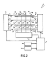
- FIG. 2 schematically shows, by way of nonlimiting example, an alternative plasma panel 1 to which the method of the invention can be applied.
- Panel 1 is of the coplanar maintenance type. It includes column electrodes X1 to X4 orthogonal to pairs P1 to P4 of maintenance electrodes. Each crossing of a column electrode with a pair of electrodes P1 to P4 defines a cell C1 to C16 which represents an elementary image point.
- a cell C1 to C16 which represents an elementary image point.
- only 4 column electrodes X1 to X4 and only 4 pairs P1 to P4 of electrodes are shown which form 4 rows L1 to L4 of cells, but of course, within the framework of the invention, panel 1 may have many more or even fewer of these electrodes.
- Column electrodes X1 to X4 have an addressing function only. They are each connected in a conventional manner to a column 2 addressing device.
- the pairs P1 to P4 of electrodes each comprise a so-called addressing-maintenance electrode Y1 to Y4 and a so-called only maintenance electrode E1 to E4.
- the addressing-maintenance electrodes Y1 to Y4 fulfill an addressing function, in cooperation with the column electrodes X1 to X4, and they fulfill a maintenance function in cooperation with the solely maintenance electrodes E1 to E4 which do not have to fulfill that latter function.
- the maintenance only electrodes E1 to E4 are connected to each other and to a pulse generator 3 from which they all simultaneously receive cyclic voltage slots in order to carry out maintenance cycles.
- the synchronization between the signals applied to the different electrodes is symbolized in FIG. 3 by the presence of a control and synchronization device 6 which is connected to the two addressing devices 2.5 and to the generator 3.
- the panel 1 may optionally further comprise means for controlling the frequency of the maintenance cycles, as already mentioned for the prior art; this way constituting a device 9 for adjusting the luminance of the panel, it is connected to the control and synchronization device 6.
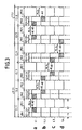
- Figures 3a to 3d are diagrams which illustrate the operation of the panel 1 under the control of the method according to the invention.
- Figure 3a illustrates the operation of the first line L1;
- FIG. 3b illustrates the operation of the second line L2;
- Figures 3c and 3d relate respectively to the third line and the fourth line L3, L4.
- the voltage slots (not shown) applied to the electrodes determine from time t0, simultaneously for all the lines L1 to L4, a succession of n addressing phases PA1, PA2, ...., PAn separated by a maintenance phase PE1 to PE6 (n being equal to 6 in the nonlimiting example described).
- Each addressing phase plus a maintenance phase constitutes a line cycle CL1 to CL6.
- Each addressing phase PA1 to PA6 conventionally comprises a semi-selective operation period CE1 to CE6 for erasing, for example, followed by a selective operation period CI1 to CI6 for registration command.
- the erasing and recording operations for the same line L1 to L4 are separated in time, that is to say that they are carried out in addressing phases PA1 to Different PA6 belonging to different line cycles.
- the first erasure period CE1 begins at time t0 and ends at time t1, and in the non-limiting example described, no addressing is carried out during this period.
- the instant t1 is the start of a first registration period CI1 during which a first AI registration command of the cells belonging to the first line L1 is effectively carried out (a registration command actually carried out is shown in FIGS. 3a to 3d by the fact that the part of the slot which symbolizes the corresponding registration period has hatching).
- the instant t2 is the start of a first maintenance phase PE1 which lasts until an instant t3 where a second addressing phase PA2 begins.
- the time elapsed between time t0 and time t3 corresponds to the duration of the first line cycle CL1, the second addressing phase PA2 begins with a second line cycle CL2.
- the cells of the first line L1 produce light at each maintenance cycle and this as long as they are in the registered state.
- the erasure by semi-selective operation of the first line L1 occurs after a time which corresponds to the frame time, that is to say the time of a line cycle multiplied by the number le lines or in other words this semi-selective erasure occurs just before the registration operation and in the same addressing phase as the latter.
- the erasure of the first line L1 should occur after 4 line cycles, c that is to say in a fifth PA5 addressing phase.
- this erasure can occur earlier: for example it can be carried out in the addressing phase which follows that in which the registration was carried out or in a following addressing phase.
- the semi-selective erase command is carried out during the addressing phase which follows that in which the registration was carried out.
- a semi-selective erase command AE takes place during the second erase period CE2 of the second addressing phase PA2, then thereafter during the sixth erase period CE6 contained in the sixth PA6 addressing phase; an AI registration command having previously been completed during the fifth CI5 registration period of the fifth addressing phase PA5 (an erasing command actually carried out is shown in FIG. 3 by the fact that, the part of the slot which symbolizes the corresponding erasure period includes hatches made in the opposite direction to the hatches which materialize a registration order).
- the selective registration AI takes place during the second registration period C12, and the semi-selective erasure AE takes place during the third erasure period CE3; for the third line L3, the selective registration AI is carried out in a third registration period CI3, and the semi-selective erasure AE is carried out during the fourth erasure period CE4; for the fourth line L4, the selective registration AI takes place in the fourth registration period CI4 and the erasure AE takes place with the fifth erasure period CE5.
- the fifth erasing period CE5 marks the start of a fifth line cycle CL5, and marks the start of a second frame time for the first line L1.
- the semi-selective operation has the function on the one hand to erase all the cells of a line to prepare their possible registration, and has the function on the other hand switching off the lit cells, that is to say registered cells, so as to adjust their luminance by adjusting the duration of a luminance phase PL1, PL2, PL3, PL4 where they are in the registered state; this luminance phase corresponds to the time which separates the first registration period CI1 from the second erasure period CE2, the second registration period CI2 from the third erasure period CE3, etc.
- the amount of light emitted by each of the cells of L1 to L4 is thus proportional to the duration of the luminance phase PL.
- the duration of the luminance phase PL is the minimum duration, it corresponds to the time which separates two consecutive addressing phases PA1, PA2, but the luminance phase can have a longer duration which can reach a frame time.
- a luminance phase PL corresponds to the duration of a line cycle CL1, CL2, ..., CL6
- the luminance phase PL can have a duration equal to N x tCL where N is an integer less than the number n of lines and tCL is the time of a line cycle CL1, CL2, CL3.
- This process can also be combined with the adjustment of the average maintenance frequency, so as to obtain an even greater dynamic.
- the luminance phases PL1 to PL4 have the same duration for the four lines L1 to L4, but it is clear that the method of the invention also applies to confer on the luminance phases of the different lines of different durations at one or more of them.
- the method of the invention applies to all screens which have an internal memory: this is the case of alternative plasma panels, with coplanar maintenance or not; but this is also the case for certain plasma panels of the continuous type as known in particular by IEEE Trans. EI. Dev., Vol. 36, n ° 6, June 1989, pages 1063-1072. This is also the case for certain electroluminescent screens and also the case for liquid crystal screens.
- liquid crystal displays it is true that they are different from the above-mentioned screens in that they do not themselves produce light, but function in transmission and modulate the light of a source. of light in front of which they are placed.
- the method can be applied to liquid crystal screens insofar as it makes it possible to adjust the duration of light transmission in order to adjust the luminance, particularly in the case of liquid crystal screens of an active matrix type, in which each cell incorporates a switching element often formed by a transistor called TFT (from the English expression "THIN-FILM TRANSISTOR").
- TFT from the English expression "THIN-FILM TRANSISTOR”
- the structure of an active matrix liquid crystal screen is shown and described in particular in the review IEEE SPECTRUM September 1989, from page 36 to page 40.
- the TFT In such a liquid crystal screen, the TFT is in the "conductive" or “non-conductive” state depending on the command applied to it. When it is conductive, it lets a signal pass to the liquid crystal cell, which behaves like a capacitor: the capacitor being charged, the signal can disappear without there being a substantial modification of the cell, (i.e. say of the installed electric field), if beforehand the TFT has returned to the "non-conductive"state; the cell in this case has a memory effect.
- the erasure may consist in replacing the cell in the "opaque" state by controlling the conduction of the TFT transistor.
Landscapes
- Engineering & Computer Science (AREA)
- Physics & Mathematics (AREA)
- Computer Hardware Design (AREA)
- General Physics & Mathematics (AREA)
- Theoretical Computer Science (AREA)
- Power Engineering (AREA)
- Plasma & Fusion (AREA)
- Control Of Indicators Other Than Cathode Ray Tubes (AREA)
- Control Of Gas Discharge Display Tubes (AREA)
- Liquid Crystal Display Device Control (AREA)
Applications Claiming Priority (2)
| Application Number | Priority Date | Filing Date | Title |
|---|---|---|---|
| FR9006033A FR2662292B1 (fr) | 1990-05-15 | 1990-05-15 | Procede de reglage de la luminosite d'ecrans de visualisation. |
| FR9006033 | 1990-05-15 |
Publications (2)
| Publication Number | Publication Date |
|---|---|
| EP0457638A1 true EP0457638A1 (de) | 1991-11-21 |
| EP0457638B1 EP0457638B1 (de) | 1995-05-17 |
Family
ID=9396609
Family Applications (1)
| Application Number | Title | Priority Date | Filing Date |
|---|---|---|---|
| EP91401146A Expired - Lifetime EP0457638B1 (de) | 1990-05-15 | 1991-04-30 | Verfahren zur Regelung der Helligkeit von Bildschirmen |
Country Status (5)
| Country | Link |
|---|---|
| US (1) | US5237315A (de) |
| EP (1) | EP0457638B1 (de) |
| JP (1) | JP3098059B2 (de) |
| DE (1) | DE69109742T2 (de) |
| FR (1) | FR2662292B1 (de) |
Cited By (1)
| Publication number | Priority date | Publication date | Assignee | Title |
|---|---|---|---|---|
| FR2713382A1 (fr) * | 1993-12-03 | 1995-06-09 | Thomson Tubes Electroniques | Procédé de réglage de la luminosité globale d'un écran matriciel bistable affichant des demi-teintes. |
Families Citing this family (12)
| Publication number | Priority date | Publication date | Assignee | Title |
|---|---|---|---|---|
| US5684499A (en) * | 1993-11-29 | 1997-11-04 | Nec Corporation | Method of driving plasma display panel having improved operational margin |
| JP3891499B2 (ja) * | 1995-04-14 | 2007-03-14 | パイオニア株式会社 | プラズマディスプレイパネルにおける輝度調整装置 |
| FR2741468B1 (fr) * | 1995-11-17 | 1997-12-12 | Thomson Tubes Electroniques | Procede de commande d'un ecran de visualisation et dispositif de visualisation mettant en oeuvre ce procede |
| FR2744275B1 (fr) | 1996-01-30 | 1998-03-06 | Thomson Csf | Procede de commande d'un panneau de visualisation et dispositif de visualisation utilisant ce procede |
| JP3704813B2 (ja) * | 1996-06-18 | 2005-10-12 | 三菱電機株式会社 | プラズマディスプレイパネルの駆動方法及びプラズマディスプレイ |
| FR2758204B1 (fr) | 1997-01-07 | 1999-04-09 | Thomson Tubes Electroniques | Procede de commande d'adressage d'un panneau a plasma de type alternatif |
| FR2773907B1 (fr) * | 1998-01-20 | 2000-04-07 | Thomson Tubes Electroniques | Panneau a plasma bi-substrat a rendement lumineux ameliore |
| US6271811B1 (en) | 1999-03-12 | 2001-08-07 | Nec Corporation | Method of driving plasma display panel having improved operational margin |
| US6366268B1 (en) | 1999-12-03 | 2002-04-02 | The Trustees Of Princeton University | Display driving method and device |
| FR2812963B1 (fr) * | 2000-08-11 | 2003-07-25 | St Microelectronics Sa | Procede et circuit de commande de cellules d'un ecran a plasma |
| JP4731939B2 (ja) * | 2005-02-10 | 2011-07-27 | パナソニック株式会社 | 表示パネルの駆動方法 |
| CN120091469B (zh) * | 2025-05-07 | 2025-07-22 | 杭州亮晶睛光电科技有限公司 | 一种led警示屏的智能调光系统 |
Citations (2)
| Publication number | Priority date | Publication date | Assignee | Title |
|---|---|---|---|---|
| FR2635902A1 (fr) * | 1988-08-26 | 1990-03-02 | Thomson Csf | Procede de commande tres rapide par adressage semi-selectif et adressage selectif d'un panneau a plasma alternatif a entretien coplanaire |
| FR2635901A1 (fr) * | 1988-08-26 | 1990-03-02 | Thomson Csf | Procede de commande ligne par ligne d'un panneau a plasma du type alternatif a entretien coplanaire |
Family Cites Families (4)
| Publication number | Priority date | Publication date | Assignee | Title |
|---|---|---|---|---|
| US4611203A (en) * | 1984-03-19 | 1986-09-09 | International Business Machines Corporation | Video mode plasma display |
| US4683470A (en) * | 1985-03-05 | 1987-07-28 | International Business Machines Corporation | Video mode plasma panel display |
| US5059963A (en) * | 1988-01-12 | 1991-10-22 | Sharp Kabushiki Kaisha | Two-level display device with hatching control means |
| US4984218A (en) * | 1990-04-26 | 1991-01-08 | Mobil Oil Corporation | Marine acoustic array configured for tow noise reduction |
-
1990
- 1990-05-15 FR FR9006033A patent/FR2662292B1/fr not_active Expired - Lifetime
-
1991
- 1991-04-26 US US07/691,781 patent/US5237315A/en not_active Expired - Fee Related
- 1991-04-30 EP EP91401146A patent/EP0457638B1/de not_active Expired - Lifetime
- 1991-04-30 DE DE69109742T patent/DE69109742T2/de not_active Expired - Fee Related
- 1991-05-15 JP JP03139579A patent/JP3098059B2/ja not_active Expired - Fee Related
Patent Citations (2)
| Publication number | Priority date | Publication date | Assignee | Title |
|---|---|---|---|---|
| FR2635902A1 (fr) * | 1988-08-26 | 1990-03-02 | Thomson Csf | Procede de commande tres rapide par adressage semi-selectif et adressage selectif d'un panneau a plasma alternatif a entretien coplanaire |
| FR2635901A1 (fr) * | 1988-08-26 | 1990-03-02 | Thomson Csf | Procede de commande ligne par ligne d'un panneau a plasma du type alternatif a entretien coplanaire |
Cited By (2)
| Publication number | Priority date | Publication date | Assignee | Title |
|---|---|---|---|---|
| FR2713382A1 (fr) * | 1993-12-03 | 1995-06-09 | Thomson Tubes Electroniques | Procédé de réglage de la luminosité globale d'un écran matriciel bistable affichant des demi-teintes. |
| US6181306B1 (en) | 1993-12-03 | 2001-01-30 | Thomson Tubes Electroniques | Method for adjusting the overall luminosity of a bistable matrix screen displaying half-tones |
Also Published As
| Publication number | Publication date |
|---|---|
| EP0457638B1 (de) | 1995-05-17 |
| DE69109742T2 (de) | 1995-09-14 |
| DE69109742D1 (de) | 1995-06-22 |
| JP3098059B2 (ja) | 2000-10-10 |
| FR2662292B1 (fr) | 1992-07-24 |
| JPH04229897A (ja) | 1992-08-19 |
| US5237315A (en) | 1993-08-17 |
| FR2662292A1 (fr) | 1991-11-22 |
Similar Documents
| Publication | Publication Date | Title |
|---|---|---|
| EP0356313B1 (de) | Verfahren zur sehr schnellen Ansteuerung einer wechselspannungsbetriebenen Plasmaanzeigetafel mit koplanarer Unterstützung durch halbselektive Adressierung und selektive Adressierung | |
| EP0357485B1 (de) | Zeile-pro-Zeile-Ansteuerverfahren einer Plasmaanzeigetafel vom wechselspannungsbetriebenen Typ mit koplanarer Unterstützung | |
| EP0457638B1 (de) | Verfahren zur Regelung der Helligkeit von Bildschirmen | |
| FR2535498A1 (fr) | Procede et dispositif d'affichage par plasma | |
| EP0361992B1 (de) | Plasma-Anzeigeplatte mit modifizierter Adressierbarkeit | |
| FR2755784A1 (fr) | Procede de pilotage d'un panneau d'affichage dans un plasma | |
| FR2925745A1 (fr) | Afficheur a cristaux liquides et son procede de pilotage | |
| JPH05249434A (ja) | 強誘電性液晶デバイス | |
| JP5216022B2 (ja) | 空間光変調器 | |
| EP0279746A1 (de) | Plasmapaneel mit vier Elektroden pro Elementarbildpunkt und Verfahren zur Steuerung eines solchen Plasmapaneeles | |
| EP0278194B1 (de) | Elektrolumineszenzanzeige mit Speichereffekt, gesteuert durch mehrfache phasenverschobene Auffrischspannungen | |
| EP0774746A1 (de) | Steuerverfahren für eine Anzeigetafel und Anzeigetafel zur Durchführung dieses Verfahrens | |
| US4839563A (en) | Pulse burst panel drive for electroluminescent displays | |
| EP0907945B1 (de) | Verfahren zum aktivieren von bildschirmzellen und anzeigegerät zur durchführung dieses verfahrens | |
| EP0951711B1 (de) | Verfahren zur adressierungsansteurung einer wechselstromplasmaanzeigetafel | |
| EP0817232B1 (de) | Verfahren zur Regenerierung von Mikrospitzen einer flachen Anzeigetafel | |
| FR2629245A1 (fr) | Procede de commande point par point d'un panneau a plasma | |
| CN1036097A (zh) | 对数据存贮元件进行寻址的方法及其装置 | |
| FR2713382A1 (fr) | Procédé de réglage de la luminosité globale d'un écran matriciel bistable affichant des demi-teintes. | |
| FR2769115A1 (fr) | Procede de commande d'un panneau de visualisation alternatif integrant une ionisation | |
| EP1479062A1 (de) | Einrichtung zür stromversorgung und steuerung einer plasmaanzeigetafel mit transformatoren | |
| FR2662291A1 (fr) | Procede de reglage de la luminance d'un panneau a plasma alternatif. | |
| FR2744275A1 (fr) | Procede de commande d'un panneau de visualisation et dispositif de visualisation utilisant ce procede | |
| FR2795218A1 (fr) | Procede d'adressage d'un panneau de visualisation a effet memoire | |
| FR2790861A1 (fr) | Dispositif d'attaque pour dispositif luminescent a emission par effet de champ |
Legal Events
| Date | Code | Title | Description |
|---|---|---|---|
| PUAI | Public reference made under article 153(3) epc to a published international application that has entered the european phase |
Free format text: ORIGINAL CODE: 0009012 |
|
| AK | Designated contracting states |
Kind code of ref document: A1 Designated state(s): DE FR GB |
|
| 17P | Request for examination filed |
Effective date: 19911220 |
|
| 17Q | First examination report despatched |
Effective date: 19940118 |
|
| GRAA | (expected) grant |
Free format text: ORIGINAL CODE: 0009210 |
|
| AK | Designated contracting states |
Kind code of ref document: B1 Designated state(s): DE FR GB |
|
| REF | Corresponds to: |
Ref document number: 69109742 Country of ref document: DE Date of ref document: 19950622 |
|
| GBT | Gb: translation of ep patent filed (gb section 77(6)(a)/1977) |
Effective date: 19950627 |
|
| PLBE | No opposition filed within time limit |
Free format text: ORIGINAL CODE: 0009261 |
|
| STAA | Information on the status of an ep patent application or granted ep patent |
Free format text: STATUS: NO OPPOSITION FILED WITHIN TIME LIMIT |
|
| 26N | No opposition filed | ||
| REG | Reference to a national code |
Ref country code: GB Ref legal event code: IF02 |
|
| PGFP | Annual fee paid to national office [announced via postgrant information from national office to epo] |
Ref country code: GB Payment date: 20030314 Year of fee payment: 13 |
|
| PGFP | Annual fee paid to national office [announced via postgrant information from national office to epo] |
Ref country code: FR Payment date: 20030424 Year of fee payment: 13 |
|
| PGFP | Annual fee paid to national office [announced via postgrant information from national office to epo] |
Ref country code: DE Payment date: 20030507 Year of fee payment: 13 |
|
| PG25 | Lapsed in a contracting state [announced via postgrant information from national office to epo] |
Ref country code: GB Free format text: LAPSE BECAUSE OF NON-PAYMENT OF DUE FEES Effective date: 20040430 |
|
| PG25 | Lapsed in a contracting state [announced via postgrant information from national office to epo] |
Ref country code: DE Free format text: LAPSE BECAUSE OF NON-PAYMENT OF DUE FEES Effective date: 20041103 |
|
| GBPC | Gb: european patent ceased through non-payment of renewal fee |
Effective date: 20040430 |
|
| PG25 | Lapsed in a contracting state [announced via postgrant information from national office to epo] |
Ref country code: FR Free format text: LAPSE BECAUSE OF NON-PAYMENT OF DUE FEES Effective date: 20041231 |
|
| REG | Reference to a national code |
Ref country code: FR Ref legal event code: ST |