EP0457932A1 - Arrangement de circuit pour la commutation de bande dans un tuner - Google Patents
Arrangement de circuit pour la commutation de bande dans un tuner Download PDFInfo
- Publication number
- EP0457932A1 EP0457932A1 EP90109584A EP90109584A EP0457932A1 EP 0457932 A1 EP0457932 A1 EP 0457932A1 EP 90109584 A EP90109584 A EP 90109584A EP 90109584 A EP90109584 A EP 90109584A EP 0457932 A1 EP0457932 A1 EP 0457932A1
- Authority
- EP
- European Patent Office
- Prior art keywords
- terminal
- switching
- circuit arrangement
- potential terminal
- mos
- Prior art date
- Legal status (The legal status is an assumption and is not a legal conclusion. Google has not performed a legal analysis and makes no representation as to the accuracy of the status listed.)
- Granted
Links
- 230000003321 amplification Effects 0.000 claims abstract description 5
- 238000003199 nucleic acid amplification method Methods 0.000 claims abstract description 5
- 230000008878 coupling Effects 0.000 claims description 5
- 238000010168 coupling process Methods 0.000 claims description 5
- 238000005859 coupling reaction Methods 0.000 claims description 5
- 230000001681 protective effect Effects 0.000 claims description 2
- 239000003990 capacitor Substances 0.000 description 3
- 230000000694 effects Effects 0.000 description 1
Images

Classifications
-
- H—ELECTRICITY
- H03—ELECTRONIC CIRCUITRY
- H03J—TUNING RESONANT CIRCUITS; SELECTING RESONANT CIRCUITS
- H03J5/00—Discontinuous tuning; Selecting predetermined frequencies; Selecting frequency bands with or without continuous tuning in one or more of the bands, e.g. push-button tuning, turret tuner
- H03J5/24—Discontinuous tuning; Selecting predetermined frequencies; Selecting frequency bands with or without continuous tuning in one or more of the bands, e.g. push-button tuning, turret tuner with a number of separate pretuned tuning circuits or separate tuning elements selectively brought into circuit, e.g. for waveband selection or for television channel selection
- H03J5/242—Discontinuous tuning; Selecting predetermined frequencies; Selecting frequency bands with or without continuous tuning in one or more of the bands, e.g. push-button tuning, turret tuner with a number of separate pretuned tuning circuits or separate tuning elements selectively brought into circuit, e.g. for waveband selection or for television channel selection used exclusively for band selection
- H03J5/244—Discontinuous tuning; Selecting predetermined frequencies; Selecting frequency bands with or without continuous tuning in one or more of the bands, e.g. push-button tuning, turret tuner with a number of separate pretuned tuning circuits or separate tuning elements selectively brought into circuit, e.g. for waveband selection or for television channel selection used exclusively for band selection using electronic means
Definitions
- the invention relates to a circuit arrangement for range switching in tuners with the features of the preamble of claim 1.
- Television tuners usually contain two or three tuners that are operated electrically largely independently of one another and cover the television frequency ranges in the VHF bands and in the UHF band.
- Hyperband tuners i.e. tuners that also cover the hyperband distributed in cable networks with the frequency range 300 to 470 MHz, generally consist of three electrically independent sub-tuners.
- the band or range switching of the tuned resonant circuits is generally not carried out with switch diodes because of the large frequency ranges to be tuned.
- switch diodes are used directly at the antenna input, which only switch the currently selected area to the antenna connection of the television set. The switchover of the tuners and the switch diodes takes place - as described above - by means of switch transistors.
- an integrated circuit which contains a mixer and an oscillator for each sub-area.
- a switching device is also integrated into this integrated circuit, which switches on the desired mixer and oscillator by applying a specific control signal, for example voltage level.
- the control signal can be derived, for example, from appropriately designed voltage dividers from switched-over operating voltages for the part tuners.
- the switch transistors only switch the current of the switch diodes and the operating voltage of the pre-stages of the tuner, into which MOS tetrodes are usually used to amplify the high frequency.
- Two circuit arrangements for area switching in television tuners with MOS tetrodes and an integrated circuit for VHF / UHF switching are shown, for example, on pages 767 and 768 of the Siemens data book 1986/87 "ICs for Consumer Electronics".
- a hyperband tuner known as Philips UV 816 which does not require switch transistors. This is achieved by an integrated switching device with non-current-limited switching outputs, via which the first gate connections of the non-switched-on MOS tetrodes are switched to ground. As a result, these MOS tetrodes become currentless and lose their amplification. Only the MOS tetrode of the active area remains switched on, since the switching output of the integrated switching device provided for this remains high-resistance and thus inactive. The disadvantage of this principle is: Such a tuner requires a control device for its control, that is, for. B.
- the invention is therefore based on the object of specifying a circuit arrangement for range switching in tuners which is functionally and software-compatible with the previous tuners and whose circuit complexity and space requirement is reduced compared to the previously known circuits.
- the input stage has three preliminary stages 1, 1 ′ and 1 ′′ with MOS tetrodes 4 for amplifying an antenna signal to be applied to a terminal 20.
- this antenna signal Via a coupling member 21, for. B. a coupling capacitor, this antenna signal reaches the Cathodes of three switch diodes 37, 37 'and 37'', the anodes of which are connected to an input terminal 7, 7', 7 '' of the preliminary stages 1, 1 'and 1''.
- At their output terminals 8, 8 'and 8''a high frequency amplified signal can be tapped for each area of the respective preamplifier 1, 1' and 1 ''.
- preliminary stage 1 for a first area, here z. B. the VHF I area with its individual circuit components shown in detail, as they are known from the Siemens data book 1986/87 mentioned above. The circuit arrangement is therefore only dealt with in the following to the extent that it is necessary for an understanding of the invention.
- the source connection S of the MOS tetrode 4 is connected to the connection point of a first voltage divider 15 and the first gate connection G1 is connected to the connection point of a second voltage divider 16 for setting the operating point.
- Both voltage dividers 15 and 16 are located between a reference potential terminal 6 and a terminal 43, which can be switched via a pnp switching transistor 40 to a supply potential terminal 5 with an applied positive voltage.
- the collector connection of this pnp switching transistor 40 with the terminal 43 and its base connection is connected via a base resistor 42 to a switching output 14 of a switching device 9.
- the emitter connection of the pnp switching transistor 40 is connected on the one hand via an emitter resistor 41 to the base connection of the pnp switching transistor 40 and on the other hand to the supply potential terminal 5.
- the switching output 14 of the switching device 9 is controlled via one or more control connections 11 by means of one or more control signals.
- the anode of the switch diode 37 is connected to the terminal 43 of the preliminary stage 1 via a resistor 39.
- the switching output 14 of the switching device 9 is switched to low impedance when the VHF I range is selected by operating elements in the television set, that is to say to reference potential, the pnp switching transistor switches 40 a.
- the positive voltage at the supply potential terminal 5 thus reaches the terminal 43, as a result of which the preliminary stage 1 is connected to the positive voltage and is thus activated.
- the switch diode 37 becomes conductive since its cathode is now more negative than its anode.
- the current for switching this switch diode 37 is provided by the pnp switching transistor 40.
- the antenna signal present at the terminal 20 and to be amplified is thus amplified in the preamplifier 1 and is available at the output terminal 8.
- Switching to the other areas, here the two pre-stages 1 'and 1' 'for the VHF II and UHF areas, is carried out in an analogous manner via the switching outputs 14' and 14 '' of the switching device 9, as well as by means of the Reference numerals 7 ', 37', 40 ', 41', 42 'and 43' and 7 '', 37 '', 40 '', 41 '', 42 '' and 43 '' designated circuit components is shown.
- the same digits of the reference symbols denote analog switching elements.
- preamplifier 1' With low-impedance switching output 14 ', preamplifier 1' thus becomes active, while with low-impedance switching output 14 '', preamplifier 1 '' is connected to supply potential terminal 5 via the then switched on pnp switching transistor 40 '' and thus works as an amplifier.
- the switching outputs 14, 14 'and 14' 'of the switching device 9 are current-limited open collector outputs.
- a current limitation in the switching device 9 prevents the base current of the pnp switching transistors 40, 40 'and 40' 'from being too high.
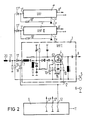
- FIG. 2 shows an exemplary embodiment of a circuit arrangement according to the invention for range switching in tuners.
- the same reference numerals as in FIG 1 indicate the same circuit elements.
- the source terminal S of the MOS tetrode 4 is connected via a resistor 10 and the terminal 2 to a switching output 12 of the switching device 9.
- this switching output 12 of the switching device 9 can be switched to reference potential and thus connected to the reference potential terminal 6, whereby the MOS tetrode 4 and thus the preliminary stage 1 can be activated is.
- the MOS tetrode 4 So that the MOS tetrode 4 is switched off when the switching output 12 is not at reference potential, two voltage dividers which are matched to one another and connected between the supply potential terminal 5 and the reference potential terminal 6 are connected to the MOS tetrode 4.
- the first voltage divider 15, for example consisting of two resistors, is connected with its connection point to the source connection S and the second voltage divider 16, for example consisting of two resistors, is connected with its connection point to a first gate connection G1 of the MOS tetrode 4.
- the first voltage divider 15 and second voltage divider 16 are set so that a negative voltage is reached at the source terminal S of the MOS tetrode 4, which is large enough on the one hand to pinch off a channel forming in the MOS tetrode 4 and on the other hand below the response threshold of protective diodes connected to the first gate terminal G1 and second gate terminal G2 of the MOS tetrode 4 remains.
- the MOS tetrode 4 is currentless and RF amplification is not possible.
- the pre-stage 1 is to be activated, the switching output 12 of the switching device 9 is switched to reference potential in accordance with one or more control signals to be applied to one or more input terminals 11 of the switching device 9 and thus the source connection S of the MOS tetrode 4 via the resistor 10 with the Reference potential terminal 6 connected.
- This resistor 10, which is connected in parallel with a resistor of the first voltage divider 15, is advantageously dimensioned such that the operating point of the MOS tetrode 4 provided for optimum amplification is established.
- the aforementioned switch diode 17 is provided and connected with its cathode to the input terminal 7 of the preamplifier 1 and via a resistor 18, which is high-ohmic in comparison to the input impedance of the preamplifier 1, to the switching output 12 of the switching device 9 is connected and that a third voltage divider 19 connected between the supply potential terminal 5 and reference potential terminal 6 is provided, which is connected with its connection point to the anode of the switch diode 17.
- This measure has the effect that - as long as the switching output 12 is not at reference potential - the switch diode 17 blocks and therefore no antenna signal reaches the input terminal 7 of the preamplifier 1.
- the switch diode 17 blocks this area since the anode of the switch diode 17 is more negative than the cathode due to the third voltage divider 19, which is connected via a resistor 18 connected between the cathode of the switch diode 17 and the switching output 12 and the resistor 10 at the source connection S of the MOS Tetrode 4 lies.
- switch diode 17 carries current since its anode potential becomes more positive than its cathode potential.
- the further pre-stages 1 'and 1''of the remaining areas provided in the tuner can - as shown in FIG. 2 - be connected in the same way to further switching outputs 12' and 12 '' of the switching device 9 and to via further switch diodes 17 'and 17'' the coupling capacitor 21 of the antenna input terminal 20 are switched.
- the switching outputs 12 'and 12'' are to be connected to the terminals 2' and 2 '' of the preamplifiers 1 'and 1'', which in turn are each connected via a resistor to the source connection of the respective MOS tetrode of the preamplifiers 1' and 1 '' are connected.
- An integrated circuit is particularly suitable as the switching device 9, the switching outputs 12, 12 ′ and 12 ′′ necessary for the range switching need not have any current limitation. It is particularly advantageous that the control of the switching outputs 12, 12 'and 12' 'can be designed to be compatible with the control software of the previous tuners.
- the switching device 9 can also be included, for example, in an integrated PLL (phase-locked-loop) circuit which, for. B. has all the stages necessary for frequency adjustment and band switching.
- switching transistors provided in the switching device 9 for driving the switching outputs 12, 12 'and 12' ' should be dimensioned such that they can switch a current of about 25 mA at a dielectric strength of about 12 V.
- the principle of the present invention and thus the switching off of a preliminary stage via the source potential of a MOS tetrode is suitable for all tuners, in particular those with VHF resonant circuits which can be switched over with switch diodes but also those which work without switch diodes.
- the most important advantage of the invention lies in the fact that the circuit arrangement for switching the range of the tuner to the previous circuit arrangements is functionally and software-compatible and its circuit complexity and space requirements are reduced compared to the previously known circuit arrangements.
Landscapes
- Input Circuits Of Receivers And Coupling Of Receivers And Audio Equipment (AREA)
- Channel Selection Circuits, Automatic Tuning Circuits (AREA)
- Circuits Of Receivers In General (AREA)
- Pharmaceuticals Containing Other Organic And Inorganic Compounds (AREA)
- Circuit For Audible Band Transducer (AREA)
- Networks Using Active Elements (AREA)
- Oscillators With Electromechanical Resonators (AREA)
- Amplifiers (AREA)
- Electronic Switches (AREA)
Priority Applications (14)
| Application Number | Priority Date | Filing Date | Title |
|---|---|---|---|
| ES90109584T ES2075089T3 (es) | 1990-05-21 | 1990-05-21 | Disposicion de circuito para la conmutacion de zona en sintonizadores. |
| AT90109584T ATE126412T1 (de) | 1990-05-21 | 1990-05-21 | Schaltungsanordnung zur bereichsumschaltung in tunern. |
| EP90109584A EP0457932B1 (fr) | 1990-05-21 | 1990-05-21 | Arrangement de circuit pour la commutation de bande dans un tuner |
| DE59009512T DE59009512D1 (de) | 1990-05-21 | 1990-05-21 | Schaltungsanordnung zur Bereichsumschaltung in Tunern. |
| YU46891A YU46891A (sh) | 1990-05-21 | 1991-03-13 | Sklop kola za promenu opsega kod tjunera |
| SI9110468A SI9110468A (sl) | 1990-05-21 | 1991-03-13 | Vezje za preklapljanje od območja na območje v postajnikih |
| PL91290170A PL165175B1 (pl) | 1990-05-21 | 1991-05-08 | Uklad przelaczania zakresów glowicy PL |
| TR91/0501A TR25666A (tr) | 1990-05-21 | 1991-05-17 | AYARLAYICI KISIMLARDA MERTEBE DEGISIMI ICIN DEVRE DüZENI |
| FI912441A FI912441A7 (fi) | 1990-05-21 | 1991-05-20 | Piirijärjestely virittimen alueen vaihtamiseksi |
| US07/703,197 US5204645A (en) | 1990-05-21 | 1991-05-20 | Circuit configuration for range switching in tuners |
| SU914895282A RU2077115C1 (ru) | 1990-05-21 | 1991-05-20 | Устройство для переключения диапазона в тьюнерах |
| JP14544491A JP3174089B2 (ja) | 1990-05-21 | 1991-05-20 | チューナの範囲切換用回路装置 |
| LVP-93-512A LV10988B (en) | 1990-05-21 | 1993-06-08 | Circuit arrangement for band switching in tuners |
| LTIP1565A LT3635B (en) | 1990-05-21 | 1993-12-08 | Switching scheme for diapasons in tuner |
Applications Claiming Priority (1)
| Application Number | Priority Date | Filing Date | Title |
|---|---|---|---|
| EP90109584A EP0457932B1 (fr) | 1990-05-21 | 1990-05-21 | Arrangement de circuit pour la commutation de bande dans un tuner |
Publications (2)
| Publication Number | Publication Date |
|---|---|
| EP0457932A1 true EP0457932A1 (fr) | 1991-11-27 |
| EP0457932B1 EP0457932B1 (fr) | 1995-08-09 |
Family
ID=8204006
Family Applications (1)
| Application Number | Title | Priority Date | Filing Date |
|---|---|---|---|
| EP90109584A Expired - Lifetime EP0457932B1 (fr) | 1990-05-21 | 1990-05-21 | Arrangement de circuit pour la commutation de bande dans un tuner |
Country Status (13)
| Country | Link |
|---|---|
| US (1) | US5204645A (fr) |
| EP (1) | EP0457932B1 (fr) |
| JP (1) | JP3174089B2 (fr) |
| AT (1) | ATE126412T1 (fr) |
| DE (1) | DE59009512D1 (fr) |
| ES (1) | ES2075089T3 (fr) |
| FI (1) | FI912441A7 (fr) |
| LT (1) | LT3635B (fr) |
| LV (1) | LV10988B (fr) |
| PL (1) | PL165175B1 (fr) |
| RU (1) | RU2077115C1 (fr) |
| TR (1) | TR25666A (fr) |
| YU (1) | YU46891A (fr) |
Cited By (12)
| Publication number | Priority date | Publication date | Assignee | Title |
|---|---|---|---|---|
| EP0769850A1 (fr) * | 1995-10-17 | 1997-04-23 | Philips Patentverwaltung GmbH | Etage d'entrée haute fréquence |
| GB2316250A (en) * | 1996-08-09 | 1998-02-18 | Alps Electric Co Ltd | TV band selection with resistor for adjusting Q |
| WO1998015055A1 (fr) * | 1996-09-30 | 1998-04-09 | Siemens Aktiengesellschaft | Circuit preamplificateur multiple pour dispositif d'accord de television |
| EP0851580A1 (fr) * | 1996-12-26 | 1998-07-01 | SHARP Corporation | Circuit d'accord pour un modem pour câble |
| WO1999057809A1 (fr) * | 1998-04-30 | 1999-11-11 | Infineon Technologies Ag | Circuit pour selection de gammes dans des recepteurs haute frequence |
| US6131023A (en) * | 1997-10-24 | 2000-10-10 | Sharp Kabushiki Kaisha | Cable modem tuner with an up-stream and a reception circuit in the same casing |
| WO2001022583A3 (fr) * | 1999-09-22 | 2002-01-24 | Thomson Licensing Sa | Boucle a asservissement de phase a memoire pour alignements electroniques |
| EP1213837A1 (fr) * | 2000-11-29 | 2002-06-12 | Alps Electric Co., Ltd. | Circuit d'accord pour la réception de signaux de télévision dans les bandes VHF et UHF |
| US6452645B1 (en) | 1997-09-29 | 2002-09-17 | Infineon Technologies Ag | Multiple preliminary stage circuit for television tuner |
| EP1263138A1 (fr) * | 2001-05-31 | 2002-12-04 | Alps Electric Co., Ltd. | Circuit d'accord de télévision |
| US6714068B2 (en) | 1999-06-30 | 2004-03-30 | Infineon Technologies Ag | Circuit configuration with selectively operating amplifiers |
| EP1265360B2 (fr) † | 2001-06-08 | 2012-08-15 | Alps Electric Co., Ltd. | Circuit d' accord de télévision intégré comprenant un circuit pour la commutation de bande |
Families Citing this family (4)
| Publication number | Priority date | Publication date | Assignee | Title |
|---|---|---|---|---|
| US5774017A (en) * | 1996-06-03 | 1998-06-30 | Anadigics, Inc. | Multiple-band amplifier |
| JP2002501715A (ja) * | 1998-03-13 | 2002-01-15 | コーニンクレッカ フィリップス エレクトロニクス エヌ ヴィ | ダイオード検知器を使う同調 |
| EP1156582A3 (fr) * | 2000-05-16 | 2004-04-28 | Nokia Corporation | Optimalisation d'impédance d'une chaíne de transmission et de réception |
| US7149483B1 (en) | 2003-10-28 | 2006-12-12 | Magnolia Broadband Inc. | Amplifying diversity signals using power amplifiers |
Citations (2)
| Publication number | Priority date | Publication date | Assignee | Title |
|---|---|---|---|---|
| US4442548A (en) * | 1982-05-14 | 1984-04-10 | Rca Corporation | Television receiver tuning circuit tunable over a wide frequency range |
| EP0299578A1 (fr) * | 1987-07-13 | 1989-01-18 | Koninklijke Philips Electronics N.V. | Circuit d'entrée H.F. de télévision |
Family Cites Families (4)
| Publication number | Priority date | Publication date | Assignee | Title |
|---|---|---|---|---|
| US4048598A (en) * | 1976-05-28 | 1977-09-13 | Rca Corporation | Uhf tuning circuit utilizing a varactor diode |
| JPS6121882Y2 (fr) * | 1980-11-14 | 1986-07-01 | ||
| JPS58166134U (ja) * | 1982-04-28 | 1983-11-05 | アルプス電気株式会社 | 電子同調チユ−ナ |
| DE3633384A1 (de) * | 1986-10-01 | 1988-04-14 | Telefunken Electronic Gmbh | Fernsehtuner fuer drei unterschiedliche frequenzbereiche |
-
1990
- 1990-05-21 DE DE59009512T patent/DE59009512D1/de not_active Expired - Lifetime
- 1990-05-21 EP EP90109584A patent/EP0457932B1/fr not_active Expired - Lifetime
- 1990-05-21 ES ES90109584T patent/ES2075089T3/es not_active Expired - Lifetime
- 1990-05-21 AT AT90109584T patent/ATE126412T1/de not_active IP Right Cessation
-
1991
- 1991-03-13 YU YU46891A patent/YU46891A/sh unknown
- 1991-05-08 PL PL91290170A patent/PL165175B1/pl unknown
- 1991-05-17 TR TR91/0501A patent/TR25666A/xx unknown
- 1991-05-20 RU SU914895282A patent/RU2077115C1/ru active
- 1991-05-20 US US07/703,197 patent/US5204645A/en not_active Expired - Lifetime
- 1991-05-20 FI FI912441A patent/FI912441A7/fi not_active Application Discontinuation
- 1991-05-20 JP JP14544491A patent/JP3174089B2/ja not_active Expired - Lifetime
-
1993
- 1993-06-08 LV LVP-93-512A patent/LV10988B/lv unknown
- 1993-12-08 LT LTIP1565A patent/LT3635B/lt not_active IP Right Cessation
Patent Citations (2)
| Publication number | Priority date | Publication date | Assignee | Title |
|---|---|---|---|---|
| US4442548A (en) * | 1982-05-14 | 1984-04-10 | Rca Corporation | Television receiver tuning circuit tunable over a wide frequency range |
| EP0299578A1 (fr) * | 1987-07-13 | 1989-01-18 | Koninklijke Philips Electronics N.V. | Circuit d'entrée H.F. de télévision |
Non-Patent Citations (1)
| Title |
|---|
| "ICs für die Unterhaltungselektronik" 1986, Siemens, DE * |
Cited By (17)
| Publication number | Priority date | Publication date | Assignee | Title |
|---|---|---|---|---|
| EP0769850A1 (fr) * | 1995-10-17 | 1997-04-23 | Philips Patentverwaltung GmbH | Etage d'entrée haute fréquence |
| GB2316250A (en) * | 1996-08-09 | 1998-02-18 | Alps Electric Co Ltd | TV band selection with resistor for adjusting Q |
| GB2316250B (en) * | 1996-08-09 | 2000-09-06 | Alps Electric Co Ltd | Television tuner |
| WO1998015055A1 (fr) * | 1996-09-30 | 1998-04-09 | Siemens Aktiengesellschaft | Circuit preamplificateur multiple pour dispositif d'accord de television |
| US6160572A (en) * | 1996-12-26 | 2000-12-12 | Sharp Kabushiki Kaisha | Tuner for cable modem |
| EP0851580A1 (fr) * | 1996-12-26 | 1998-07-01 | SHARP Corporation | Circuit d'accord pour un modem pour câble |
| US6452645B1 (en) | 1997-09-29 | 2002-09-17 | Infineon Technologies Ag | Multiple preliminary stage circuit for television tuner |
| US6131023A (en) * | 1997-10-24 | 2000-10-10 | Sharp Kabushiki Kaisha | Cable modem tuner with an up-stream and a reception circuit in the same casing |
| WO1999057809A1 (fr) * | 1998-04-30 | 1999-11-11 | Infineon Technologies Ag | Circuit pour selection de gammes dans des recepteurs haute frequence |
| DE19819544A1 (de) * | 1998-04-30 | 1999-11-11 | Siemens Ag | Schaltungsanordnung zur Bereichsumschaltung in Hochfrequenzempfängern |
| US6751449B1 (en) | 1998-04-30 | 2004-06-15 | Infineon Technologies Ag | Circuit configuration for band changeover in high-frequency receivers |
| US6714068B2 (en) | 1999-06-30 | 2004-03-30 | Infineon Technologies Ag | Circuit configuration with selectively operating amplifiers |
| WO2001022583A3 (fr) * | 1999-09-22 | 2002-01-24 | Thomson Licensing Sa | Boucle a asservissement de phase a memoire pour alignements electroniques |
| EP1213837A1 (fr) * | 2000-11-29 | 2002-06-12 | Alps Electric Co., Ltd. | Circuit d'accord pour la réception de signaux de télévision dans les bandes VHF et UHF |
| US6903783B2 (en) | 2000-11-29 | 2005-06-07 | Alps Electric Co., Ltd. | Tuner for receiving television signal in VHF band and UHF band |
| EP1263138A1 (fr) * | 2001-05-31 | 2002-12-04 | Alps Electric Co., Ltd. | Circuit d'accord de télévision |
| EP1265360B2 (fr) † | 2001-06-08 | 2012-08-15 | Alps Electric Co., Ltd. | Circuit d' accord de télévision intégré comprenant un circuit pour la commutation de bande |
Also Published As
| Publication number | Publication date |
|---|---|
| FI912441A0 (fi) | 1991-05-20 |
| JPH04230114A (ja) | 1992-08-19 |
| JP3174089B2 (ja) | 2001-06-11 |
| DE59009512D1 (de) | 1995-09-14 |
| RU2077115C1 (ru) | 1997-04-10 |
| FI912441L (fi) | 1991-11-22 |
| LV10988B (en) | 1996-04-20 |
| LTIP1565A (en) | 1995-06-26 |
| TR25666A (tr) | 1993-07-01 |
| ES2075089T3 (es) | 1995-10-01 |
| PL165175B1 (pl) | 1994-11-30 |
| EP0457932B1 (fr) | 1995-08-09 |
| ATE126412T1 (de) | 1995-08-15 |
| US5204645A (en) | 1993-04-20 |
| LT3635B (en) | 1996-01-25 |
| YU46891A (sh) | 1994-06-10 |
| FI912441A7 (fi) | 1991-11-22 |
| LV10988A (lv) | 1995-12-20 |
Similar Documents
| Publication | Publication Date | Title |
|---|---|---|
| EP0457932B1 (fr) | Arrangement de circuit pour la commutation de bande dans un tuner | |
| DE2412689C3 (de) | Schaltungsanordnung zur Abstimmung und Bereichs- bzw. Bandumschaltung eines HF-Schwingungskreises | |
| DE3318536A1 (de) | Durchstimmbare schaltungsanordnung | |
| DE3875661T2 (de) | Fernseh-hf-eingangsschaltung. | |
| DE2836288C2 (de) | Kombi-Tuner | |
| DE2213484B2 (de) | Hochfrequenter Breitbandverstärker | |
| DE69332448T2 (de) | Abstimmschaltung für Fernsehempfänger | |
| EP0193995B1 (fr) | Agencement de circuit pour un tuner pour la commutation de plusieurs bandes de fréquence | |
| EP0457934B1 (fr) | Arrangement de circuit pour la commutation de bande dans un tuner | |
| DE3751830T2 (de) | Tuner mit FET | |
| DE3689704T2 (de) | Steuerbarer Oszillator. | |
| DE3752195T2 (de) | Abstimmbarer Oszillator mit Dual-Gate-FET | |
| DE60222607T3 (de) | Integrierter Fernsehtuner mit Schaltungsanordnung zur Bereichsumschaltung | |
| DE2812991B2 (de) | Frequenzteilerschaltung für einen Fernsehtuner | |
| EP0429914A2 (fr) | Circuit d'accord | |
| DE3539379C2 (de) | Monolithisch integrierte Steuerschaltung für die Umschaltung von Transistoren | |
| EP0929936B1 (fr) | Circuit preamplificateur multiple pour dispositif d'accord de television | |
| EP1078456B1 (fr) | Circuit pour selection de gammes dans des recepteurs haute frequence | |
| DE9005774U1 (de) | Schaltungsanordnung für Bereichsumschaltung in Tunern | |
| DE3341499C2 (de) | VHF-Tuner | |
| DE3144390A1 (de) | Schwingkreisschaltung | |
| DE2918636A1 (de) | Schaltungsanordnung mit in einem grossen frequenzbereich abstimmbaren und an eine transistorstufe gekoppelten hf- schwingkreis fuer fernsehgeraete | |
| DE3144242C2 (fr) | ||
| EP0277693B1 (fr) | Montage d'un mélangeur dans un circuit d'accord HF | |
| EP0348698B1 (fr) | Circuit d'entrée d'un tuner pour récepteur de télévision |
Legal Events
| Date | Code | Title | Description |
|---|---|---|---|
| PUAI | Public reference made under article 153(3) epc to a published international application that has entered the european phase |
Free format text: ORIGINAL CODE: 0009012 |
|
| 17P | Request for examination filed |
Effective date: 19901205 |
|
| AK | Designated contracting states |
Kind code of ref document: A1 Designated state(s): AT BE CH DE DK ES FR GB GR IT LI LU NL SE |
|
| RBV | Designated contracting states (corrected) |
Designated state(s): AT BE DE ES FR GB IT NL SE |
|
| 17Q | First examination report despatched |
Effective date: 19950104 |
|
| GRAA | (expected) grant |
Free format text: ORIGINAL CODE: 0009210 |
|
| AK | Designated contracting states |
Kind code of ref document: B1 Designated state(s): AT BE DE ES FR GB IT NL SE |
|
| REF | Corresponds to: |
Ref document number: 126412 Country of ref document: AT Date of ref document: 19950815 Kind code of ref document: T |
|
| REF | Corresponds to: |
Ref document number: 59009512 Country of ref document: DE Date of ref document: 19950914 |
|
| REG | Reference to a national code |
Ref country code: ES Ref legal event code: FG2A Ref document number: 2075089 Country of ref document: ES Kind code of ref document: T3 |
|
| ITF | It: translation for a ep patent filed | ||
| PG25 | Lapsed in a contracting state [announced via postgrant information from national office to epo] |
Ref country code: SE Effective date: 19951109 |
|
| GBT | Gb: translation of ep patent filed (gb section 77(6)(a)/1977) |
Effective date: 19951016 |
|
| ET | Fr: translation filed | ||
| PLBE | No opposition filed within time limit |
Free format text: ORIGINAL CODE: 0009261 |
|
| STAA | Information on the status of an ep patent application or granted ep patent |
Free format text: STATUS: NO OPPOSITION FILED WITHIN TIME LIMIT |
|
| 26N | No opposition filed | ||
| PGFP | Annual fee paid to national office [announced via postgrant information from national office to epo] |
Ref country code: AT Payment date: 19970512 Year of fee payment: 8 |
|
| PGFP | Annual fee paid to national office [announced via postgrant information from national office to epo] |
Ref country code: NL Payment date: 19970523 Year of fee payment: 8 |
|
| PGFP | Annual fee paid to national office [announced via postgrant information from national office to epo] |
Ref country code: BE Payment date: 19970527 Year of fee payment: 8 |
|
| PG25 | Lapsed in a contracting state [announced via postgrant information from national office to epo] |
Ref country code: AT Free format text: LAPSE BECAUSE OF NON-PAYMENT OF DUE FEES Effective date: 19980521 |
|
| PG25 | Lapsed in a contracting state [announced via postgrant information from national office to epo] |
Ref country code: BE Free format text: LAPSE BECAUSE OF NON-PAYMENT OF DUE FEES Effective date: 19980531 |
|
| BERE | Be: lapsed |
Owner name: SIEMENS A.G. Effective date: 19980531 |
|
| PG25 | Lapsed in a contracting state [announced via postgrant information from national office to epo] |
Ref country code: NL Free format text: LAPSE BECAUSE OF NON-PAYMENT OF DUE FEES Effective date: 19981201 |
|
| NLV4 | Nl: lapsed or anulled due to non-payment of the annual fee |
Effective date: 19981201 |
|
| REG | Reference to a national code |
Ref country code: GB Ref legal event code: IF02 |
|
| PGFP | Annual fee paid to national office [announced via postgrant information from national office to epo] |
Ref country code: GB Payment date: 20060522 Year of fee payment: 17 |
|
| PGFP | Annual fee paid to national office [announced via postgrant information from national office to epo] |
Ref country code: ES Payment date: 20060530 Year of fee payment: 17 |
|
| GBPC | Gb: european patent ceased through non-payment of renewal fee |
Effective date: 20070521 |
|
| PG25 | Lapsed in a contracting state [announced via postgrant information from national office to epo] |
Ref country code: GB Free format text: LAPSE BECAUSE OF NON-PAYMENT OF DUE FEES Effective date: 20070521 |
|
| REG | Reference to a national code |
Ref country code: ES Ref legal event code: FD2A Effective date: 20070522 |
|
| PG25 | Lapsed in a contracting state [announced via postgrant information from national office to epo] |
Ref country code: ES Free format text: LAPSE BECAUSE OF NON-PAYMENT OF DUE FEES Effective date: 20070522 |
|
| PGFP | Annual fee paid to national office [announced via postgrant information from national office to epo] |
Ref country code: FR Payment date: 20090513 Year of fee payment: 20 Ref country code: IT Payment date: 20090527 Year of fee payment: 20 |
|
| PGFP | Annual fee paid to national office [announced via postgrant information from national office to epo] |
Ref country code: DE Payment date: 20090721 Year of fee payment: 20 |
|
| PG25 | Lapsed in a contracting state [announced via postgrant information from national office to epo] |
Ref country code: DE Free format text: LAPSE BECAUSE OF EXPIRATION OF PROTECTION Effective date: 20100521 |