EP0457974B1 - Optische Koppelvorrichtung - Google Patents
Optische Koppelvorrichtung Download PDFInfo
- Publication number
- EP0457974B1 EP0457974B1 EP90304788A EP90304788A EP0457974B1 EP 0457974 B1 EP0457974 B1 EP 0457974B1 EP 90304788 A EP90304788 A EP 90304788A EP 90304788 A EP90304788 A EP 90304788A EP 0457974 B1 EP0457974 B1 EP 0457974B1
- Authority
- EP
- European Patent Office
- Prior art keywords
- plates
- input
- output
- arrangement
- ports
- Prior art date
- Legal status (The legal status is an assumption and is not a legal conclusion. Google has not performed a legal analysis and makes no representation as to the accuracy of the status listed.)
- Expired - Lifetime
Links
Images


Classifications
-
- G—PHYSICS
- G06—COMPUTING OR CALCULATING; COUNTING
- G06E—OPTICAL COMPUTING DEVICES
- G06E3/00—Devices not provided for in group G06E1/00, e.g. for processing analogue or hybrid data
- G06E3/006—Interconnection networks, e.g. for shuffling
-
- G—PHYSICS
- G02—OPTICS
- G02B—OPTICAL ELEMENTS, SYSTEMS OR APPARATUS
- G02B6/00—Light guides; Structural details of arrangements comprising light guides and other optical elements, e.g. couplings
- G02B6/24—Coupling light guides
- G02B6/26—Optical coupling means
- G02B6/28—Optical coupling means having data bus means, i.e. plural waveguides interconnected and providing an inherently bidirectional system by mixing and splitting signals
- G02B6/2804—Optical coupling means having data bus means, i.e. plural waveguides interconnected and providing an inherently bidirectional system by mixing and splitting signals forming multipart couplers without wavelength selective elements, e.g. "T" couplers, star couplers
- G02B6/2848—Optical coupling means having data bus means, i.e. plural waveguides interconnected and providing an inherently bidirectional system by mixing and splitting signals forming multipart couplers without wavelength selective elements, e.g. "T" couplers, star couplers having refractive means, e.g. imaging elements between light guides as splitting, branching and/or combining devices, e.g. lenses, holograms
-
- H—ELECTRICITY
- H04—ELECTRIC COMMUNICATION TECHNIQUE
- H04Q—SELECTING
- H04Q11/00—Selecting arrangements for multiplex systems
- H04Q11/0001—Selecting arrangements for multiplex systems using optical switching
- H04Q11/0005—Switch and router aspects
-
- H—ELECTRICITY
- H04—ELECTRIC COMMUNICATION TECHNIQUE
- H04Q—SELECTING
- H04Q11/00—Selecting arrangements for multiplex systems
- H04Q11/0001—Selecting arrangements for multiplex systems using optical switching
- H04Q11/0005—Switch and router aspects
- H04Q2011/0037—Operation
- H04Q2011/0049—Crosstalk reduction; Noise; Power budget
-
- H—ELECTRICITY
- H04—ELECTRIC COMMUNICATION TECHNIQUE
- H04Q—SELECTING
- H04Q11/00—Selecting arrangements for multiplex systems
- H04Q11/0001—Selecting arrangements for multiplex systems using optical switching
- H04Q11/0005—Switch and router aspects
- H04Q2011/0052—Interconnection of switches
Definitions
- This invention relates to electrooptic waveguide circuits and, more particularly, to methods and apparatus for coupling energy between electrooptic waveguide substrates.
- Integrated wave-guide modulators of a form not unlike the one shown in FIG. 1 can be created in various materials and accordance with various techniques.
- a wave-guide modulator can be realized, for example, with light channels created in a Lithium Niobate substrate, such as channels 10 and 15 in FIG. 1.
- the channels may be created by diffusing Ti into the substrate, thereby causing the refractive index in the channels to be greater than in the surrounding region.
- the difference in refractive indices is large enough, light that is injected into channel 10 at point 11 travels through the channel without dispersion into region 20. Somewhere along its path, the light traveling in channels 10 and 15 passes through region 30 of the substrate.
- channels 10 and 15 are situated in close physical proximity to each other and are bordered by electrodes 41 and 42.
- electrodes 41 and 42 By choosing an appropriate separation between the waveguides and the interaction length, all of the light incident on one of the waveguides exits in the other via distributed evanescent coupling.
- the light traveling through channel 10 exits the substrate at point 17.
- light may be injected into channel 15 at point 16. It exits at point 12.
- Applying a voltage to the electrodes causes a phase shift in the light traveling through channel 10 within region 30.
- the phase shift reduces the coherent coupling between waveguides 10 and 15.
- the output optical signal at port 17 reduces essentially to zero.
- the same conditions apply to light injected into channel 15.
- FIG. 1 The arrangement depicted in FIG. 1 is akin in its operation to a cross-connected double-pole double-throw switch.
- the modulator of FIG. 1 can be a switch, a multiplexer, or a demultiplexer.
- the key to utilization of the technology must lie in the ability to easily and effectively construct relatively large switching networks. To achieve that, three issues must be addressed.
- the first issue is the ability to create many switches on a single substrate.
- the second issue is the creation of an efficient architecture for building an optical switch network from individual switches and/or from smaller switch networks.
- the third issue is the development of means for interconnecting the substrates that contain the switches and the switch networks.
- optical backplane Transmission of information from one electronic circuit board to another via an optical medium has been accomplished with fibers. This is often referred to as the optical backplane approach. Generally, this approach involves the use of light emitters and light detectors at the transmitting and the receiving ends of the transmission medium. It is an inefficient approach for interconnecting boards or substrates of electrooptic waveguides that contain a modest amount of logic (e.g., switches) per connection.
- logic e.g., switches
- 3D interconnections are implemented with fiber arrays (e.g., U.S. Patent 3,872,293 issued to E. L. Breen on March 18, 1975), or in "free space".
- free space the connection pattern is fixed since the optical signal paths are controlled in bulk by the medium. That, per se, is not an insurmountable impediment, and U.S. Patent No. 4 931 959 filed on January 11, 1989 demonstrates that fact.
- That application discloses an arrangement for performing a perfect shuffle on an incoming set of signals. The perfect shuffle permits an arbitrary interconnection to be realized by the use of a sufficient number of interconnection stages.
- connection techniques that are used in free space optical computing are not applicable to waveguide electrooptics because these techniques basically rely on emission of light by the sending elements and detection of light by the receiving element. In a sense, this is the same technique that is used in the optical backplane. No specific match in polarization is generally necessary for the detection function.
- DE-A-3218193 discloses an opto-electronic switching matrix comprising a plurality of parallel planar optical beam splitters and a plurality of parallel planar electrical circuit carriers, each having optical receivers arranged at one edge, the circuit carriers being arranged at right angles to the beam splitters.
- EP-A-0127871 discloses an optical space-division switch assembly comprising a first and a second plurality of parallel plates containing optical waveguides, the first plurality of plates is arranged at right angles to the second plurality and coupling between the waveguides of plates of the first plurality with those of the second is changed by physically moving the plates of the first plurality.
- the different light polarizations that are required for the two plate stacks may be obtained with different means.
- One such means is a birefringent half wave plate interposed between the input plates and the output plates.
- the plate provides a rotation of 90 degrees in the spatial orientation of the polarization plane of light.
- Another means is manufacturing the output plates from a material that is compatible with the polarization plane orientation of the light injected from the input plates into the output plates. For example, for the important Lithium Niobate material system, when the input plates are manufactured from an x-cut crystal, the output plates are manufactured from a z-cut crystal. Still another means is including light polarization converters at the outputs of the input plates, at the inputs of the output plates, or both.
- Waveguide electrooptic switches, or couplers can be used as cross-coupled double-pole, double-throw switches, as described above.
- the need is to create a larger and more robust switch architecture.
- FIG. 2 presents one fulfillment of this need.
- FIG. 2 includes 24 electrooptic couplers, with 12 arranged as dynamically controlled splitters and 12 arranged as combiners.
- the second level of splitters results in sixteen outputs.
- the sixteen outputs of the second level of splitters are connected to sixteen inputs of eight second level combiners 110-5 through 110-12.
- Each input is applied to a splitter that, through n successive binary fan-out stages, allows the input to be connected to any one of N outputs.
- Each output in the set of N splitter outputs that are developed for each input is connected to an input of a different one of N combiners.
- Each combiner has M inputs and m combining binary fan-in stages that develop a single output.
- the values of M and N need not be the same and they need not be binary.
- each of the combiners can be arranged to simply add the two inputs, and since only one of the inputs would receive information, no switching is necessary in the combiner.
- insertion loss and crosstalk can be minimized.
- path 101 must be enabled. That requires that couplers 100-2 and 100-8 should direct their received light downward, coupler 110-11 should select its lower input signal, and coupler 110-4 should select its upper input signal.
- FIG. 2 architecture has a number of important advantages. For example, the interconnections of the splitter couplers and of the combiner couplers, among themselves, contain no crossovers. In waveguide electrooptic technology, this is a clear advantage.
- FIG. 2 presents a useful architecture, it does leave the question of how to create the splitter couplers and the combiner couplers, and how to connect the splitter couplers to the combiner couplers.
- the splitter couplers and the combiner couplers are divided into sets, and the sets are manufactured as integral units.
- a splitter coupler set is the collection of couplers to which a particular input port of the FIG. 2 arrangement can send a signal. Similariy in connection with combiner coupler sets.
- the set includes splitter couplers 100-1,100-5, and 100-6. In accordance with the principles of our invention, therefore, an entire coupler set is manufactured on a single plate.
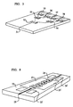
- FIG. 3 illustrates the layout of a plate that routes one optical input to one of eight outputs and thereby encompasses an entire combiner coupler.
- an optical signal is injected in entry port 31.
- the signal enters the first level switch (32) which directs the signal to either one of two outputs.
- This switch "a splitter” because diagrammatically it looks like it splits the incoming path into two outgoing paths.
- Each outgoing path of the first level splitter is connected to a second level splitter.
- the second level output paths are connected to third level splitters.
- the four third level splitters (35-38) have eight output paths.
- the signal entering port 31 is injected into either splitter 33 or splitter 34; and the splitter with the signal routes it to either one of its outputs. Since the state of the splitter without the signal is completely irrelevant, the second level splitters share a common control signal. Similarly, the third level splitters share a common control signal. The optical signal of port 31 is routed in this manner to one of the eight output paths.
- the control pads that control the routing, and the signals that are applied to the control pads are not shown in FIG. 3 for sake of simplicity. It is understood, however, that an actual implementation includes the necessary controls. Since the combiner couplers arrangement is completely symmetric to the splitter couplers arrangement, in accordance with our invention the entire switch can be made up of identical plates. Simply reversing the entry point of light converts an combiner coupler into a splitter coupler.
- FIG. 4 depicts our novel arrangement for the plates of FIG. 3, which realizes the switch architecture of FIG. 2 -- an 8 ⁇ 8 optical crossbar switch.
- the plates of the splitter couplers are stacked substantially parallel to each other with the edges that contain the eight outputs being lined up with each other. The result of such stacking is that a rectangular array of output ports is formed when viewed at end-on.
- the rows of the array are formed from the collection of output ports of each horizontal plate, and the columns of the array are formed from the collection of output ports having the same relative position in each of the horizontal plates.
- the spacing between the combiner plates must be adjusted to correspond to the spacing between the output ports of the splitter plates, and vice-versa.
- FIG. 4 The arrangement of plates as shown in FIG. 4, once invented for the purpose of realizing the interconnection pattern of FIG. 2, presents no implementation problem in the electronic arts. Just as Wise interconnected his circuit boards to form a Banyan Network, so would the FIG. 4 interconnection of plates be realized. In the integrated waveguide electrooptic art, however, the interconnection is not simple because the polarization of light exiting the splitter plates must be matched, in most waveguide material technologies, to the required polarization of light that enters the combiner plates to minimize the voltages required to control the switches.
- FIG. 5 presents one solution in conformance with the principles of our invention.
- the splitters and combiners of the FIG. 4 arrangement are identical and, therefore, the crystal cut of the plates requires a particular polarization mode of the light passing through the channels.
- a rotation in the polarization plane of the light is necessary.
- the combiner and splitter couplers are separated somewhat from each other, and a half wave plate 150 is inserted therebetween.
- the polarization axis of plate 150 must be adjusted properly (at 45° with respect to the plane of the plates) and when so adjusted, the polarization of light exiting the splitter couplers is rotated by 90° prior to its injection into the combiner couplers.
- Imaging lenses can be included on either or both sides of plate 150 for more effective focusing of the light onto the combiner channels. That is, when it is deemed that the coupling loss between the splitter plates and the combiner plates is too great because of the spacing introduced by plate 150, one can separate the two stacks still further by two focal lengths of a focusing lens and insert two such lens as shown in FIG. 6.
- FIG. 6 is the front view of the stack arrangement. It should be realized, of course, that the use of half wave plate 150 requires the orientation of the combiner plates to be close to 90° away from the orientation of the splitter plates. If one wishes to employ a magnetic means for polarization rotation, a Faraday rotator can be substituted for plate 150; and with such a rotator the 90° spatial orientation would not necessarily have to be maintained.
- FIG. 2 structure is created with butt coupling of the combiner and splitter couplers, as depicted in FIG. 7.
- the combiner couplers and the splitter couplers of the FIG. 6 realization are not identical. Specifically, the combiner couplers and the splitter couplers are manufactured for different preferred light polarizations and, more specifically, for preferred light polarizations that are 90° rotated.
- the splitter plates can be manufactured, for example, for a preferred light polarization (e.g., requiring minimum control voltage) that is perpendicular to the large flat surface of the plates. The plane of polarization of the incoming signal is then arranged to be perpendicular to the large surface of the splitter plates.
- the polarization of light exiting the splitter couplers and entering the combiner couplers is consequently in a plane that is parallel to the large surface of the combiner plates.
- the different combiner and splitter plates can be created from different materials, or from the same material.
- Lithium Niobate substrates are used.
- One of the plates e.g. the combiner plates
- the other is manufactured with a z-cut crystal orientation.
- the 8 includes a light channel 25, electrodes 22 and 22′ which provide an input phase shift to the light within channel 25, electrodes 24 and 24′ which provide mode conversion, and electrodes 23 and 23′ which provide an output phase shift.
- the input phase shift electrodes change an injected light that is circularly or elliptically polarized into a linearly polarized light.
- the mode converter electrodes convert the polarized light from one mode to another, and the output phase shift electrodes insure that the light exiting the device is, again, linearly polarized.
- FIG. 9 presents the front view of a plate that includes a polarization converter at each output.
- a polarization converter at each output.
- the spatial phase shift induced by the polarization converters in both the combiner plates and the splitter plates is only 45°.
- polarization converters would not need to include the input phase shift electrodes because, in the application of FIG. 9, the input signal is of a known polarization.
- FIG. 5 illustrates the condition where the combiner plates and the splitter plates are at 90° to each other. That is neither a requirement nor a limitation of our structure. The only requirement is that the light at the output ports of the combiner plates, or splitter plates, should be efficiently coupled (i.e., with minimum loss) to the input ports of the splitter plates, or combiner plates. Since the channels of the combiner plates are situated directly across from the channels of the splitter plates, one can visualize the centers of the two sets of channels to be connected by pins about which the plates can rotate. With no spacers between plates, the structure is unstable, and can be collapsed so that the plates of each set (combiners and splitters) are touching each other. This is shown in FIG. 10, diagrams A and B.
- the B structure is a more compact and physically stable implementation, but it requires a rotation of the polarization of light through less than 90°( ⁇ ). That can be accomplished with the plates used in the embodiment of FIG. 9, but with the input phase shift electrodes included and the voltage on the phase shift electrodes adjusted to provide the desired spatial phase shift.
Landscapes
- Physics & Mathematics (AREA)
- General Physics & Mathematics (AREA)
- Engineering & Computer Science (AREA)
- Optics & Photonics (AREA)
- Theoretical Computer Science (AREA)
- Computer Networks & Wireless Communication (AREA)
- Optical Integrated Circuits (AREA)
- Optical Couplings Of Light Guides (AREA)
Claims (13)
- Optische Verbindungsanordnung umfassend
eine Vielzahl M von Ausgangsplatten, die jede einen Eingangsport (31) und N Ausgangsports haben und die jede optische Kanäle zum Führen optischer Energie von dem Eingangsport zu den Ausgangsports der jeweiligen Ausgangsplatte haben, wobei die N Ausgangsports optische Energie im wesentlichen entlang einer Linie zuführen können, wobei die Ausgangsplatten im wesentlichen parallel zueinander sind, wobei ein Feld von Ausgangsenergieports ausgebildet wird,
mit einer Vielzahl N von Eingangsplatten, die jede einen Ausgangsport und M Eingangsports haben und die jede optische Kanäle zum Führen von optischer Energie von den Eingangsports zu dem Ausgangsport der jeweiligen Eingangsplatte haben, wobei die M Eingangsports optische Energie im wesentlichen entlang einer Linie empfangen können, wobei die Eingangsplatten im wesentlichen parallel zueinander sind,
mit einer Einrichtung zum Koppeln der optischen Energie des Ausgangsports j der Ausgangsplatte i in die Vielzahl M von Ausgangsplatten zum Eingangsport i der Eingangsplatte j in der Vielzahl N von Eingangsplatten, wobei i eine ganze Zahl im Bereich von 1 bis M und j eine ganze Zahl im Bereich von 1 bis N ist, und
mit einer oder beiden der nachfolgenden Alternativen:a) einer Schalteinrichtung (32-38) innerhalb jeder der Ausgangsplatten, die auf ein erstes Steuersignal anspricht, um optische Energie vom Eingangsport (31) zu wenigstens einem der Ausgangsports der jeweiligen Ausgangsplatte selektiv zu führen und/oderb) einer Schalteinrichtung innerhalb jeder der Eingangsplatten, die auf ein zweites Steuersignal anspricht, um optische Energie von den Eingangsport zu dem Ausgangsport der jeweiligen Eingangsplatte selektiv zu führen. - Anordnung nach Anspruch 1,
bei welcher die Ausgangsplatten im wesentlichen senkrecht zu den Eingangsplatten sind. - Anordnung nach Anspruch 1,
bei welcher die Platten aus Lithiumniobat hergestellt sind. - Anordnung nach Anspruch 3,
bei welcher die Kanäle Kanäle von diffundiertem Titan im Lithiumniobat sind. - Anordnung nach Anspruch 1,
bei welcher jede Eingangsplatte und jede Ausgangsplatte eine Vielzahl elektrooptischer Wellenleitermodulatoren umfaßt. - Anordnung nach Anspruch 5,
bei welcher jede Eingangsplatte umfaßt:
eine Anzahl von Wegführungsniveaus, die gleich log₂N ist, wobei N eine Potenz von 2 ist, und gleich log₂N aufgerundet ist, wenn N keine Potenz von 2 ist,
wobei jedes Wegführungsniveau höchstens 2j-1 der Modulatoren enthält, wobei j eine ganze Zahl ist, welche das Niveau bezeichnet mit j = 1, 2, ...,
wobei jeder Modulator einen Eingang und zwei Ausgänge hat, und
der Eingang jedes Modulators in einem Niveau j > 1 mit einem Ausgang eines Modulators in einem Niveau j-1 verbunden ist. - Anordnung nach Anspruch 1, bei welcher:
jede der Eingangsplatten eine polarisationsdrehende Einrichtung umfaßt, die zwischen der Einrichtung zum Führen optischer Signale und den Ausgangsports angeordnet ist, und wobei jede Ausgangsplatte eine polarisationsdrehende Einrichtung umfaßt, die zwischen der Einrichtung zum Führen optischer Signale und den Eingangsports angeordnet ist. - Anordnung nach Anspruch 7,
bei welcher die Polarisationsdrehung, die durch eine polarisationsdrehende Einrichtung an einer der Eingangsplatten verursacht wird, sich zu der Polarisationsdrehung addiert, welche durch eine polarisationsdrehende Einrichtung an einer der Ausgangsplatten verursacht wird, um eine räumliche Drehung der Polarisation um 90° zu bewirken. - Anordnung nach Anspruch 7,
bei welcher die durch eine polarisationsdrehende Einrichtung an einer der Eingangsplatten verursachte Polarisationsdrehung sich zu der durch eine polarisationsdrehende Einrichtung an einer der Ausgangsplatten erzeugte Polarisationsdrehung zu einem Winkel α addiert, der im wesentlichen der gleiche Winkel ist, den die Eingangsplatten in Bezug auf die Ausgangsplatten haben. - Anordnung nach Anspruch 1,
bei welcher die Einrichtung zum Koppeln eine polarisationsdrehende Einrichtung (150) aufweist. - Anordnung nach Anspruch 10,
ferner umfassend eine fokussierende Linse, die an wenigstens einer Seite der polarisationsdrehenden Einrichtung angeordnet ist. - Anordnung nach Anspruch 1,
bei welcher die Ausgangsplatten aus einem Material hergestellt sind, das einen ersten bevorzugten Polarisationszustand zum Führen von Licht hat, während die Eingangsplatten aus einem Material hergestellt sind, das einen zweiten bevorzugten Polarisationszustand für das Führen von Licht hat, und wobei der erste und der zweite Polarisationszustand im wesentlichen senkrecht zueinander sind. - Anordnung nach Anspruch 12,
bei welcher die Ausgangsplatten im wesentlichen senkrecht zu den Eingangsplatten sind und die Ausgangsports der Ausgangsplatten den Eingangsport der Eingangsplatten zugewandt sind.
Applications Claiming Priority (2)
| Application Number | Priority Date | Filing Date | Title |
|---|---|---|---|
| US07/350,962 US5009477A (en) | 1989-05-12 | 1989-05-12 | Optical interconnect arrangement |
| US350962 | 1989-05-12 |
Publications (2)
| Publication Number | Publication Date |
|---|---|
| EP0457974A1 EP0457974A1 (de) | 1991-11-27 |
| EP0457974B1 true EP0457974B1 (de) | 1995-11-08 |
Family
ID=23378973
Family Applications (1)
| Application Number | Title | Priority Date | Filing Date |
|---|---|---|---|
| EP90304788A Expired - Lifetime EP0457974B1 (de) | 1989-05-12 | 1990-05-02 | Optische Koppelvorrichtung |
Country Status (6)
| Country | Link |
|---|---|
| US (1) | US5009477A (de) |
| EP (1) | EP0457974B1 (de) |
| JP (1) | JPH0321932A (de) |
| CA (1) | CA2015480C (de) |
| DE (1) | DE69023489T2 (de) |
| HK (1) | HK78396A (de) |
Families Citing this family (56)
| Publication number | Priority date | Publication date | Assignee | Title |
|---|---|---|---|---|
| US5274487A (en) * | 1989-12-29 | 1993-12-28 | Fujitsu Limited | Photonic switching system |
| GB9007139D0 (en) * | 1990-03-30 | 1990-05-30 | British Telecomm | Optical component |
| US5155785A (en) * | 1991-05-01 | 1992-10-13 | At&T Bell Laboratories | Optical fiber interconnection apparatus and method |
| NL9101532A (nl) * | 1991-09-10 | 1993-04-01 | Nederland Ptt | Golflengte-selectieve multiplexer en demultiplexer. |
| US5233453A (en) * | 1992-04-29 | 1993-08-03 | International Business Machines Corporation | Space-division switched waveguide array filter and method using same |
| US5248977A (en) * | 1992-05-26 | 1993-09-28 | Trw Inc. | One-dimensional electronic image scanner |
| US5255332A (en) * | 1992-07-16 | 1993-10-19 | Sdl, Inc. | NxN Optical crossbar switch matrix |
| US5351317A (en) * | 1992-08-14 | 1994-09-27 | Telefonaktiebolaget L M Ericsson | Interferometric tunable optical filter |
| US5373517A (en) * | 1993-02-19 | 1994-12-13 | At&T Corp. | Rapidly tunable integrated laser |
| US5373516A (en) * | 1993-02-19 | 1994-12-13 | At&T Corp. | Rapidly tunable wideband integrated laser |
| US5379358A (en) * | 1993-12-21 | 1995-01-03 | At&T Corp. | Optical switch having spatial light modulators |
| US5455878A (en) * | 1994-08-15 | 1995-10-03 | The Boeing Company | Programmable signal time delay device using electro-optic and passive waveguide circuits on planar substrates |
| CA2199848C (en) * | 1994-09-14 | 2003-11-11 | Lothar Stoll | Optical 1xn and nxn switching matrix having a tree structure |
| US5729642A (en) * | 1995-10-02 | 1998-03-17 | The Boeing Company | N×N optical switch array using electro-optic and passive waveguide circuits on planar substrates |
| US6072923A (en) * | 1996-04-30 | 2000-06-06 | Wavefront Research, Inc. | Optical switching, routing, and time delay systems using switched mirrors |
| US6473211B2 (en) | 1996-04-30 | 2002-10-29 | Agilent Technologies, Inc. | Optical crossbar switching and/or routing system |
| US6570684B1 (en) | 1996-04-30 | 2003-05-27 | Agilent Technologies, Inc. | Optical routing/switching systems |
| US6585382B1 (en) | 1996-04-30 | 2003-07-01 | Agilent Technologies, Inc. | Optical systems using switched mirrors |
| US5734764A (en) * | 1996-09-10 | 1998-03-31 | International Business Machines Corporation | Method and apparatus for achieving a fully-connected nonblocking optical crossbar switch having wide transfer paths and minimal latency by exploiting the transparency of silicon at selected wavelengths |
| US6115155A (en) | 1996-10-29 | 2000-09-05 | Chorum Technologies Inc. | System for dealing with faults in an optical link |
| US6545783B1 (en) | 1996-10-29 | 2003-04-08 | Chorum Technologies Lp | Optical wavelength add/drop multiplexer |
| US6163393A (en) | 1996-10-29 | 2000-12-19 | Chorum Technologies Inc. | Method and apparatus for wavelength multipexing/demultiplexing |
| US6847786B2 (en) | 1996-10-29 | 2005-01-25 | Ec-Optics Technology, Inc. | Compact wavelength filter using optical birefringence and reflective elements |
| US6243200B1 (en) | 2000-03-02 | 2001-06-05 | Chorum Technologies, Inc. | Optical wavelength router based on polarization interferometer |
| CA2217688C (en) | 1997-10-07 | 2006-12-05 | Gary Duck | Coupling of light into a monolithic waveguide device |
| DE19813920A1 (de) * | 1998-03-28 | 1999-09-30 | Bosch Gmbh Robert | Verfahren zum Schalten einer optischen Schaltmatrix |
| US6366713B1 (en) * | 1998-09-04 | 2002-04-02 | Tellabs Operations, Inc. | Strictly non-blocking optical switch core having optimized switching architecture based on reciprocity conditions |
| US6519060B1 (en) | 1999-06-04 | 2003-02-11 | Chorum Technologies Lp | Synchronous optical network in frequency domain |
| US7167615B1 (en) | 1999-11-05 | 2007-01-23 | Board Of Regents, The University Of Texas System | Resonant waveguide-grating filters and sensors and methods for making and using same |
| US6363182B2 (en) | 2000-07-31 | 2002-03-26 | James D. Mills | Optical switch for reciprocal traffic |
| US6850662B1 (en) | 2000-07-31 | 2005-02-01 | Tellabs Operations, Inc. | Optical switch for reciprocal traffic |
| US6493480B1 (en) * | 2000-07-31 | 2002-12-10 | Corning Incorporated | Multistage optical cross-connect |
| US6594437B1 (en) | 2000-08-15 | 2003-07-15 | Fci Americas Technology, Inc. | Optical fiber separation and regrouping device |
| EP1370894B1 (de) * | 2001-01-17 | 2013-03-13 | The Whitaker LLC | Optischer crossconnect |
| US6755573B2 (en) * | 2001-01-29 | 2004-06-29 | Martin Hoffmann | Full mesh optical interconnect |
| KR100389533B1 (ko) * | 2001-04-13 | 2003-06-27 | 금호엔지니어링 (주) | 지하 매설물 공동 덕트 구조체 |
| JP3885602B2 (ja) * | 2001-04-23 | 2007-02-21 | オムロン株式会社 | 光学素子及び当該光学素子を用いた光トランシーバその他の光学装置 |
| CN100376909C (zh) * | 2001-04-23 | 2008-03-26 | 欧姆龙株式会社 | 光学元件、使用该光学元件的光收发器及其他光学装置 |
| US7061944B2 (en) | 2001-05-25 | 2006-06-13 | International Business Machines Corporation | Apparatus and method for wavelength-locked loops for systems and applications employing electromagnetic signals |
| US6751014B2 (en) | 2001-06-19 | 2004-06-15 | International Business Machines Corporation | Automatic gain control and dynamic equalization of erbium doped optical amplifiers in wavelength multiplexing networks |
| US6515786B1 (en) | 2001-08-03 | 2003-02-04 | Chorum Technologies Lp | Bandwidth variable wavelength router and method of operation |
| US7062166B2 (en) | 2001-09-26 | 2006-06-13 | International Business Machines Corporation | First and second derivative processing of wavelength multiplexed optical signals |
| US6970649B2 (en) * | 2001-10-30 | 2005-11-29 | International Business Machines Corporation | WDMA free space broadcast technique for optical backplanes and interplanar communications |
| FR2832812B1 (fr) * | 2001-11-29 | 2004-01-23 | Commissariat Energie Atomique | Dispositif de multiplexage d'une matrice de canaux optiques, application au multiplexage en longueur d'onde et a l'insertion-extraction |
| US6819821B2 (en) * | 2002-03-26 | 2004-11-16 | Agilent Technologies, Inc. | Optical switch with a geometry based on perpendicularly-oriented planar lightwave circuit switches |
| US6859574B2 (en) * | 2002-04-03 | 2005-02-22 | Lucent Technologies Inc. | N×N switching arrangement of two planar arrays without waveguide crossings |
| AU2003278712A1 (en) * | 2002-08-13 | 2004-02-25 | The Regents Of The University Of California | Compact wavelength-selective optical crossconnect |
| JP4789460B2 (ja) * | 2004-12-22 | 2011-10-12 | 株式会社アドバンテスト | 光スイッチ及び光試験装置 |
| JP4704125B2 (ja) * | 2005-06-22 | 2011-06-15 | 浜松ホトニクス株式会社 | 光デバイス |
| CN101821673A (zh) * | 2007-08-14 | 2010-09-01 | 塞莱斯系统集成公司 | 电力驱动光移频器 |
| US20100124391A1 (en) * | 2008-11-18 | 2010-05-20 | Mark David Feuer | Growable multi-degree ROADM |
| WO2013111562A1 (ja) * | 2012-01-23 | 2013-08-01 | 日本電気株式会社 | 光回路、調心システムおよび光回路の調心方法 |
| US12468093B2 (en) * | 2020-09-16 | 2025-11-11 | Sumitomo Electric Industries, Ltd. | Optical wiring and optical connection method |
| JP2022184729A (ja) * | 2021-05-31 | 2022-12-13 | Tdk株式会社 | 集積光源モジュール |
| JP2024113981A (ja) * | 2023-02-10 | 2024-08-23 | 富士通オプティカルコンポーネンツ株式会社 | 光デバイス、光モジュール及び光トランシーバ |
| DE102024131556A1 (de) | 2024-10-29 | 2026-04-30 | Q.ant GmbH | Baugruppe mit zumindest zwei sequentiell angeordneten photonisch integrierten Schaltungen oder Stapeln von photonisch integrierten Schaltungen |
Family Cites Families (6)
| Publication number | Priority date | Publication date | Assignee | Title |
|---|---|---|---|---|
| US3872293A (en) * | 1972-01-07 | 1975-03-18 | Us Navy | Multi-dimensional fourier transform optical processor |
| US4384760A (en) * | 1980-12-15 | 1983-05-24 | Bell Telephone Laboratories, Incorporated | Polarization transformer |
| DE3218193C2 (de) * | 1982-05-14 | 1985-05-15 | ANT Nachrichtentechnik GmbH, 7150 Backnang | Opto-elektronische Schaltmatrix |
| FR2547150A1 (fr) * | 1983-05-31 | 1984-12-07 | Cit Alcatel | Commutateur opto-mecanique et ensemble de commutation spatiale le mettant en application |
| DE3517785A1 (de) * | 1985-05-17 | 1986-11-20 | Philips Patentverwaltung Gmbh, 2000 Hamburg | Vorrichtung zum drehen der polarisationsebene linear polarisierten lichtes und verfahren zu deren herstellung |
| US4787692A (en) * | 1987-03-13 | 1988-11-29 | American Telephone And Telegraph Company At&T Bell Laboratories | Electro optical switch architectures |
-
1989
- 1989-05-12 US US07/350,962 patent/US5009477A/en not_active Expired - Lifetime
-
1990
- 1990-04-26 CA CA002015480A patent/CA2015480C/en not_active Expired - Fee Related
- 1990-05-02 DE DE69023489T patent/DE69023489T2/de not_active Expired - Fee Related
- 1990-05-02 EP EP90304788A patent/EP0457974B1/de not_active Expired - Lifetime
- 1990-05-10 JP JP2118858A patent/JPH0321932A/ja active Pending
-
1996
- 1996-05-02 HK HK78396A patent/HK78396A/en not_active IP Right Cessation
Non-Patent Citations (3)
| Title |
|---|
| IEEE JOURNAL OF QUANTUM ELECTRONICS, vol QE-17, no 6, June 1981, pp 946-959, New York, US; R.C. ALFERNES: "Guided-Wave Devices for Optical Communication" * |
| JOURNAL OF LIGHTWAVE TECHNOLOGY, vol LT-3, no 2, April 1985, pp 230-235, New York, US; A. HIMENO et al.: "4 x 4 Optical-Gate Matrix Switch" * |
| PATENT ABSTRACTS OF JAPAN, vol 11, no 19 (P-537)(2466), 20 January 1987 & JP A 61194408 * |
Also Published As
| Publication number | Publication date |
|---|---|
| US5009477A (en) | 1991-04-23 |
| CA2015480C (en) | 1994-07-26 |
| EP0457974A1 (de) | 1991-11-27 |
| HK78396A (en) | 1996-05-10 |
| DE69023489D1 (de) | 1995-12-14 |
| DE69023489T2 (de) | 1996-06-05 |
| JPH0321932A (ja) | 1991-01-30 |
| CA2015480A1 (en) | 1990-11-12 |
Similar Documents
| Publication | Publication Date | Title |
|---|---|---|
| EP0457974B1 (de) | Optische Koppelvorrichtung | |
| Alferness | Waveguide electrooptic switch arrays | |
| Spanke | Architectures for large nonblocking optical space switches | |
| Hinton | An introduction to photonic switching fabrics | |
| US5946116A (en) | 1 X N digitally programmable optical routing switch | |
| US6452702B1 (en) | N×M digitally programmable optical routing switch | |
| US5606439A (en) | Tunable add/drop optical filter | |
| EP0349597B1 (de) | Verbesserungen in elektro-optischen schalterarchitekturen | |
| JP3842511B2 (ja) | 多重ポート・カプラを使用する光学的空間スイッチ | |
| US5162944A (en) | Optical space switch and network for such optical space switches | |
| CN1230313A (zh) | 容错的光路由选择开关 | |
| US4932735A (en) | Integrated optical hybrid matrix switches with very low crosstalk | |
| Granestrand et al. | Pigtailed tree-structured 8/spl times/8 LiNbO/sub 3/switch matrix with 112 digital optical switches | |
| CA2380577A1 (en) | Dense tree optical switch network | |
| CA1320370C (en) | Optical crossover network | |
| Granestrand et al. | Strictly nonblocking 8× 8 integratedoptic switch matrix in Ti: LiNbO3 | |
| US6839472B1 (en) | Solid state optical interconnect system | |
| Noguchi et al. | Rearrangeable multichannel free-space optical switch using polarisation multiplexing technique | |
| Yamaguchi et al. | Analog free-space optical switch structure based on cascaded beam shifters | |
| JPH0513289B2 (de) | ||
| Ailawadi | Photonic switching architectures and their comparison | |
| Yamaguchi et al. | Recent free-space photonic switches | |
| Ito et al. | A polarization-switched optically reconfigurable interconnection network | |
| Granestrand et al. | Polarization independent 4× 4 switch matrix in LiNbO3 for communicative and distributive switching | |
| Himeno et al. | Recent progress on silica-based optical switches and free-space optical switches |
Legal Events
| Date | Code | Title | Description |
|---|---|---|---|
| PUAI | Public reference made under article 153(3) epc to a published international application that has entered the european phase |
Free format text: ORIGINAL CODE: 0009012 |
|
| AK | Designated contracting states |
Kind code of ref document: A1 Designated state(s): DE GB |
|
| 17P | Request for examination filed |
Effective date: 19920521 |
|
| 17Q | First examination report despatched |
Effective date: 19940202 |
|
| RAP3 | Party data changed (applicant data changed or rights of an application transferred) |
Owner name: AT&T CORP. |
|
| GRAA | (expected) grant |
Free format text: ORIGINAL CODE: 0009210 |
|
| AK | Designated contracting states |
Kind code of ref document: B1 Designated state(s): DE GB |
|
| REF | Corresponds to: |
Ref document number: 69023489 Country of ref document: DE Date of ref document: 19951214 |
|
| PLBE | No opposition filed within time limit |
Free format text: ORIGINAL CODE: 0009261 |
|
| STAA | Information on the status of an ep patent application or granted ep patent |
Free format text: STATUS: NO OPPOSITION FILED WITHIN TIME LIMIT |
|
| 26N | No opposition filed | ||
| PGFP | Annual fee paid to national office [announced via postgrant information from national office to epo] |
Ref country code: GB Payment date: 20010426 Year of fee payment: 12 |
|
| PGFP | Annual fee paid to national office [announced via postgrant information from national office to epo] |
Ref country code: DE Payment date: 20010629 Year of fee payment: 12 |
|
| REG | Reference to a national code |
Ref country code: GB Ref legal event code: IF02 |
|
| PG25 | Lapsed in a contracting state [announced via postgrant information from national office to epo] |
Ref country code: GB Free format text: LAPSE BECAUSE OF NON-PAYMENT OF DUE FEES Effective date: 20020502 |
|
| PG25 | Lapsed in a contracting state [announced via postgrant information from national office to epo] |
Ref country code: DE Free format text: LAPSE BECAUSE OF NON-PAYMENT OF DUE FEES Effective date: 20021203 |
|
| GBPC | Gb: european patent ceased through non-payment of renewal fee |
Effective date: 20020502 |