EP0458213A2 - Control circuit for controlling an operation mode in a pseudo-static RAM - Google Patents
Control circuit for controlling an operation mode in a pseudo-static RAM Download PDFInfo
- Publication number
- EP0458213A2 EP0458213A2 EP91108048A EP91108048A EP0458213A2 EP 0458213 A2 EP0458213 A2 EP 0458213A2 EP 91108048 A EP91108048 A EP 91108048A EP 91108048 A EP91108048 A EP 91108048A EP 0458213 A2 EP0458213 A2 EP 0458213A2
- Authority
- EP
- European Patent Office
- Prior art keywords
- signal
- control
- control circuit
- circuit
- control signal
- Prior art date
- Legal status (The legal status is an assumption and is not a legal conclusion. Google has not performed a legal analysis and makes no representation as to the accuracy of the status listed.)
- Granted
Links
Images


Classifications
-
- G—PHYSICS
- G11—INFORMATION STORAGE
- G11C—STATIC STORES
- G11C11/00—Digital stores characterised by the use of particular electric or magnetic storage elements; Storage elements therefor
- G11C11/21—Digital stores characterised by the use of particular electric or magnetic storage elements; Storage elements therefor using electric elements
- G11C11/34—Digital stores characterised by the use of particular electric or magnetic storage elements; Storage elements therefor using electric elements using semiconductor devices
- G11C11/40—Digital stores characterised by the use of particular electric or magnetic storage elements; Storage elements therefor using electric elements using semiconductor devices using transistors
- G11C11/401—Digital stores characterised by the use of particular electric or magnetic storage elements; Storage elements therefor using electric elements using semiconductor devices using transistors forming cells needing refreshing or charge regeneration, i.e. dynamic cells
- G11C11/406—Management or control of the refreshing or charge-regeneration cycles
- G11C11/40615—Internal triggering or timing of refresh, e.g. hidden refresh, self refresh, pseudo-SRAMs
-
- G—PHYSICS
- G11—INFORMATION STORAGE
- G11C—STATIC STORES
- G11C11/00—Digital stores characterised by the use of particular electric or magnetic storage elements; Storage elements therefor
- G11C11/21—Digital stores characterised by the use of particular electric or magnetic storage elements; Storage elements therefor using electric elements
- G11C11/34—Digital stores characterised by the use of particular electric or magnetic storage elements; Storage elements therefor using electric elements using semiconductor devices
- G11C11/40—Digital stores characterised by the use of particular electric or magnetic storage elements; Storage elements therefor using electric elements using semiconductor devices using transistors
- G11C11/401—Digital stores characterised by the use of particular electric or magnetic storage elements; Storage elements therefor using electric elements using semiconductor devices using transistors forming cells needing refreshing or charge regeneration, i.e. dynamic cells
- G11C11/4063—Auxiliary circuits, e.g. for addressing, decoding, driving, writing, sensing or timing
- G11C11/407—Auxiliary circuits, e.g. for addressing, decoding, driving, writing, sensing or timing for memory cells of the field-effect type
- G11C11/4076—Timing circuits
-
- G—PHYSICS
- G11—INFORMATION STORAGE
- G11C—STATIC STORES
- G11C7/00—Arrangements for writing information into, or reading information out from, a digital store
- G11C7/22—Read-write [R-W] timing or clocking circuits; Read-write [R-W] control signal generators or management
Definitions
- a control circuit associated with the CS standby mode in PSRAM is so arranged as will be set out below. That is, a chip enable control circuit generates a control signal group ( ⁇ CE , ⁇ P1, ⁇ P2) in synchronism with a chip enable signal CE , a chip select control circuit latches a chip select signal CS with the use of the control signal group ( ⁇ CE , ⁇ P1, ⁇ P2) and delivers a latched signal ⁇ CS as an output signal, and a write enable control circuit delivers a write enable signal WE in accordance with the latched signal ⁇ CS.
- a chip enable control circuit generates a control signal group ( ⁇ CE , ⁇ P1, ⁇ P2) in synchronism with a chip enable signal CE
- a chip select control circuit latches a chip select signal CS with the use of the control signal group ( ⁇ CE , ⁇ P1, ⁇ P2) and delivers a latched signal ⁇ CS as an output signal
- a write enable control circuit
- a relation of the operation of these control circuits to their associated signals is as follows: At a time of normal data write-in operation, a write enable signal ⁇ WE of the write enable control circuit is made active and the write series circuit is set in an operable state. With the chip enable signal CE at a "H" level, a normal standby state is involved. With the chip enable signal CE and chip select signal CS both at the "L" levels, the CS standby mode is involved. In a normal standby state and CS standby mode, the write enable signal ⁇ WE is so controlled by the write enable control circuit as to be made not active. At this time, a dissipation current is suppressed to a minimum in the write series circuit.
- a control circuit for controlling an operation mode in a pseudostatic RAM characterized by: a first control circuit for receiving a chip enable signal and generating a first control signal group in synchronism with a level variation of the chip enable signal; a second control circuit for receiving a chip select signal and first control signal group, latching the chip select signal on the basis of the first control signal group and generating a second control signal in accordance with the latched signal; and a third control circuit for receiving a write enable signal and a second control signal and predetermined one of first control signals in the first control signal group, controlling the write enable signal in accordance with the second control signal and predetermined first control signal, and generating a third control signal for data write-in control.
- Fig. 2 is a circuit diagram showing a practical arrangement of the chip enable control circuit 11 in the present embodiment.
- the chip enable signal CE is sequentially inverted through inverters 21 and 22 to provide the aforementioned control signal ⁇ CE .
- the output of the inverter 21 is supplied to one input terminal of a NAND gate 25 sequentially through inverters 23 and 24 and directly to the other input terminal of the NAND gate 25.
- the output of the NAND gate 25 is inverted by an inverter 26 to obtain the aforementioned control signal ⁇ P1. Further, the output of the inverter 26 is inverted sequentially through inverters 27 and 28 to obtain the aforementioned control signal ⁇ P2.
- Signals of the paired input/output nodes NA, NB in the differential amplifier circuit 36 are supplied to latch sections 47 and 48 for generating latched signals ⁇ CS, ⁇ CS . This is done through N channel MOS transistors 45 and 46 whose gates are supplied with the control signal ⁇ P2 set out above.
- the latches 47 and 48 are of such a type that the latch 47 comprises two inverters 49 and 50 with the output of the inverter 50 connected to the input of the inverter 49 and the latch 48 comprises two inverters 52 and 51 with the output of the inverter 52 connected to the input of the inverter 51.
Landscapes
- Engineering & Computer Science (AREA)
- Microelectronics & Electronic Packaging (AREA)
- Computer Hardware Design (AREA)
- Dram (AREA)
- Static Random-Access Memory (AREA)
Abstract
Description
- The present invention relates to a control circuit for controlling an operation mode in a pseudo-static RAM, in particular, a chip select standby mode in a pseudo-static RAM.
- In order to increase the integration density of a static RAM, memory cells are employed as in a dynamic RAM and a counter for refreshing is formed, together with the memory cells, on a common chip as known in the art. By so doing, a pseudo-static RAM (PSRAM) is realized which operates in a manner similar to that of a static RAM.
- For PSRAM, write and read modes and CS (chip select) standby mode are known as specific modes. In PSRAM, the operation mode is determined in accordance with the level of a chip select signal CS at a time when a chip enable signal
CE of PSRAM becomes a "low (L)" level. At the time when the chip enable signalCE becomes a "L" level, for example, a normal write or a normal read mode is involved if the chip select signal CS becomes a "high (H)" level and a CS standby mode is involved, if the chip select signal CS becomes a "L" level, so that a program operation, such as the write operation in a chip, is inhibited. - A control circuit associated with the CS standby mode in PSRAM is so arranged as will be set out below. That is, a chip enable control circuit generates a control signal group (
φCE , φP1, φP2) in synchronism with a chip enable signalCE , a chip select control circuit latches a chip select signal CS with the use of the control signal group (φCE , φP1, φP2) and delivers a latched signal φCS as an output signal, and a write enable control circuit delivers a write enable signalWE in accordance with the latched signal φCS. - A relation of the operation of these control circuits to their associated signals is as follows:
At a time of normal data write-in operation, a write enable signal φWE of the write enable control circuit is made active and the write series circuit is set in an operable state. With the chip enable signalCE at a "H" level, a normal standby state is involved. With the chip enable signalCE and chip select signal CS both at the "L" levels, the CS standby mode is involved. In a normal standby state and CS standby mode, the write enable signal φWE is so controlled by the write enable control circuit as to be made not active. At this time, a dissipation current is suppressed to a minimum in the write series circuit. - As a signal for controlling the write enable control circuit, a latch signal φCS is employed which is output from the chip select control circuit. The latch signal φCS is delivered as an output signal when and only when a chip select signal CS is latched by the control signal group (
φCE , φP1, φP2) subsequent to the transmission of the control signal group (φCE , φP1, φP2) to the chip select control circuit. Thus the latch signal φCS is delivered as an output signal with a considerable delay of time. - If the chip select signal CS is in the "H" level when the chip enable signal
CE falls, a write enable signal φWE of the write enable control circuit has to be made active so as to obtain a read mode. Since, however, the write enable control circuit is controlled by only the latched signal φCS, the generation of the write enable signal is delayed, causing a marked decrease in the write operation margin. - It is accordingly the object of the present invention to provide a control circuit for controlling an active mode in a pseudostatic RAM, which can reduce dissipation current at a standby time.
- According to the present invention, there is provided a control circuit for controlling an operation mode in a pseudostatic RAM, characterized by:
a first control circuit for receiving a chip enable signal and generating a first control signal group in synchronism with a level variation of the chip enable signal;
a second control circuit for receiving a chip select signal and first control signal group, latching the chip select signal on the basis of the first control signal group and generating a second control signal in accordance with the latched signal; and
a third control circuit for receiving a write enable signal and a second control signal and predetermined one of first control signals in the first control signal group, controlling the write enable signal in accordance with the second control signal and predetermined first control signal, and generating a third control signal for data write-in control. - According to the present invention, in order to prevent a delay in a variation of the third control signal for the transmission of an external-input write enable signal, the third control signal is so formed in the control circuit that a change occurs depending upon the state of the chip enable control circuit, not solely upon the state of the chip select control circuit as in the prior art. Since the third control signal of the write enable control circuit begins to vary without need to await the output of the chip select control circuit (a cause for a delay involved), the write enable control circuit can operate without the sacrifice of a PSRAM write operation margin and this can be realized, in the CS standby mode, with less dissipation power.
- This invention can be more fully understood from the following detailed description when taken in conjunction with the accompanying drawings, in which:
- Fig. 1 is a circuit diagram showing part of an arrangement associated with a CS standby mode in a PSRAM on a first embodiment of the present invention;
- Fig. 2 is a circuit diagram showing a practical form of part of a circuit arrangement shown in Fig. 1;
- Fig. 3 is a circuit diagram showing a practical form of another part of a circuit arrangement shown in Fig. 1;
- Fig. 4 is a circuit diagram showing a practical form of still another part of a circuit arrangement shown in Fig. 1; and
- Fig. 5 is a timing chart showing respective signals showing a circuit operation of Fig. 1.
- An embodiment of the present invention will be explained below with reference to the accompanying drawings.
- Fig. 1 is a circuit diagram showing a control circuit corresponding to a section associated with a CS standby mode in a PSRAM of the present embodiment. A chip enable
control circuit 11 generates a control signal group (φCE , φP1, φP2) in synchronism with a chip enable signalCE . The chipselect control circuit 12 receives the control signal group (φCE , φP1, φP2), latches a chip select signal CS with the use of these control signals, and delivers a latched signalφCS as an output signal. A write enablecontrol circuit 13 is responsive to an inverted replica of the latched signalφCS and inverted replica of the control signal coming from thecontrol circuits WE as an internal write enable signal φWE, enabling data to be written into a memory cell, not shown. It is to be noted that the latched signalsφCS and control signalφCE are supplied as the control signals φO and φCE to the write enablecontrol circuit 13 after they have been passed throughinverters 14 and 15, respectively. - Fig. 2 is a circuit diagram showing a practical arrangement of the chip enable
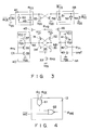
control circuit 11 in the present embodiment. The chip enable signalCE is sequentially inverted throughinverters φCE . The output of theinverter 21 is supplied to one input terminal of aNAND gate 25 sequentially throughinverters NAND gate 25. The output of theNAND gate 25 is inverted by aninverter 26 to obtain the aforementioned control signal φP1. Further, the output of theinverter 26 is inverted sequentially throughinverters - Fig. 3 is a circuit diagram showing a practical arrangement of a chip
select control circuit 12 in Fig. 1. Thecontrol circuit 12 includes a CMOS typedifferential amplifier 36 comprised of Pchannel MOS transistors channel MOS transistors channel MOS transistor 33 is of such an active type as to make the differential amplifier circuit active. The aforementioned control signal φP2 is supplied to the gate of theMOS transistor 33. - A chip select signal input section 40 comprises a P channel MOS transistor 37 and N
channel MOS transistors 38, 39 and the output of the signal input section 40 is supplied to one input/output node NA of thedifferential amplifier circuit 36. A referencevoltage input section 44 comprises a Pchannel MOS transistor 41 and N channel MOS transistors 42, 43 and the output of the referencevoltage input section 44 is supplied to the other input/output node NB. The Pchannel MOS transistors 37 and 41 of the chip select signal input section 40 and referencevoltage input section 44, respectively, are used as load transistors and a ground voltage Vss is applied to the gates of thetransistors 37 and 41. The control signal φP1 as set out above is supplied to the gates of the N channel MOS transistors 38 and 42 of the chip select signal section and referencevoltage input section 44, respectively. The chip select signal CS is supplied to the gate of the Nchannel MOS transistor 39 in the chip select signal input section 40 and a reference voltage Vref is supplied to the gate of the N channel MOS transistor 43 in the referencevoltage input section 44, noting that the reference voltage Vref is set to a level intermediate between a high logic level and a low logic level voltage. - Signals of the paired input/output nodes NA, NB in the
differential amplifier circuit 36 are supplied tolatch sections φCS . This is done through Nchannel MOS transistors latches latch 47 comprises twoinverters 49 and 50 with the output of the inverter 50 connected to the input of theinverter 49 and thelatch 48 comprises twoinverters 52 and 51 with the output of the inverter 52 connected to the input of theinverter 51. A reset N channel MOS transistor 53 is connected across the input terminal of the inverter 50 in thelatch section 47 and a ground potential Vss and a reset N channel MOS transistor 54 is connected across the input terminal of the inverter 52 in the latch section and the ground potential Vss. The control signal φCE as set out above is supplied to the gates of these N channel MOS transistors 53 and 54. An Nchannel MOS transistor 55 has its drain-to-source circuit connected across theinverter 49 in thelatch circuit 47 and the ground potential Vss and an Nchannel MOS transistor 56 has its drain-to-source circuit connected across theinverter 51 in thelatch section 48 and the ground potential Vss. Thesetransistors - Fig. 4 is a detailed arrangement of a write enable
control circuit 13 in the embodiment shown in Fig. 2. Thecontrol circuit 13 comprises aNAND gate 61 supplied with the control signals φO and φCE andNOR gate 62 supplied with an output of theNAND gate 61 and write enable signalWE . The internal write enable signalφWE is obtained as an output of theNOR gate 62. - The operation of the control circuit associated with a CS standby mode in PSRAM of the present embodiment will be explained below with reference to a timing chart shown in Fig. 5.
- With the chip enable signal CE going from a "H" level (standby state) to a "L" level, if the chip select signal CS is in the "H" level, a normal data read or a normal write operation is carried out. That is, a control signal φCE generated from the chip enable
control circuit 21 goes low for a predetermined "L" level period in synchronism with a variation from the "H" to the "L" level of the chip enable signal CE. Control signals φP1, φP2 become a "H" level for a period of time. - When the chip select control circuit 12 (see Fig. 3) receives the control signals as set out above, the N channel MOS transistor 38 in the chip select signal input section 40 and N channel MOS transistor 42 in the reference
voltage input section 44 are turned ON with the "H" level of the control signal φP1 and a voltage corresponding to the chip select signal CS and reference voltage Vref emerge on the paired input/output nodes NA and NB in thedifferential amplifier circuit 36. Thetransistor 33 in thedifferential amplifier circuit 36 is turned ON with the "H" level of the control signal φP2, placing thedifferential amplifier circuit 36 in an active state. The voltages developed on the chip select signal input section 40 and referencevoltage input section 44 compare with each other, detecting a chip select signal CS logic level. - With the control signal φP2 at the "H" level, the N
channel MOS transistors differential amplifier circuit 36 are supplied to the latchingsections latch section 47 becomes a "H" level and the latched signalφCS of thelatch section 48 becomes a "L" level. - The NOR
gate circuit 62 in the write enable control circuit 13 (see Fig. 5) receives a "L" level write enable signalWE , as well as an "L" output signal delivered from theNAND date circuit 61 which has been supplied with "H" level control signals φCE and φO, and delivers a "H" level signal as an internal write enable signal φWE. That is, a "H" level output control signal φCE is delivered from the inverter 15 (see Fig. 1) as indicated by anarrow 71 in Fig. 5 and a write enable signalWE is reversed at the NORgate 62 in the write enablecontrol circuit 13. The NORgate 62 delivers a corresponding "H" level signal as an internal write enable signal φWE. Thereafter, a write series circuit performs a data write-in control, not shown. - After a chip select signal CS has become a "L" level, a chip enable signal
CE changes to a "H" level standby mode. Then a "H" level control signalφCE is generated from the chip enablecontrol circuit 11 and the transistors 53 and 54 in the chip select control circuit 13 (see Fig. 3) are turned ON. When this occurs, thelatch sections φCS are set to "L" levels. Thus, the control signals φO and φCE are supplied to the write enablecontrol circuit 13 as shown in Fig. 1 and become a "H" and a "L" level, respectively. An output of theNAND gate circuit 61 in the write enablecontrol circuit 13 becomes a "H" level. As a result, the internal write enable signal φWE changes from the "H" level to a "L" level. Thereafter, a data write control operation is inhibited in a data write series circuit. - Then a chip enable signal
CE changes from a "H" to a "L" level at which time a CS standby mode is involved with the chip select signal CS at the "L" level. Then the control signalφCE of the chip enablecontrol circuit 11 becomes a "L" level for a predetermined period of time and the control signals φP1 and φP2 of the chip enablecontrol circuit 11 becomes a "H" level during a predetermined period of time. - When the chip
select control circuit 12 receives these control signals, an inverted replica φCE of theinverter 15 initially becomes a "H" level as indicated by anarrow 71 in Fig. 5 and the write enable signalWE is inverted in the NORgate 62 in the write enablecontrol circuit 13 and delivered as a "H" level internal write enable signalφWE from the write enablecontrol circuit 13. Since, however, the latch signal φCS of thelatch section 47 and latch signalφCS of thelatch section 48 become a "L" and "H" level, respectively, with the chip select signal CS at a "L" level, an inverted control signal φO of the latch signalφCS changes from the "H" level to a "L" level. As a result, the internal write enable signal φWE rapidly changes to a "L" level as indicated by anarrow 72 in Fig. 5 and a data write control operation is inhibited in the write series circuit, not shown. - In this way, the control signal φO supplied to the write enable
control circuit 13 is normally placed in a high potential level and becomes a low potential level only when the chip select signal CS becomes a low potential level with a fall in the chip enable signalCE . It is designed that, when the chip enable signalCE goes high, the control signal φO goes back to a high potential level. By so doing, the operation delay time of the write enable control circuit can be made shorter than in the conventional standby mode, securing no loss of the write operation margin. Since, at a time of the CS standby mode, the write enable signalWE is rapidly rendered in an non-active state, it is possible to simultaneously realize a circuit arrangement of less dissipation power. - According to the present invention, as set out above, a control circuit for controlling an operation mode in a pseudostatic RAM for reducing a dissipation current at the standby time is accomplished without a sacrifice of the write operation margin.
Claims (7)
- A control circuit for controlling an operation mode in a pseudo-static RAM, characterized by comprising:
a first control circuit (11) for receiving a chip enable signal (CE ) and generating a first control signal group (φCE , φP1, φP2) in synchronism with a level variation of said chip enable signal (CE );
a second control circuit (12) for receiving a chip select signal (CS) and said first control signal group (φCE , φP1, φP2), latching said chip select signal (CS) on the basis of said first control signal group (φCE , φP1, φP2) and generating a second control signal (φO) in accordance with the latched signal (φCS ); and
a third control circuit (13) for receiving a write enable signal (WE ) and said second control signal (φO) and predetermined one of first control signals in said first control signal group (φCE , φP1, φP2), controlling said write enable signal (WE ) in accordance with the predetermined control signal and said second control signal (φO) and generating a third control signal (φWE) for data write-in control. - The control circuit according to claim 1, characterized in that said predetermined control signal (
φCE ) in said control signal group (φCE , φP1, φP2) which is supplied to said third control circuit (13) is supplied from said first control circuit (11) to said second control circuit (12) earliest in synchronism with a variation in said chip enable signal (CE ). - The control circuit according to claim 1, characterized in that said first control circuit (11) is comprised of a pulse generation circuit for generating said first control signals (
φCE , φP1, φP2) in the first control signal group as timing signals for the operation of said second control circuit operation. - The control circuit according to claim 1, characterized in that said second control circuit (12) includes a differential amplifier for comparing said chip select signal (CS) with a reference potential (Vref) and a latch circuit (47, 48) for latching a result of detection.
- The control circuit according to claim 4, characterized in that said second control circuit (12) comprises a differential amplifier circuit for comparing said chip select signal (CS) with said reference potential (Vref) and a latch circuit (47, 48) for latching a result of detection of the differential amplifier circuit.
- The control circuit according to claim 5, characterized in that said reference potential (Vref) is set to a potential level intermediate between a high logic level and a low logic level.
- The control circuit according to claim 1, characterized in that said third control circuit (13) comprises a NAND circuit (61) for receiving said second control signal (φO) and predetermined one of first control signals in said first control signal group (
φCE , φP1, φP2) as two input signals and a NOR circuit (62) for receiving an output of said NAND circuit and write enable signal (WE) as two input signals, wherein said third control signal (φWE) is delivered as an output signal from said NOR circuit.
Applications Claiming Priority (2)
| Application Number | Priority Date | Filing Date | Title |
|---|---|---|---|
| JP2130893A JP2744115B2 (en) | 1990-05-21 | 1990-05-21 | Control circuit of pseudo static RAM |
| JP130893/90 | 1990-05-21 |
Publications (3)
| Publication Number | Publication Date |
|---|---|
| EP0458213A2 true EP0458213A2 (en) | 1991-11-27 |
| EP0458213A3 EP0458213A3 (en) | 1993-01-27 |
| EP0458213B1 EP0458213B1 (en) | 1996-01-17 |
Family
ID=15045179
Family Applications (1)
| Application Number | Title | Priority Date | Filing Date |
|---|---|---|---|
| EP91108048A Expired - Lifetime EP0458213B1 (en) | 1990-05-21 | 1991-05-17 | Control circuit for controlling an operation mode in a pseudo-static RAM |
Country Status (5)
| Country | Link |
|---|---|
| US (1) | US5301164A (en) |
| EP (1) | EP0458213B1 (en) |
| JP (1) | JP2744115B2 (en) |
| KR (1) | KR950007141B1 (en) |
| DE (1) | DE69116426T2 (en) |
Families Citing this family (9)
| Publication number | Priority date | Publication date | Assignee | Title |
|---|---|---|---|---|
| US5617551A (en) * | 1992-09-18 | 1997-04-01 | New Media Corporation | Controller for refreshing a PSRAM using individual automatic refresh cycles |
| US5590088A (en) * | 1993-07-13 | 1996-12-31 | Seiko Epson Corporation | Semiconductor memory device with enable signal conversion circuit operative for reducing current consumption |
| KR0119886B1 (en) * | 1994-07-27 | 1997-10-17 | 김광호 | Mode setting circuit of semiconductor memory device and method thereof |
| US5657293A (en) * | 1995-08-23 | 1997-08-12 | Micron Technology, Inc. | Integrated circuit memory with back end mode disable |
| KR100431303B1 (en) | 2002-06-28 | 2004-05-12 | 주식회사 하이닉스반도체 | A pseudo sram which is capable of accomplishing page write mode |
| CN1310299C (en) * | 2003-05-21 | 2007-04-11 | 中国科学院计算技术研究所 | Hazard detection and elimination method based on circuit static time-delay property |
| US6985385B2 (en) * | 2003-08-26 | 2006-01-10 | Grandis, Inc. | Magnetic memory element utilizing spin transfer switching and storing multiple bits |
| KR100695512B1 (en) | 2005-06-30 | 2007-03-15 | 주식회사 하이닉스반도체 | Semiconductor memory device |
| US10332586B1 (en) | 2017-12-19 | 2019-06-25 | Micron Technology, Inc. | Apparatuses and methods for subrow addressing |
Family Cites Families (10)
| Publication number | Priority date | Publication date | Assignee | Title |
|---|---|---|---|---|
| JPS6052513B2 (en) * | 1981-12-02 | 1985-11-19 | 富士通株式会社 | semiconductor storage device |
| US4710903A (en) * | 1986-03-31 | 1987-12-01 | Wang Laboratories, Inc. | Pseudo-static memory subsystem |
| JPH0644393B2 (en) * | 1986-04-08 | 1994-06-08 | 日本電気株式会社 | Semiconductor memory |
| JPS63166093A (en) * | 1986-12-26 | 1988-07-09 | Toshiba Corp | Control circuit for semiconductor memory |
| JP2569033B2 (en) * | 1987-01-16 | 1997-01-08 | 株式会社日立製作所 | Semiconductor storage device |
| JP2585602B2 (en) * | 1987-06-10 | 1997-02-26 | 株式会社日立製作所 | Semiconductor storage device |
| US4879683A (en) * | 1987-09-28 | 1989-11-07 | Texas Instruments Incorporated | A gaas register file having a plurality of latches |
| JPH01194194A (en) * | 1988-01-29 | 1989-08-04 | Nec Ic Microcomput Syst Ltd | Semiconductor memory device |
| JPH01205788A (en) * | 1988-02-12 | 1989-08-18 | Toshiba Corp | Semiconductor integrated circuit |
| JP2598081B2 (en) * | 1988-05-16 | 1997-04-09 | 株式会社東芝 | Semiconductor memory |
-
1990
- 1990-05-21 JP JP2130893A patent/JP2744115B2/en not_active Expired - Lifetime
-
1991
- 1991-05-17 DE DE69116426T patent/DE69116426T2/en not_active Expired - Lifetime
- 1991-05-17 EP EP91108048A patent/EP0458213B1/en not_active Expired - Lifetime
- 1991-05-17 KR KR1019910008047A patent/KR950007141B1/en not_active Expired - Fee Related
- 1991-05-20 US US07/702,375 patent/US5301164A/en not_active Expired - Lifetime
Also Published As
| Publication number | Publication date |
|---|---|
| JP2744115B2 (en) | 1998-04-28 |
| KR950007141B1 (en) | 1995-06-30 |
| EP0458213B1 (en) | 1996-01-17 |
| DE69116426D1 (en) | 1996-02-29 |
| US5301164A (en) | 1994-04-05 |
| DE69116426T2 (en) | 1996-06-05 |
| JPH0426986A (en) | 1992-01-30 |
| KR910020732A (en) | 1991-12-20 |
| EP0458213A3 (en) | 1993-01-27 |
Similar Documents
| Publication | Publication Date | Title |
|---|---|---|
| EP0017990B1 (en) | Integrated memory circuit | |
| US4417328A (en) | Random access semiconductor memory device using MOS transistors | |
| US4985868A (en) | Dynamic random access memory having improved refresh timing | |
| US4558241A (en) | Sense amplifier | |
| US4390797A (en) | Semiconductor circuit | |
| US5031147A (en) | Semiconductor memory | |
| US4104733A (en) | Address selecting circuitry for semiconductor memory device | |
| EP0176203A2 (en) | Self refresh control circuit for dynamic semiconductor memory device | |
| US3971960A (en) | Flip-flop false output rejection circuit | |
| US4733112A (en) | Sense amplifier for a semiconductor memory device | |
| US6255862B1 (en) | Latch type sense amplifier circuit | |
| JPH06132747A (en) | Semiconductor device | |
| US3938109A (en) | High speed ECL compatible MOS-Ram | |
| US4710904A (en) | Constant pulse width generator including transition detectors | |
| US5157284A (en) | Integrated circuit including an input buffer circuit having nand and nor gates | |
| EP0458213B1 (en) | Control circuit for controlling an operation mode in a pseudo-static RAM | |
| US3946369A (en) | High speed MOS RAM employing depletion loads | |
| US6292418B1 (en) | Semiconductor memory device | |
| KR910004733B1 (en) | Semiconductor memory device having data bus reset circuit | |
| US5815450A (en) | Semiconductor memory device | |
| US6798704B2 (en) | High Speed sense amplifier data-hold circuit for single-ended SRAM | |
| US4554469A (en) | Static bootstrap semiconductor drive circuit | |
| KR20000008774A (en) | AUTO-PRECHARGE APPARATUS IN A SYNCHRONOUS DRAM(Dynamic Random Access Memory) | |
| US4823322A (en) | Dynamic random access memory device having an improved timing arrangement | |
| US4571503A (en) | Supply voltage level independent clock generator |
Legal Events
| Date | Code | Title | Description |
|---|---|---|---|
| PUAI | Public reference made under article 153(3) epc to a published international application that has entered the european phase |
Free format text: ORIGINAL CODE: 0009012 |
|
| 17P | Request for examination filed |
Effective date: 19910517 |
|
| AK | Designated contracting states |
Kind code of ref document: A2 Designated state(s): DE FR GB |
|
| PUAL | Search report despatched |
Free format text: ORIGINAL CODE: 0009013 |
|
| AK | Designated contracting states |
Kind code of ref document: A3 Designated state(s): DE FR GB |
|
| 17Q | First examination report despatched |
Effective date: 19950407 |
|
| GRAA | (expected) grant |
Free format text: ORIGINAL CODE: 0009210 |
|
| AK | Designated contracting states |
Kind code of ref document: B1 Designated state(s): DE FR GB |
|
| REF | Corresponds to: |
Ref document number: 69116426 Country of ref document: DE Date of ref document: 19960229 |
|
| ET | Fr: translation filed | ||
| PLBE | No opposition filed within time limit |
Free format text: ORIGINAL CODE: 0009261 |
|
| STAA | Information on the status of an ep patent application or granted ep patent |
Free format text: STATUS: NO OPPOSITION FILED WITHIN TIME LIMIT |
|
| 26N | No opposition filed | ||
| REG | Reference to a national code |
Ref country code: GB Ref legal event code: 746 Effective date: 19981012 |
|
| REG | Reference to a national code |
Ref country code: FR Ref legal event code: D6 |
|
| REG | Reference to a national code |
Ref country code: GB Ref legal event code: IF02 |
|
| REG | Reference to a national code |
Ref country code: FR Ref legal event code: ST Effective date: 20090119 |
|
| REG | Reference to a national code |
Ref country code: FR Ref legal event code: D3 |
|
| PGFP | Annual fee paid to national office [announced via postgrant information from national office to epo] |
Ref country code: GB Payment date: 20100329 Year of fee payment: 20 |
|
| PGFP | Annual fee paid to national office [announced via postgrant information from national office to epo] |
Ref country code: FR Payment date: 20100525 Year of fee payment: 20 |
|
| PGFP | Annual fee paid to national office [announced via postgrant information from national office to epo] |
Ref country code: DE Payment date: 20100512 Year of fee payment: 20 |
|
| REG | Reference to a national code |
Ref country code: DE Ref legal event code: R071 Ref document number: 69116426 Country of ref document: DE |
|
| REG | Reference to a national code |
Ref country code: GB Ref legal event code: PE20 Expiry date: 20110516 |
|
| PG25 | Lapsed in a contracting state [announced via postgrant information from national office to epo] |
Ref country code: GB Free format text: LAPSE BECAUSE OF EXPIRATION OF PROTECTION Effective date: 20110516 |
|
| PG25 | Lapsed in a contracting state [announced via postgrant information from national office to epo] |
Ref country code: DE Free format text: LAPSE BECAUSE OF EXPIRATION OF PROTECTION Effective date: 20110517 |