EP0458611B1 - Circuit de commande de moteur - Google Patents
Circuit de commande de moteur Download PDFInfo
- Publication number
- EP0458611B1 EP0458611B1 EP91304623A EP91304623A EP0458611B1 EP 0458611 B1 EP0458611 B1 EP 0458611B1 EP 91304623 A EP91304623 A EP 91304623A EP 91304623 A EP91304623 A EP 91304623A EP 0458611 B1 EP0458611 B1 EP 0458611B1
- Authority
- EP
- European Patent Office
- Prior art keywords
- overdrive
- signals
- motor
- signal
- exciting
- Prior art date
- Legal status (The legal status is an assumption and is not a legal conclusion. Google has not performed a legal analysis and makes no representation as to the accuracy of the status listed.)
- Expired - Lifetime
Links
- 238000004804 winding Methods 0.000 claims description 35
- 238000000034 method Methods 0.000 claims description 14
- 238000013021 overheating Methods 0.000 claims description 9
- 230000001276 controlling effect Effects 0.000 description 14
- 101100464779 Saccharomyces cerevisiae (strain ATCC 204508 / S288c) CNA1 gene Proteins 0.000 description 9
- 238000010586 diagram Methods 0.000 description 5
- 101150110971 CIN7 gene Proteins 0.000 description 4
- 101150110298 INV1 gene Proteins 0.000 description 4
- 102100029469 WD repeat and HMG-box DNA-binding protein 1 Human genes 0.000 description 4
- 101710097421 WD repeat and HMG-box DNA-binding protein 1 Proteins 0.000 description 4
- 101100397044 Xenopus laevis invs-a gene Proteins 0.000 description 4
- 101100508840 Daucus carota INV3 gene Proteins 0.000 description 3
- 101100464782 Saccharomyces cerevisiae (strain ATCC 204508 / S288c) CMP2 gene Proteins 0.000 description 3
- 239000003990 capacitor Substances 0.000 description 3
- 101100286980 Daucus carota INV2 gene Proteins 0.000 description 2
- 101100397045 Xenopus laevis invs-b gene Proteins 0.000 description 2
- 230000005284 excitation Effects 0.000 description 2
- 238000004904 shortening Methods 0.000 description 2
- 238000007796 conventional method Methods 0.000 description 1
- 230000003247 decreasing effect Effects 0.000 description 1
- 238000010438 heat treatment Methods 0.000 description 1
- 238000004519 manufacturing process Methods 0.000 description 1
- 230000001105 regulatory effect Effects 0.000 description 1
- 230000000630 rising effect Effects 0.000 description 1
Images



Classifications
-
- H—ELECTRICITY
- H02—GENERATION; CONVERSION OR DISTRIBUTION OF ELECTRIC POWER
- H02P—CONTROL OR REGULATION OF ELECTRIC MOTORS, ELECTRIC GENERATORS OR DYNAMO-ELECTRIC CONVERTERS; CONTROLLING TRANSFORMERS, REACTORS OR CHOKE COILS
- H02P8/00—Arrangements for controlling dynamo-electric motors rotating step by step
- H02P8/14—Arrangements for controlling speed or speed and torque
- H02P8/18—Shaping of pulses, e.g. to reduce torque ripple
-
- H—ELECTRICITY
- H02—GENERATION; CONVERSION OR DISTRIBUTION OF ELECTRIC POWER
- H02P—CONTROL OR REGULATION OF ELECTRIC MOTORS, ELECTRIC GENERATORS OR DYNAMO-ELECTRIC CONVERTERS; CONTROLLING TRANSFORMERS, REACTORS OR CHOKE COILS
- H02P8/00—Arrangements for controlling dynamo-electric motors rotating step by step
- H02P8/14—Arrangements for controlling speed or speed and torque
- H02P8/16—Reducing energy dissipated or supplied
Definitions
- the present invention relates to a method of controlling a stepping motor and an apparatus for controlling a stepping motor.
- a high voltage is applied to phase windings of a stepping motor so that a rise time of an exciting or driving current to be supplied to the phase windings is reduced.
- the high voltage need be changed to a low voltage or cut off when the rotor reaches a given position to prevent overheating of the stepping motor caused by the supply of overcurrent to the phase windings so that the driving current to be supplied to the phase windings need be suppressed.
- US-A-4769585 discloses a method of controlling a stepping motor comprising the steps of producing an exciting signal for exciting a predetermined phase winding, producing an overdrive signal for the predetermined phase winding and supplying a drive current to the predetermined phase winding in dependence on the exciting signal and the overdrive signal, and an apparatus for controlling a stepper motor for producing control signals that control the drive current in individual phase windings of the motor, comprising an overdrive signal generator for producing overdrive signals means for producing exciting signals for exciting the phase windings, and control means for controlling said drive current in dependence on the exciting signals and overdrive signals.
- the drive circuit comprises a pulse generator 1 for generating a chain of pulses, an overdrive signal generator 2 for generating overdrive signals upon reception of the pulses, a distributing circuit 3 for producing exciting signals, transistors 4a to 4d for receiving phase exciting signals, a transistor 4e for receiving a power voltage +E1.
- the pulse generator 1 influences a speed of revolution of the stepping motor. Change of the pulse width of the overdrive signal (b) produced by the overdrive signal generator 2 influences the intensity of the driving current.
- the driving current is excessively supplied to the phase windings, thereby heating the motor while if the power voltage +E1 is low, the driving current does not supply sufficiently to the phase windings, thereby reducing the torque.
- a chopper type constant current drive circuit may be employed, but it will cause high manufacturing cost.
- the present invention solves the problems of the conventional method of controlling a stepping motor and provides a method of controlling a stepping motor capable of eliminating generation of the overcurrent, torque reduction, increase of the cost even if the stepping motor operates at its maximum performance.
- a method characterised in that during a first stage of the supply of drive current, the overdrive signal comprises pulses having a first width and, during a second stage of the supply of drive current, the overdrive signal comprises pulses having a second width, wherein the first pulse width is less than the second pulse width and the second pulse width is such that the drive current is insufficient to produce overheating of the motor.
- an apparatus characterised in that the overdrive signal generator is configured such that, during a first stage of the supply of drive current, the overdrive signals comprise pulses having a first width and, during a second stage of the supply of drive current, the overdrive signals) comprise pulses having a second width, wherein the first pulse width is less than the second pulse width and the second pulse width is such that the drive current is insufficient to produce overheating of the motor.
- the pulse widths of the overdrive signals may be compensated in accordance with the magnitude of the power voltage applied to the windings of the stepping motor. That is, the pulse width of the overdrive signal is short if the power voltage is high while it is long if the power voltage is low.
- the pulse widths of the overdrive signals may be compensated in accordance with the speed of revolution of the stepping motor. That is, the pulse width of the overdrive signal is short if the speed of revolution is high while it is long if the speed of revolution is low.
- a drive circuit for controlling the stepping motor comprises, as illustrated in Fig. 1, a pulse generator 1 for receiving a start signal and producing a chain of pulse signals, an overdrive signal generator 2′ for receiving the pulse signal from the pulse generator 1 and producing overdrive signals, a distributing circuit 3 for receiving the pulse signal from the pulse generator 1 and producing phase exciting signals, AND gates AND1 to AND4 for receiving the overdrive signals from the overdrive signal generator 2′ at one input terminals thereof and the phase exciting signals from the distributing circuit 3 at the other input terminals thereof for carrying out the logical AND between the overdrive signals and the phase exciting signals and producing control signals (c′) to (f′) for turning on transistors 4a2 to 4d2 by way of transistors 4a3 to 4d3 for a given time and in a given sequence, transistors 4a1 to 4d1 for receiving the phase exciting signals, transistors 4a2 to 4d2 for selectively receiving a power voltage +E1 and phase windings 5a and 5b of the bipolar stepping motor.
- the power voltage +E1 is supplied to the phase winding 5a so that an exciting current is flown in the direction of i1 while when the transistors 4c1 and 4c2 are turned on the exciting current is flown to the phase winding 5a in the direction of i3.
- the exciting current is flown to the phase winding 5b in the direction of i2 while when the transistors 4d1 and 4d2 are turned on, the exciting current is flown to the phase winding 5b in the direction of i4.
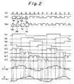
- the drive circuit for the bipolar stepping motor starts operation when the pulse generator 1 produces the pulse signal (a) upon reception of the start signal. That is, when the bipolar stepping motor is driven by one-two alternate phase exciting system, the pulse signal (a) is supplied to the distributing circuit 3 which then selectively produces phase exciting signals (c) to (f) to the transistors 4a1 to 4d1, thereby turning on the transistors 4a1 to 4d1 at a given sequence.
- the overdrive signals (b1) and (b2) are produced by the overdrive signal generator 2′ when the same generator 2′ receives the pulse signal (a) from the pulse generator 1, and go to H level so that the AND circuits AND1 to AND4 carry out the logical AND between the overdrive signals (b1) and (b2) and the phase exciting signals (c) to (f) and produce the control signals (c′) to (f′) which are supplied to the transistors 4a2 to 4d2 by way of the transistors 4a3 to 4d3.
- the transistors 4a2 to 4d2 are turned on for a given time in a given sequence, thereby supplying the power voltage +E1 to the phase windings 5a and 5b so that the forward or reverse exciting current flowing from the power voltage +E1 to the ground is supplied to the phase windings 5a and 5b.
- the overdrive signal (b1) produced by the overdrive signal generator 2′ goes to H levels at the first two pulses for a duration of t w1 and next succeeding two pulses for a duration of t w2 according to the duration where the phase exciting signals (c) and (e) go to H level.
- the control signals (c′) and (e′) produced by the AND gates AND1 and AND3 go to H levels at the first two pulses for the duration of t w1 and at succeeding one pulse for the duration of t w2 during which the transistors 4a2 and 4c2 are turned on by way of the transistors 4a3 and 4c3 and the power volatge +E1 is supplied to the phase winding 5a.
- the overdrive signal (b2) goes to H level at first two pulses for a duration of t w1 and at succeeding two pulses for a duration of t w2 in response to the duration where the phase exciting signals (d) and (f) go to H level.
- the control signals (d′) and (f′) produced by the AND gates AND2 and AND4 go to H level at first two pulses for the duration of t w1 and at a succeeding one pulse for the duration of t w2 during which the transistors 4b2 and 4d2 are turned on by way of the transistors 4b3 and 4d3 so that the power voltage +E1 is supplied to the phase winding 5b.
- the exciting or driving current is supplied to the phase winding 5a and 5b in the forward or reverse direction as illustrated in the arrows in Fig. 2 so that the stepping motor starts rotation.
- the expression of t w1 > t w2 is established between the durations t w1 and t w2 of the overdrive signals and the duration t w1 is determined so that the current is supplied sufficiently at the leading edge of the exciting current while the duration t w2 is determined so that the current does not rise sharp at the trailing edge of the exciting current, whereby the reduction of the torque caused by the overheating of the stepping motor can be prevented.
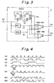
- the overdrive signal generator 2′ will be described more in detail with reference to Figs. 3 and 4.
- the overdrive signal generator 2′ comprises D-type flip-flops FF1 and FF2 serving as a mod-4 counter for counting the pulse signal (a) each time the flip-flop FF1 receives the pulse signal (a) and producing output signals (g) and (h), and one-shot multivibrators MS1 and MS2 for producing output signals (j) and (k) of H level for a duration of t w1 and a duration of t w2 each time they receive the pulse signal (a) from the pulse generator 1 and AND-OR circuits AND-OR1 and AND-OR2 for switching the output signals (j) and (k) from the one-shot multivibrators MS1 and MS2 depending on the output signal (h) from the flip-flop FF2 for producing overdrive signals (b1) and (b2).
- the overdrive signal (b1) produced by the AND-OR circuit AND-OR2 enables the one-shot multivibrator MS1 to produce the output signal (k) having the pulse width t w1 when the output signal (h) of the flip-flop FF2 goes to H level while enables the one-shot multivibrator MS2 to produce the output signal (j) having the pulse width t w2 when the output signal (h) of the flip-flop FF2 goes to L level while the overdrive signal (b2) produced by the AND-OR circuit AND-OR2 enables the one-shot multivibrator MS2 to produce the output signal (k) having the pulse width t w2 when the output signal (h) of the flip-flop FF2 goes to H level while enables the one-shot multivibrator MS1 to produce the output signal (j) having the pulse width t w1 when the output signal (h) of the flip-flop FF2 goes to L level.
- an overdrive signal (b1) and an overdrive signal (b2) are output from the overdrive signal generator 2′, the overdrive signal (b2) being shifted out of phase of 90 degrees with respect to the overdrive signal (b1) during the phase exciting period.
- phase signals (c′), (d′), (e′), (f′) acting as control signals are produced from the logic circuits AND1, AND2, AND3, AND4 by combining logically the phase exciting signals (c), (d), (e), (f) each of which is shifted by 90 degrees.
- a drive circuit for the stepping motor is substantially same as that of the first embodiment excepting that a compensating circuit is added to the overdrive signal generator of the first embodiment.
- the same and like components as those of the first embodiment are denoted at same numerals and the explanations thereof are omitted.
- a compensating circuit CMPS21 is connected to the output sides of the AND-OR circuits AND-OR1 and AND-OR2.
- the compensating circuit CMPS 21 applies a compensation pulse to the pulse widths of the output signals (b1) and (b2) of AND-OR circuits AND-OR1 and AND-OR2 depending on high or low level of the power voltage +E1. If the power voltage +E1 is high the compensation pulse width is short while the power voltage +E1 is low the compensation pulse width is long.
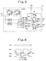
- the compensating circuit CMPS 21 comprises, as illustrated in Fig. 5, inverters INV1 and INV2 of open collectors for regulating the polarities of the output signals (b1) and (b2) of the AND-OR circuits AND-OR1 and AND-OR2, resistors R1 and R2 and capacitors C1 and C2 respectively arranged in series between the power voltage +E1 and the ground for delaying the rise time of the output signals (b11) of the inverters INV1 and INV2 depending on high or low level of the power voltage +E1.
- the compensating circuit 21 operates as follows and comparators CMP1 and CMP2 for comparing the charged capacitance voltages of the capacitors C1 and C2 with a reference voltage.
- the output signal (b11) of the inverter INV1 goes L level from the H level so that the voltage of the output signal (b11) becomes lower than a given reference voltage V th applied to a noninverting input of a comparator CMP1 so that an output signal (b1′) produced by the comparator CMP1 goes H level.
- the overdrive signal (b1) goes L level from H level
- the output of the inverter INV1 goes H level from L level. In this case, when a charged capacitance voltage of the capacitor C1 connected to the power voltage +E1 by way of the resistor R1 increases exponentially as illustrated in Fig.
- the output signal (b1′) of the comparator circuit CMP1 goes L level. That is, the compensation pulse t CMPL is added to the output signal (b1′) of the comparator CMP1 by provision of the comansating circuit CMPS 21 as illustrated in solid line in Fig. 6.
- the leading edge of the charged capacitance voltage applied to the output signal (b11) becomes gentle as illustrated in broken line in Fig. 6 so that the compensation pulse t CMPL , which is longer in the pulse width than the compensation pulse t CMPH , is applied to the output signal (b1′) of the comparator circuit CMP1.
- the provision of the compensating circuit CMPS 21 influences the overdrive signal (b2).
- the driving exciting current to be supplied to the phase windings of the stepping motor is controlled under appropriate suppressed value depending on the power voltage, thereby preventing the reduction of the torque caused by the overheating of the stepping motor.
- a drive circuit for the stepping motor is substantially the same as that of the second embodiment excepting that the compensating circuit further includes a third inverter INV3 connected to the noninverting inputs of the comparators CMP1 and CMP2 for switching the given reference voltage V th to be applied to the noninverting inputs thereof depending on the speed of rotation of the stepping motor.
- the compensating circuit further includes a third inverter INV3 connected to the noninverting inputs of the comparators CMP1 and CMP2 for switching the given reference voltage V th to be applied to the noninverting inputs thereof depending on the speed of rotation of the stepping motor.
- a high-speed mode instruction signal (b3) having H level is applied from a control unit, not shown, to the inverter INV3, the reference voltage to be applied to both the comparators CMP1 and CMP2 is lowered to the value V th-H to thereby shorten the pulse width of the compensation pulse t H to be added to the output signals (b1′) and (b2′) while if the high-speed mode instruction, (b3) having low level is applied to the inverter INV3, the reference voltage is increased to the value V th-L to thereby lengthen the pulse width of the compensation pulse t L . Accordingly, it is possible to vary the compensation pulse to an appropriate value when the power voltage +E1 is supplied from the unstable power supply, thereby preventing the reduction of the torque caused by the overheating of the stepping motor.
- the overdrive signals (b1) and (b2) may be input directly to the drive circuit without using the logic circuit comprising the AND gates which receives the exciting signals.
- the overdrive signal generator is designed so as to produce an overdrive signal containing a pulse with a longer width at an earlier stage of a pulse exciting duration during which a drive current flows in a phase winding of the stepping motor and a pulse with a shorter pulse width at a later stage of said exciting duration.
- Such a circuit configuration is suited to control unipolar stepping motors.
- the pulse widths of the overdrive signals are compensated according to the level of the power voltage for driving the stepping motor. That is, when the power voltage is high, the pulse widths of the driving signals are shortened to prevent the overcurrent while the pulse widths of the driving signals are lengthened to assure the satisfactory driving current. Even if the power voltage is supplied from the unstable power supply, it is possible to maintain the driving current to be supplied to the phase windings at an appropriate value.
- the compensation pulse it is also possible to switch the compensation pulse to be added to the pulse width of the overdrive signal at least two stages depending on the speed of rotation of the stepping motor, that is, to switch the compensation pulse having short pulse width in case the speed of revolution is high and to switch the compensation pulse having long pulse width in case the speed of revolution is low. Accordingly, it is possible to regulate the compensation pulse at an appropriate value depending on the speed of revolution of the stepping motor even if the power voltage is supplied by the unstable power supply.
Landscapes
- Engineering & Computer Science (AREA)
- Power Engineering (AREA)
- Control Of Stepping Motors (AREA)
Claims (6)
- Un procédé de commande d'un moteur pas à pas comprenant les étapes qui consistent à produire un signal d'excitation (c, d, e, f) pour exciter un enroulement de phase prédéterminé (5a, 5b), à produire un signal de suralimentation (c′, d′, e′, f′) pour l'enroulement de phase prédéterminée et à appliquer un courant d'attaque à l'enroulement de phase prédéterminé (5a, 5b) sous la dépendance du signal d'excitation (c, d, e, f) et du signal de suralimentation (c′, d′, e′, f′), caractérisé en ce que, pendant un premier stade de l'application du courant d'attaque, le signal de suralimentation (c′, d′, e′, f′) est formé par des impulsions ayant une première largeur (tw1) et, pendant un second stade de l'application du courant d'attaque, le signal de suralimentation (c′, d′, e′, f′) est formé par des impulsions ayant une seconde largeur (tw2), la première largeur d'impulsion (tw1) étant inférieure à la seconde largeur d'impulsion (tw2), et la seconde largeur d'impulsion (tw2) étant telle que le courant d'attaque soit insuffisant pour produire un échauffement excessif du moteur.
- Un procédé selon la revendication 1, comprenant l'étape qui consiste à commander les largeurs d'impulsion (tw1, tw2) du signal de suralimentation sous la dépendance d'une tension d'alimentation (+E1) qui est appliquée au moteur, pour réguler le couple du moteur.
- Un procédé selon la revendication 1 ou 2, comprenant l'étape qui consiste à commander les largeurs d'impulsion (tw1, tw2) du signal d'attaque sous la dépendance de la vitesse du moteur, pour réguler le couple du moteur.
- Un dispositif pour commander un moteur pas à pas, destiné à produire des signaux de commande qui commandent le courant d'attaque dans des enroulements de phase individuels (5a, 5b) du moteur, comprenant un générateur de signaux de suralimentation (1) destiné à produire des signaux de suralimentation (c′, d′, e′, f′), des moyens (3) pour produire des signaux d'excitation (c, d, e, f′) pour exciter les enroulements de phase, et des moyens de commande (4) pour commander le courant d'attaque sous la dépendance des signaux d'excitation (c, d, e, f) et des signaux de suralimentation (c′, d′, e′, f′), caractérisé en ce que le générateur de signaux de suralimentation (1) a une configuration telle que, pendant un premier stade de l'application du courant d'attaque, les signaux de suralimentation (c′, d′, e′, f′) sont formés par des impulsions ayant une première largeur (tw1) et, pendant un second stade de l'application du courant d'attaque, les signaux de suralimentation (c′, d′, e′, f′) sont constitués par des impulsions ayant une seconde largeur (tw2), la première largeur d'impulsion (tw1) étant inférieure à la seconde largeur d'impulsion (tw2), et la seconde largeur d'impulsion (tw2) étant telle que le courant d'attaque soit insuffisant pour produire un échauffement excessif du moteur.
- Un dispositif selon la revendication 4, dans lequel les moyens de génération de signaux de suralimentation (1) réagissent à une tension d'alimentation (+E1), appliquée au moteur, en régulant le couple du moteur par la commande des largeurs d'impulsion (tw1, tw2) des signaux de suralimentation.
- Un dispositif selon la revendication 4 ou 5, dans lequel les moyens de génération de signaux de suralimentation (1) réagissent à la vitesse du moteur de façon à réguler le couple du moteur par la commande des largeurs d'impulsion (tw1, tw2) des signaux de suralimentation.
Applications Claiming Priority (2)
| Application Number | Priority Date | Filing Date | Title |
|---|---|---|---|
| JP2130390A JPH0429598A (ja) | 1990-05-22 | 1990-05-22 | ステッピングモータの駆動制御方法 |
| JP130390/90 | 1990-05-22 |
Publications (3)
| Publication Number | Publication Date |
|---|---|
| EP0458611A2 EP0458611A2 (fr) | 1991-11-27 |
| EP0458611A3 EP0458611A3 (en) | 1992-02-05 |
| EP0458611B1 true EP0458611B1 (fr) | 1994-11-30 |
Family
ID=15033174
Family Applications (1)
| Application Number | Title | Priority Date | Filing Date |
|---|---|---|---|
| EP91304623A Expired - Lifetime EP0458611B1 (fr) | 1990-05-22 | 1991-05-22 | Circuit de commande de moteur |
Country Status (4)
| Country | Link |
|---|---|
| US (1) | US5216348A (fr) |
| EP (1) | EP0458611B1 (fr) |
| JP (1) | JPH0429598A (fr) |
| DE (1) | DE69105350T2 (fr) |
Families Citing this family (7)
| Publication number | Priority date | Publication date | Assignee | Title |
|---|---|---|---|---|
| DE4232134A1 (de) * | 1992-09-25 | 1994-03-31 | Philips Patentverwaltung | Schaltungsanordnung zum Speisen eines Zweiphasen-Asynchronmotors |
| DE19519370A1 (de) * | 1995-05-26 | 1996-11-28 | Philips Patentverwaltung | Schaltungsanordnung zum Speisen eines Zweiphasen-Asynchronmotors |
| US9222618B2 (en) | 2010-11-29 | 2015-12-29 | Lincoln Industrial Corporation | Stepper motor driving a lubrication pump providing uninterrupted lubricant flow |
| US9022177B2 (en) | 2010-11-29 | 2015-05-05 | Lincoln Industrial Corporation | Pump having stepper motor and overdrive control |
| US9388940B2 (en) | 2010-11-29 | 2016-07-12 | Lincoln Industrial Corporation | Variable speed stepper motor driving a lubrication pump system |
| US9671065B2 (en) | 2013-10-17 | 2017-06-06 | Lincoln Industrial Corporation | Pump having wear and wear rate detection |
| CN108631666B (zh) * | 2017-03-15 | 2021-04-06 | 杭州三花研究院有限公司 | 一种电机控制方法及电机控制装置 |
Citations (1)
| Publication number | Priority date | Publication date | Assignee | Title |
|---|---|---|---|---|
| US4769585A (en) * | 1986-07-01 | 1988-09-06 | Oki Electric Industry Co., Ltd. | Method of controlling a line-feed stepping motor in a printer and a driver circuit therefor |
Family Cites Families (11)
| Publication number | Priority date | Publication date | Assignee | Title |
|---|---|---|---|---|
| US3972535A (en) * | 1974-11-08 | 1976-08-03 | Pertec Corporation | Spindle drive motor |
| JPS5312669A (en) * | 1976-07-21 | 1978-02-04 | Seiko Instr & Electronics Ltd | Hands reversing device of electronic watch |
| US4140955A (en) * | 1977-05-12 | 1979-02-20 | Fluke Trendar Corporation | Stepping motor drive method and apparatus |
| FR2440642A1 (fr) * | 1978-11-02 | 1980-05-30 | Gilson Med Electr | Moteur pas a pas actionne par sous-multiple du pas |
| JPS55127897A (en) * | 1979-03-26 | 1980-10-03 | Janome Sewing Mach Co Ltd | Pulse-motor-driving circuit |
| JPS589597A (ja) * | 1981-07-10 | 1983-01-19 | Fuji Xerox Co Ltd | ステツプモ−タ駆動回路 |
| JPH0767315B2 (ja) * | 1986-10-25 | 1995-07-19 | 株式会社ピーエフユー | パルス・モ−タ駆動方式 |
| US4757245A (en) * | 1987-01-08 | 1988-07-12 | Merit Machined Products | Control system for a plurality of stepper motors |
| JPS63224700A (ja) * | 1987-03-13 | 1988-09-19 | Sharp Corp | ステツプモ−タの駆動方式 |
| KR900005438B1 (ko) * | 1987-12-11 | 1990-07-30 | 삼성전자 주식회사 | 플로피 디스크 드라이브(fdd)의 스텝모터 서보제어방식 |
| JPH01291698A (ja) * | 1988-05-13 | 1989-11-24 | Sharp Corp | パルスモータ駆動回路 |
-
1990
- 1990-05-22 JP JP2130390A patent/JPH0429598A/ja active Pending
-
1991
- 1991-05-22 EP EP91304623A patent/EP0458611B1/fr not_active Expired - Lifetime
- 1991-05-22 US US07/704,057 patent/US5216348A/en not_active Expired - Lifetime
- 1991-05-22 DE DE69105350T patent/DE69105350T2/de not_active Expired - Fee Related
Patent Citations (1)
| Publication number | Priority date | Publication date | Assignee | Title |
|---|---|---|---|---|
| US4769585A (en) * | 1986-07-01 | 1988-09-06 | Oki Electric Industry Co., Ltd. | Method of controlling a line-feed stepping motor in a printer and a driver circuit therefor |
Also Published As
| Publication number | Publication date |
|---|---|
| DE69105350T2 (de) | 1995-06-22 |
| EP0458611A2 (fr) | 1991-11-27 |
| EP0458611A3 (en) | 1992-02-05 |
| DE69105350D1 (de) | 1995-01-12 |
| US5216348A (en) | 1993-06-01 |
| JPH0429598A (ja) | 1992-01-31 |
Similar Documents
| Publication | Publication Date | Title |
|---|---|---|
| US5572105A (en) | Stepping motor control method including varying the number of split sections in one step drive period of a stepping motor | |
| US4140956A (en) | Digital stepping motor drive circuit | |
| JPS6139892A (ja) | ブラシレスdcモータ駆動回路 | |
| US4463301A (en) | Step motor driving circuit | |
| JPS6111079B2 (fr) | ||
| JPH0667277B2 (ja) | ステッピングモ−タ−制御装置 | |
| JPS58154398A (ja) | ステツプモ−タの励磁回路 | |
| EP0458611B1 (fr) | Circuit de commande de moteur | |
| JPS62230396A (ja) | ステツピングモ−タ駆動回路 | |
| EP0304704B1 (fr) | Méthode et dispositif pour la commande d'un moteur pas à pas par plusieurs tensions | |
| US4506207A (en) | Step motor driving circuit | |
| US4795953A (en) | Method of and electronic circuit for starting a reluctance motor and reluctance motor provided with such an electronic circuit | |
| JPS62118794A (ja) | モ−タ駆動制御装置 | |
| US4803414A (en) | Method of controlling a step motor | |
| JP3368105B2 (ja) | ステッピングモータ制御装置及びステッピングモータ制御方法 | |
| JPH03103096A (ja) | ステッピングモータの駆動制御方法 | |
| JP2933326B2 (ja) | ステッピングモータ駆動回路 | |
| JPS6258898A (ja) | ステツピングモ−タ駆動回路 | |
| JPS58130798A (ja) | ステツプモ−タ駆動回路 | |
| JPH0421151B2 (fr) | ||
| JPH0515194A (ja) | モータ制御方法及び装置 | |
| JPH05122979A (ja) | モータのための回転速度制御回路 | |
| SU1198728A1 (ru) | Многодвигательный электропривод | |
| JPH05260798A (ja) | ステッピングモータトルク制御回路 | |
| KR940003721Y1 (ko) | 스텝모터 구동전류 제어회로 |
Legal Events
| Date | Code | Title | Description |
|---|---|---|---|
| PUAI | Public reference made under article 153(3) epc to a published international application that has entered the european phase |
Free format text: ORIGINAL CODE: 0009012 |
|
| AK | Designated contracting states |
Kind code of ref document: A2 Designated state(s): DE FR GB |
|
| PUAL | Search report despatched |
Free format text: ORIGINAL CODE: 0009013 |
|
| AK | Designated contracting states |
Kind code of ref document: A3 Designated state(s): DE FR GB |
|
| 17P | Request for examination filed |
Effective date: 19920310 |
|
| 17Q | First examination report despatched |
Effective date: 19931210 |
|
| GRAA | (expected) grant |
Free format text: ORIGINAL CODE: 0009210 |
|
| AK | Designated contracting states |
Kind code of ref document: B1 Designated state(s): DE FR GB |
|
| REF | Corresponds to: |
Ref document number: 69105350 Country of ref document: DE Date of ref document: 19950112 |
|
| ET | Fr: translation filed | ||
| PLBE | No opposition filed within time limit |
Free format text: ORIGINAL CODE: 0009261 |
|
| STAA | Information on the status of an ep patent application or granted ep patent |
Free format text: STATUS: NO OPPOSITION FILED WITHIN TIME LIMIT |
|
| 26N | No opposition filed | ||
| REG | Reference to a national code |
Ref country code: GB Ref legal event code: IF02 |
|
| PGFP | Annual fee paid to national office [announced via postgrant information from national office to epo] |
Ref country code: FR Payment date: 20060515 Year of fee payment: 16 |
|
| PGFP | Annual fee paid to national office [announced via postgrant information from national office to epo] |
Ref country code: GB Payment date: 20060517 Year of fee payment: 16 |
|
| PGFP | Annual fee paid to national office [announced via postgrant information from national office to epo] |
Ref country code: DE Payment date: 20060518 Year of fee payment: 16 |
|
| GBPC | Gb: european patent ceased through non-payment of renewal fee |
Effective date: 20070522 |
|
| REG | Reference to a national code |
Ref country code: FR Ref legal event code: ST Effective date: 20080131 |
|
| PG25 | Lapsed in a contracting state [announced via postgrant information from national office to epo] |
Ref country code: DE Free format text: LAPSE BECAUSE OF NON-PAYMENT OF DUE FEES Effective date: 20071201 |
|
| PG25 | Lapsed in a contracting state [announced via postgrant information from national office to epo] |
Ref country code: GB Free format text: LAPSE BECAUSE OF NON-PAYMENT OF DUE FEES Effective date: 20070522 |
|
| PG25 | Lapsed in a contracting state [announced via postgrant information from national office to epo] |
Ref country code: FR Free format text: LAPSE BECAUSE OF NON-PAYMENT OF DUE FEES Effective date: 20070531 |