EP0459469A1 - Méthode de gravure sèche pour semiconducteur - Google Patents
Méthode de gravure sèche pour semiconducteur Download PDFInfo
- Publication number
- EP0459469A1 EP0459469A1 EP91108833A EP91108833A EP0459469A1 EP 0459469 A1 EP0459469 A1 EP 0459469A1 EP 91108833 A EP91108833 A EP 91108833A EP 91108833 A EP91108833 A EP 91108833A EP 0459469 A1 EP0459469 A1 EP 0459469A1
- Authority
- EP
- European Patent Office
- Prior art keywords
- layer
- plasma
- gas
- etching
- semiconductor
- Prior art date
- Legal status (The legal status is an assumption and is not a legal conclusion. Google has not performed a legal analysis and makes no representation as to the accuracy of the status listed.)
- Granted
Links
Images









Classifications
-
- H—ELECTRICITY
- H10—SEMICONDUCTOR DEVICES; ELECTRIC SOLID-STATE DEVICES NOT OTHERWISE PROVIDED FOR
- H10H—INORGANIC LIGHT-EMITTING SEMICONDUCTOR DEVICES HAVING POTENTIAL BARRIERS
- H10H20/00—Individual inorganic light-emitting semiconductor devices having potential barriers, e.g. light-emitting diodes [LED]
- H10H20/80—Constructional details
- H10H20/81—Bodies
- H10H20/822—Materials of the light-emitting regions
- H10H20/824—Materials of the light-emitting regions comprising only Group III-V materials, e.g. GaP
- H10H20/825—Materials of the light-emitting regions comprising only Group III-V materials, e.g. GaP containing nitrogen, e.g. GaN
-
- H—ELECTRICITY
- H10—SEMICONDUCTOR DEVICES; ELECTRIC SOLID-STATE DEVICES NOT OTHERWISE PROVIDED FOR
- H10D—INORGANIC ELECTRIC SEMICONDUCTOR DEVICES
- H10D64/00—Electrodes of devices having potential barriers
- H10D64/01—Manufacture or treatment
- H10D64/011—Manufacture or treatment of electrodes ohmically coupled to a semiconductor
- H10D64/0116—Manufacture or treatment of electrodes ohmically coupled to a semiconductor to Group III-V semiconductors
-
- H—ELECTRICITY
- H10—SEMICONDUCTOR DEVICES; ELECTRIC SOLID-STATE DEVICES NOT OTHERWISE PROVIDED FOR
- H10H—INORGANIC LIGHT-EMITTING SEMICONDUCTOR DEVICES HAVING POTENTIAL BARRIERS
- H10H20/00—Individual inorganic light-emitting semiconductor devices having potential barriers, e.g. light-emitting diodes [LED]
- H10H20/01—Manufacture or treatment
- H10H20/011—Manufacture or treatment of bodies, e.g. forming semiconductor layers
- H10H20/013—Manufacture or treatment of bodies, e.g. forming semiconductor layers having light-emitting regions comprising only Group III-V materials
- H10H20/0133—Manufacture or treatment of bodies, e.g. forming semiconductor layers having light-emitting regions comprising only Group III-V materials with a substrate not being Group III-V materials
- H10H20/01335—Manufacture or treatment of bodies, e.g. forming semiconductor layers having light-emitting regions comprising only Group III-V materials with a substrate not being Group III-V materials the light-emitting regions comprising nitride materials
-
- H—ELECTRICITY
- H10—SEMICONDUCTOR DEVICES; ELECTRIC SOLID-STATE DEVICES NOT OTHERWISE PROVIDED FOR
- H10P—GENERIC PROCESSES OR APPARATUS FOR THE MANUFACTURE OR TREATMENT OF DEVICES COVERED BY CLASS H10
- H10P50/00—Etching of wafers, substrates or parts of devices
- H10P50/20—Dry etching; Plasma etching; Reactive-ion etching
- H10P50/24—Dry etching; Plasma etching; Reactive-ion etching of semiconductor materials
- H10P50/246—Dry etching; Plasma etching; Reactive-ion etching of semiconductor materials of Group III-V materials
-
- H—ELECTRICITY
- H10—SEMICONDUCTOR DEVICES; ELECTRIC SOLID-STATE DEVICES NOT OTHERWISE PROVIDED FOR
- H10P—GENERIC PROCESSES OR APPARATUS FOR THE MANUFACTURE OR TREATMENT OF DEVICES COVERED BY CLASS H10
- H10P50/00—Etching of wafers, substrates or parts of devices
- H10P50/69—Etching of wafers, substrates or parts of devices using masks for semiconductor materials
- H10P50/691—Etching of wafers, substrates or parts of devices using masks for semiconductor materials for Group V materials or Group III-V materials
- H10P50/692—Etching of wafers, substrates or parts of devices using masks for semiconductor materials for Group V materials or Group III-V materials characterised by their composition, e.g. multilayer masks or materials
Definitions
- the present invention relates to a dry etching method for an Al x Ga 1-x N(0 ⁇ x ⁇ 1) semiconductor.
- the Al x Ga 1-x N(0 ⁇ x ⁇ 1) semiconductor has been watched with keen interest as a material for a light emitting diode emitting a blue light and a light emitting device emitting a light with a short wavelength, and in manufacturing such a device, it is required to establish etching techniques such as mesa etching, recess etching and the like likewise the case of other compound semiconductors.
- the Al x Ga 1-x N semiconductor is a substance which is very stable chemically, and is insoluble in an acid such as hydrochloric acid, sulfuric acid, or hydrofluoric acid or a mixture thereof which is used normally as an etching fluid for other III-V group compound semiconductors. For this reason, a wet etching method using such fluids can not be applied to etching for the Al x Ga 1-x N semiconductor.
- the present inventors developed a dry etching method for the Al x Ga 1-x N(0 ⁇ x ⁇ 1) semiconductor with the plasma gas of carbon tetrachloride (CCl4) or dichlorodifluoromethane (CCl2F2). (See Japanese Laid-Open Patent Publication Nos. 278025/1989 and 278026/1989, and U.S.P. No. 4,946,548.)
- the carbon tetrachloride (CCl4) and the dichlorodifluoromethane (CCl2F2) are designated as the substances destroying the ozone layer and are to be completely forbidden to be used by A.D. 2000. Also, the problem is reported that since polymers comprising carbon are formed on the etched surface of the semiconductor in the plasma etching with the gas comprising carbon, the etched surface is lowered in quality.
- Predicting a gas having a desirable reaction characteristic in the plasma etching is impossible because the reaction mechanism is affected by the combination and the crystalline structure of atoms of a compound semiconductor to be etched. Accordingly, prediction cannot be made on whether or not an existing reaction gas is effective for etching the Al x Ga 1-x N semiconductor.
- an object of the present invention is to provide a dry etching method for the Al x Ga 1-x N semiconductor.
- Another object of the present invention is to facilitate manufacture of a light emitting diode emitting a blue light by establishing the dry etching method for the Al x Ga 1-x N semiconductor.
- a further object of the present invention is to make a precise ohmic contact on an etched surface.
- the present inventors have zealously carried out experimental studies on the etching rate, the kind of reaction gases to be used and other conditions in plasma etching of the Al x Ga 1-x N semiconductor, and have found the following facts as a result.
- Boron trichloride (BCl3) is the most suitable etching gas in the plasma etching for the Al x Ga 1-x N semiconductor. No crystal defect is produced in the semiconductor by the plasma etching. And also, a precise ohmic contact can be formed on an etched surface without sintering by successively etching the etched surface of Al x Ga 1-x N with the plasma of an inert gas after etching Al x Ga 1-x N with the plasma of the boron trichloride (BCl3) gas.
- BCl3 boron trichloride
- a method comprising the steps of: introducing a boron trichloride (BCl3) etching gas into a reaction chamber under vacuum; applying high-frequency power to produce the plasma of the boron trichloride (BCl3) gas; and etching the Al x Ga 1-x N (0 ⁇ x ⁇ 1) semiconductor with the plasma.
- BCl3 boron trichloride
- the flow rate of the etching gas is preferably 2-30 cc/min.
- the degree of vacuum is preferably 0.02-0.2 Torr and the high-frequency power density is preferably 0.1-0.5 W/cm2.
- a method further comprising the steps of: introducing an inert gas into the reaction chamber under vacuum after etching with the plasma of a BCl3 gas; applying high-frequency power to produce the plasma of the inert gas; and successively etching an etched surface of the Al x Ga 1-x N (0 ⁇ x ⁇ 1) semiconductor with the plasma of the inert gas after etching the Al x Ga 1-x N (0 ⁇ x ⁇ 1) semiconductor with the plasma of the boron trichloride (BCl3) gas.
- the flow rate of the inert gas is preferably 2-30 cc/min.
- the degree of vacuum is preferably 0.02-0.2 Torr
- the high-frequency power density is preferably 0.1-0.5 W/cm2
- the inert gas is preferably Ar, He, Ne, Kr, Xe, or Rn
- the etching time is preferably 2-15 minutes.
- a method further comprising the step of: forming an electrode on the surface of the Al x Ga 1-x N (0 ⁇ x ⁇ 1) semiconductor etched by the plasma of the inert gas.
- the electrode is preferably of aluminum.
- a light emitting diode comprising: a substrate; an n-layer of n-type gallium nitride compound semiconductor (Al x Ga 1-x N; 0 ⁇ x ⁇ 1); an i-layer of insulating gallium nitride compound semiconductor (Al x Ga 1-x N; 0 ⁇ x ⁇ 1) doped with p-type impurities; an electrode formed on an etched surface of the n-layer through a through hole; the through hole being formed through the i-layer to the n-layer by etching with the plasma of a boron trichloride (BCl3) gas and the through hole being successively etched by the plasma of inert gas; and an electrode formed on the surface of the i-layer.
- a boron trichloride (BCl3) gas boron trichloride
- the above-mentioned plasma etching is performed normally by employing: a parallel-electrode-type apparatus wherein electrodes whereto high-frequency power is applied are disposed in parallel and objects to be etched are disposed on the electrode; a cylindrical-electrode-type apparatus wherein electrodes whereto high-frequency power is applied are disposed cylindrically and objects to be etched are disposed in parallel to the cross-section of the cylinder; or an apparatus of other configuration. Also, the plasma state of a boron trichloride (BCl3) gas is generated by applying high-frequency power between the electrodes in the above-mentioned parallel-electrode-type apparatus or cylindrical-electrode-type apparatus.
- BCl3 boron trichloride
- FIG. 1 is a configuration view showing an apparatus for realizing an etching method of one specific embodiment in accordance with the present invention.
- FIG. 2 is a cross-sectional view showing a configuration of a sample to be etched.
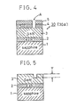
- FIG. 3 and FIG. 4 are cross-sectional views showing a relationship between the sample to be etched and a mask.
- FIG. 5 is a cross-sectional view of the sample after etching.
- FIG. 6 is a graph showing measured values of etching rate.
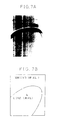
- FIG. 7A is a microphotograph showing the morphology of a surface etched by plasma of a BCl3 gas.
- FIG. 7B is an illustration indicating etched and nonetched regions in FIG. 7A.
- FIG. 8A is a microphotograph showing the morphology of a surface etched by plasma of a CCl2F2 gas.
- FIG. 8B is an illustration indicating etched and nonetched regions in FIG. 8A.
- FIG. 9A is a microphotograph showing the morphology of a surface etched by plasma of a CCl2F2 gas.
- FIG. 9B is an illustration indicating etched and nonetched regions in FIG. 9A.
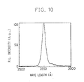
- FIG. 10 is a graph showing a photoluminescence spectrum of GaN before etching.
- FIG. 11 is a graph showing a photo luminescence spectrum of GaN after etching with plasma of a boron trichloride (BCl3) gas.
- FIG. 12 to FIG. 14 are sectional views illustrating processes for producing electrodes using a dry etching method according to another embodiment.
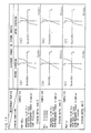
- FIG. 15 is a graph showing measured V-I characteristics of electrodes formed on various etched surfaces.
- FIG. 16 is a graph showing measured V-I characteristics of electrodes formed on nonetched surfaces of the samples used in measurements of FIG. 15.
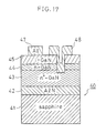
- FIG. 17 is a sectional view illustrating a light emitting diode according to another preferred embodiment of the present invention.
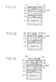
- FIGs. 18 to 24 are sectional views illustrating processes for producing a light emitting diode shown in FIG. 17.
- MOVPE metalorganic vapor phase epitaxy method
- Gases used in this method are NH3 and carrier gas H2 and trimethylgallium (Ga(CH3)3)(hereinafter referred to as “TMG”) and trimethylaluminum (Al(CH3)3) (hereinafter referred to as “TMA”).
- Ga(CH3)3) trimethylgallium
- Al(CH3)3 trimethylaluminum
- a single crystal sapphire substrate 1 whose main plane is the c-surface ( ⁇ 0001 ⁇ ) cleaned by organic cleaning and heat treatment was attached to a susceptor placed in a reaction chamber of a MOVPE apparatus.
- the pressure in the reaction chamber was reduced to 5 Torr, and the sapphire substrate 1 was vapor-etched at a temperature of 1100 °C with a H2 gas flowing into the reaction chamber at a flow rate of 300 cc/min.
- the temperature was reduced to 400 °C, and heat treatment was executed while H2 was supplied at a flow rate of 3000 cc/min., NH3 at a flow rate of 2000 cc/min., and TMA at a flow rate of 7 x 10 ⁇ 6 mol/min.
- An AlN buffer layer 2 was formed in the thickness of about 500 ⁇ by this heat treatment.
- the supply of TMA was stopped, and the temperature of the sapphire substrate 1 was kept at 1150 °C, and H2 was supplied at a rate of 2500 cc/min., NH3 at a rate of 1500 cc/min. and TMG at a rate of 1.7 x 10 ⁇ 5 mol/min., and thereby a GaN layer 3 of about 3 ⁇ m in film thickness was formed.
- a SiO2 layer 4 of 5000 ⁇ in thickness was formed on the top surface of the GaN layer 3 by high-frequency sputtering as shown in FIG. 3.
- a photoresist 5 was uniformly spreaded on the SiO2 layer 4 and a window portion A was removed from the photoresist 5 by photolithography.
- the portion of the SiO2 layer 4 which was not covered with the photoresist 5 was removed by etching with an acid of hydrofluoric acid group. Thereby, a double mask layer consisting of the SiO2 layer 4 and the photoresist 5 was formed with the window A corresponding to the etched portion of the GaN layer 3.
- the sample 30 as shown in FIG. 4 was placed in a plasma etching apparatus with parallel flat plate electrodes as shown in FIG. 1 in order to etch the exposed portion of the GaN layer 3.
- an introducing tube 12 introducing an etching gas is installed on the side wall of a stainless steel vacuum vessel 10 forming a reaction chamber 20, and the introducing tube 12 is connected to a tank 16 storing a boron trichloride (BCl3) gas through a mass flow controller 14 capable of varying the gas flow rate. Then, a BCl3 gas is introduced into the reaction chamber 20 from the tank 16 through the mass flow controller 14.
- a BCl3 gas is introduced into the reaction chamber 20 from the tank 16 through the mass flow controller 14.
- the introducing tube 12 is connected to a tank 38 storing an argon (Ar) gas through a mass flow controller 36 capable of varying the gas flow rate. Then, an Ar gas is introduced into the reaction chamber 20 from the tank 38 through the mass flow controller 36.
- Ar argon
- reaction chamber 20 is exhausted by rotary pumps 15 and 17, a diffusion pump 19 and a mechanical booster pump 13, and the degree of vacuum of the reaction chamber 20 is adjusted by a valve 18.
- an electrode 22 and an electrode 24 which are insulated from the vacuum vessel 10 are disposed in the reaction chamber 20 with facing each other in the up-down direction. Then, the electrode 22 is grounded, and the electrode 24 is supplied with high-frequency power.
- the high-frequency power is supplied from a high-frequency power source 28 with a frequency of 13.56 MHz through a matching unit 26.
- Plasma etching was performed in the apparatus having such a configuration as follows.
- the sample 30 was put on the quartz plate 25, and thereafter a residual gas in the reaction chamber 20 was fully exhausted by the diffusion pump 19, and the degree of vacuum of the reaction chamber 20 was reduced to about 5 x 10 ⁇ 6 Torr.
- a BCl3 gas was introduced into the reaction chamber 20 from the side where the electrode 24 was equipped at a flow rate of 10 cc/min. by the mass flow controller 14, and the degree of vacuum of the reaction chamber 20 was adjusted accurately to 0.04 Torr by the valve 18.
- high-frequency power of 800 W power density 0.44 W/cm2
- glow discharge was started between the electrodes 24 and 22, and the introduced BCl3 gas was put in the plasma state, and etching of the sample 30 was started.
- the sample 30 was pulled out from the reaction chamber 20 and the SiO2 layer 4 was etched to be removed by hydrofluoric acid. As a result, the sample 30 with a structure as shown in FIG. 5 was got. The portion of the GaN layer 3 covered with the SiO2 layer 4 was not etched, and only the exposed portion of the GaN layer 3 was etched in a shape as illustrated in FIG. 5. An etching depth was measured with a step difference meter.
- the etching above mentioned was repeated at different etching time, and the etching depths produced by the etching were measured with the step difference meter, and the relationship between the etching depth and the etching time was measured.
- FIG. 6 shows the result thereof. From the result of the measurement, the etching rate was 490 ⁇ /min.
- FIG. 7A One of the SEM images whose magnification is 5000 is shown in FIG. 7A.
- the etched surface in FIG. 7A is the portion corresponding to the region W in FIG. 7B.
- the etched surface is very uniform and flat, and foreign substances are not heaped on the surface.
- FIGs. 8A and 9A Typical ones of the SEM images are shown in FIGs. 8A and 9A.
- the etched surfaces in FIGs. 8A and 9A are the portions corresponding to the regions X and Y in FIGs. 8B and 9B, respectively.
- FIG. 8A many concavities exist on the etched surface.
- polymers comprising carbon are formed on the etched surface and the etched surface is not flat on account of the polymers.
- FIGs. 10 and 11 show the result thereof.
- FIG. 10 shows a photoluminescence spectrum before etching
- FIG. 11 shows a photoluminescence spectrum after etching. No change was found in the peak intensity, the peak wavelength and the half value width in the photoluminescence spectra. It was recognized from these facts that the crystalline property of the GaN layer 3 is not changed by above-mentioned etching.
- Another sample 30A was made in the construction as shown in FIG. 4 by a method as in the example 1. After the sample 30A was disposed on the electrode 25 in the reaction chamber 20, the sample 30A was etched by the plasma of a BCl3 gas for 8 minutes as in the example 1. After the etching, the supply of a BCl3 gas and the high-frequency power was stopped and an argon (Ar) gas was introduced into the reaction chamber 20 through the introducing tube 12. The flow rate of the Ar gas was controlled at 10 cc/min. by the mass flow controller 36, and the degree of vacuum of the reaction chamber 20 was adjusted accurately to 0.04 Torr by the valve 18. Then, when high-frequency power of 800 W (power density 0.44W/cm2) was supplied, glow discharge was started between the electrodes 25 and 22, and the plasma of an Ar gas was generated.
- high-frequency power of 800 W power density 0.44W/cm2
- the surface of the sample 30A was successively etched for 5 minutes after the plasma etching with BCl3.
- the sample 30A was pulled out from the reaction chamber 20 and the SiO2 layer 4 was etched to be removed by hydrofluoric acid.
- the sample 30A with the structure as shown in FIG. 5 was got.
- the sample 30A was cleaned for 10 minutes with acetone, trichloroethylene and acetone in this sequence, respectively, and was dried by blowing of a nitrogen gas.
- the sample 30A was heated at 225°C and aluminum layer 6 were uniformly deposited on the surface of the GaN layer 3 of the sample 30 at the degree of vacuum of 3 x 10 ⁇ 6 Torr as shown in FIG. 12.
- a photoresist 7 was spreaded on the aluminum 6 and unnecessary portions of the photoresist 7, i.e., the portions for electrodes to be formed on, were removed by photolithography as shown in FIG. 13.
- the portions of the aluminum 6 which were not covered with the photoresist 7 were etched by nitric acid.
- the electrodes 71 and 72 were formed on the etched surface and nonetched surface of the sample 31A, respectively, as shown in FIG. 14.
- V-I characteristic Voltage-current characteristic of the electrode 72 formed on the etched surface was measured.
- the V-I characteristic is shown in the region (b) of FIG. 15. As is apparent from the region (b) of FIG. 15, the electrode 72 shows a precise ohmic contact, because the V-I characteristic curve is linear.
- V-I characteristic was measured with respect to the sample 31A which was sintered.
- the V-I characteristic is shown in the region (e) of FIG. 15. It is found that the V-I characteristic curve is linear.
- V-I characteristic was measured with respect to the electrode which was deposited on the etched surface.
- the V-I characteristic is shown in the region (a) of FIG. 15.
- ohmic contact is not obtained, because the V-I characteristic curve is not linear.
- the V-I characteristic of the sample 31B was measured.
- the V-I characteristic is shown in the region (d) of FIG. 15. As is apparent from the region (d) of FIG. 15, ohmic contact can not be got even after sintering, because the V-I characteristic curve is not linear.
- the other sample 31C was etched using only the plasma of an Ar gas without etching with BCl3.
- V-I characteristic of the sample was measured.
- the V-I characteristic is shown in the region (c) of FIG. 15.
- ohmic contact is not realized, because the V-I characteristic curve is not linear.
- V-I characteristic of the sample 31C was measured.
- the V-I characteristic is shown in the region (f) of FIG. 15. As is apparent from the region (f) of FIG. 15, ohmic contact can not be got even after sintering, because the V-I characteristic curve is not linear.
- the V-I characteristics of the electrode 71 formed on a nonetched surface were measured. The characteristics are shown in the regions (a), (b) and (c) of FIG. 16, respectively. As is apparent from FIG. 16, ohmic contacts are not got with respect to all of the samples 31A, 31B and 31C.
- V-I characteristics were measured with respect to the samples 31A, 31B and 31C which were sintered.
- the V-I characteristics are shown in the regions (d), (e) and (f) of FIG. 16.
- ohmic contacts are realized by sintering, because the characteristic curves are linear.
- the electrode formed on the surface successively etched by the plasma of an Ar gas after etching with the plasma of a BCl3 gas is ohmic contact without sintering.
- an energy barrier seems to be formed on the surface etched by the BCl3 plasma on account of BCl3 molecule and reaction products absorbed on the surface.
- the energy barrier seems to be removed by etching with an Ar plasma. Accordingly, all other inert gases which can remove the barrier by etching are available for getting ohmic contact.
- a light emitting diode was produced by the present dry etching method.
- the production method is described as follows.
- the dry etching method according to the present invention is applied to producing electrodes in the light emitting diode with construction in FIG. 17.
- a light emitting diode 40 which has a sapphire substrate 41 on which is formed a buffer layer 42 of 500 ⁇ thick AlN.
- a buffer layer 42 of 500 ⁇ thick AlN.
- an i-(insulating) layer 45 of 0.25 ⁇ m thick GaN doped with zinc (Zn) is formed on the n-layer 44.
- Aluminum electrodes 47 and 48 are connected to the i-layer 45 and the n+-layer 43, respectively.
- the production method for the light emitting diode with this structure is described as follows.
- This light emitting diode 40 was produced by the MOVPE in the following manner.
- the gases employed in this process are NH3, H2 (as carrier gases), trimethyl gallium (Ga(CH3)3) (TMG ), trimethyl aluminum (Al(CH3)3) (TMA ), silane (SiH4), and diethyl zinc (DEZ hereinafter).
- the sapphire substrate 41 underwent vapor phase etching at 1100 °C with H2 flowing through the reaction chamber at a flow rate of 2000 cc/min under normal pressure.
- the AlN buffer layer 42 (about 500 ⁇ thick) at 400 °C by supplying H2 at a flow rate of 20,000 cc/min, NH3 at a flow rate of 10,000 cc/min, and TMA at a flow rate of 1.8 x 10 ⁇ 5 mol/min.
- the buffer layer 42 On the buffer layer 42 was formed the n+-layer 43 of high carrier concentration (1.5 x 10¹⁸/cm3) of 2.2 ⁇ m thick GaN by supplying H2 at a flow rate of 20,000 cc/min, NH3 at a flow rate of 10,000 cc/min, TMG at a flow rate of 1.7 x 10 ⁇ 4 mol/min, and silane (diluted to 0.86 ppm with H2) at a flow rate of 200 cc/min, with the sapphire substrate 41 kept at 1150 °C.
- n+-layer 43 On the n+-layer 43 was formed the n-layer 44 of low carrier concentration (1 x 10¹⁵/cm3) of 1.5 ⁇ m thick GaN by supplying H2 at a flow rate of 20,000 cc/min, NH3 at a flow rate of 10,000 cc/min, and TMG at a flow rate of 1.7 x 10 ⁇ 4 mol/min, with the sapphire substrate 41 kept at 1150 °C.
- n-layer 44 On the n-layer 44 was formed the i-layer 45 of 0.2 ⁇ m thick GaN doped with zinc by supplying H2 at a flow rate of 20,000 cc/min, NH3 at a flow rate of 10,000 cc/min, TMG at a flow rate of 1.7 x 10 ⁇ 4 mol/min, and DEZ at a flow rate of 1.5 x 10 ⁇ 4 mol/min, with the sapphire substrate 41 kept at 1000 °C.
- the photoresist layer 53 with a predetermined pattern was formed by photolithography so as for the photoresist of the etched portion (window) to remain as shown in FIG. 19.
- a 2500 ⁇ thick Al2O3 layer 52 was formed on the SiO2 layer 51 by sputtering at a pressure of 5 x 10 ⁇ 3 Torr, a high-frequency power of 300 W and a growth rate of 26 ⁇ /min.
- the sample shown in FIG. 20 was dipped in a solvent for photoresist, e.g., acetone, to remove the portion of SiO2 layer 51 and Al2O3 layer 52 right on the photoresist 53 together with the photoresist 53. Thereby the window A was formed through the SiO2 layer 51 and Al2O3 layer 52.
- a solvent for photoresist e.g., acetone
- the exposed part (the window A) of the i-layer 45 which was not covered with the SiO2 layer 51 and Al2O3 layer 52, was etched for 40 minutes by the plasma of a BCl3 gas at a flow rate of 10 cc/min and a high-frequency electric power of 0.44 W/cm2 in a vacuum of 0.04 Torr and subsequently was etched for 5 minutes with the plasma of argon, as shown in FIG. 22.
- the dry etching with BCl3 removed not only the exposed part of the i-layer 45 but also the n-layer 44 and the upper part of the n+-layer 43 which were underneath the exposed part of the i-layer 45, as shown in Fig. 22.
- the Al2O3 layer 52 as a mask was etched together.
- the Al2O3 layer 52 and SiO2 layer 51 are thick enough to remain after the etching of GaN.
- the thin Al2O3 layer 52 may remain preventing the SiO2 layer 51 from being exposed.
- the SiO2 layer 51 remaining on the i-layer 45 was removed with hydrofluorlc acid as shown in Fig. 23. Even if the Al2O3 layer 52 remains on the SiO2 layer 51, the Al2O3 layer 52 is automatically removed together with the SiO2 layer 51 which is removed from the surface of the i-layer 45.
- the GaN layers 45, 44 and 43 resist the hydrofluoric acid in the removing process of the SiO2 layer 51 and Al2O3 layer 52.
- an Al layer 54 by vapor deposition as shown in Fig. 24.
- a photoresist layer 55 which subsequently underwent the photolithographic processing to make a pattern corresponding to a figure of the electrodes connected to the n+-layer 43 and the i-layer 45, respectively.
- Such an above-mentioned process could make a gallium nitride light-emitting diode of MIS (metal-insulator-semiconductor) structure as shown in Fig. 17.
- MIS metal-insulator-semiconductor
- the SiO2 layer 51 and Al2O3 layer 52 are formed on the photoresist layer 53 and the photoresist layer 53 is removed by a solvent in order to produce a predetermined mask pattern of the SiO2 and Al2O3 layers. Since the window A is formed by removing the photoresist layer 53, the disturbance of the window shape such as undercutting is prevented.
- the Al2O3 layer 52 In etching with the plasma of BCl3 and Ar, the Al2O3 layer 52 substantially functions as a mask, Though the growth rate of Al2O3 is nearly equal to that of SiO2, the etched speed of Al2O3 is one third times lower than that of SiO2. Accordingly, the total thickness of the double mask layer of SiO2 and Al2O3 may be one third times thinner than the layer thickness in case that a mask layer is constituted of a single layer of SiO2. As a result, the time for forming the mask can be shortened. Though the mask has to be removed after etching GaN, there is not a solvent for removing only Al2O3. Accordingly, it is hard to form the mask with only the Al2O3 layer. In the embodiment described above, however, since the SiO2 layer 51 is used as the lowest mask layer, the mask of double layer structure can be easily removed with hydrofluoric acid.
- the SiO2 layer 51 is used in order to remove the mask easily, it is possible to make the SiO2 layer 51 much thinner than the Al2O3 layer 52.
- an n-layer is of a double layer structure including an n-layer of low carrier concentration contacting with an i-layer and an n+-layer of high carrier concentration.
- the n-layer may be of a single layer structure.
- the i-layer may be of a double layer structure including an i L -layer of low impurity concentration contacting with the n-layer and an i H -layer of high impurity concentration.
- the blue light intensity of the light emitting diode increased on account of a double layer structure of the n-layer. And also the blue light intensity of the light emitting diode increased on account of a double layer structure of the i-layer.
- a dry etching method for Al x Ga 1-x N(0 ⁇ x ⁇ 1) semiconductor uses plasma of a boron trichloride (BCl3) gas.
- the etching rate of the method is 490 ⁇ /min.
- No crystal defect is produced in the etched semiconductor by the dry etching with the plasma of a BCl3 gas.
- the semiconductor is successively etched by an inert gas.
- the electrode formed on the etched surface is contacted ohmicly with the semiconductor. Ohmic contact can be obtained without sintering.
- An LED is produced by the dry etching method.
- the LED comprises a substrate, an n-layer (Al x Ga 1-x N; 0 ⁇ x ⁇ 1), an i-layer, an electrode formed on the etched surface of the n-layer through a through hole, the through hole being formed through the i-layer to the n-layer by the dry etching with the plasma of the born trichloride (BCl3) gas and being successively etched by the plasma of an inert gas, and an electrode formed on the surface of said i-layer.
- n-layer Al x Ga 1-x N; 0 ⁇ x ⁇ 1
- an i-layer an electrode formed on the etched surface of the n-layer through a through hole, the through hole being formed through the i-layer to the n-layer by the dry etching with the plasma of the born trichloride (BCl3) gas and being successively etched by the plasma of an inert gas, and an electrode formed on the surface of said i-layer.
- BCl3 born trichloride
Landscapes
- Drying Of Semiconductors (AREA)
- Led Devices (AREA)
Applications Claiming Priority (2)
| Application Number | Priority Date | Filing Date | Title |
|---|---|---|---|
| JP140740/90 | 1990-05-30 | ||
| JP14074090A JP3078821B2 (ja) | 1990-05-30 | 1990-05-30 | 半導体のドライエッチング方法 |
Publications (2)
| Publication Number | Publication Date |
|---|---|
| EP0459469A1 true EP0459469A1 (fr) | 1991-12-04 |
| EP0459469B1 EP0459469B1 (fr) | 1997-03-19 |
Family
ID=15275611
Family Applications (1)
| Application Number | Title | Priority Date | Filing Date |
|---|---|---|---|
| EP91108833A Expired - Lifetime EP0459469B1 (fr) | 1990-05-30 | 1991-05-29 | Méthode de gravure sèche pour semiconducteur |
Country Status (4)
| Country | Link |
|---|---|
| US (1) | US5205905A (fr) |
| EP (1) | EP0459469B1 (fr) |
| JP (1) | JP3078821B2 (fr) |
| DE (1) | DE69125208T2 (fr) |
Cited By (3)
| Publication number | Priority date | Publication date | Assignee | Title |
|---|---|---|---|---|
| EP0860865A1 (fr) * | 1997-02-17 | 1998-08-26 | Hewlett-Packard Company | Méthode de nettoyage d'une surface d'un substrat semiconducteur |
| EP1047120A1 (fr) * | 1999-04-22 | 2000-10-25 | Sony Corporation | Méthode de fabrication d'une électrode dans un dispositif semiconducteur |
| EP1763287A3 (fr) * | 2005-09-07 | 2007-08-22 | Kabushiki Kaisha Toyota Jidoshokki | Dispositif électroluminescent organique et méthode de fabrication |
Families Citing this family (26)
| Publication number | Priority date | Publication date | Assignee | Title |
|---|---|---|---|---|
| US6362017B1 (en) | 1990-02-28 | 2002-03-26 | Toyoda Gosei Co., Ltd. | Light-emitting semiconductor device using gallium nitride group compound |
| US6830992B1 (en) * | 1990-02-28 | 2004-12-14 | Toyoda Gosei Co., Ltd. | Method for manufacturing a gallium nitride group compound semiconductor |
| CA2037198C (fr) | 1990-02-28 | 1996-04-23 | Toyoda Gosei Co., Ltd. | Dispositif luminescent utilisant un semiconducteur du groupe nitrure de gallium |
| US5633192A (en) * | 1991-03-18 | 1997-05-27 | Boston University | Method for epitaxially growing gallium nitride layers |
| US6953703B2 (en) * | 1991-03-18 | 2005-10-11 | The Trustees Of Boston University | Method of making a semiconductor device with exposure of sapphire substrate to activated nitrogen |
| WO1992016966A1 (fr) * | 1991-03-18 | 1992-10-01 | Boston University | Procede de preparation et de dopage de couches minces de nitrure de gallium monocristallin tres isolant |
| EP1313153A3 (fr) * | 1992-07-23 | 2005-05-04 | Toyoda Gosei Co., Ltd. | Dispositif semi-conducteur émetteur de lumière comprenant un composé de nitrure de gallium |
| JP2657743B2 (ja) * | 1992-10-29 | 1997-09-24 | 豊田合成株式会社 | 窒素−3族元素化合物半導体発光素子 |
| JPH07263748A (ja) * | 1994-03-22 | 1995-10-13 | Toyoda Gosei Co Ltd | 3族窒化物半導体発光素子及びその製造方法 |
| US5838029A (en) * | 1994-08-22 | 1998-11-17 | Rohm Co., Ltd. | GaN-type light emitting device formed on a silicon substrate |
| JPH08293489A (ja) * | 1995-04-25 | 1996-11-05 | Sharp Corp | 窒化ガリウム系化合物半導体のドライエッチング方法 |
| US5915164A (en) * | 1995-12-28 | 1999-06-22 | U.S. Philips Corporation | Methods of making high voltage GaN-A1N based semiconductor devices |
| EP1014455B1 (fr) | 1997-07-25 | 2006-07-12 | Nichia Corporation | Dispositif a semi-conducteur en nitrure |
| JP3770014B2 (ja) | 1999-02-09 | 2006-04-26 | 日亜化学工業株式会社 | 窒化物半導体素子 |
| WO2000052796A1 (fr) * | 1999-03-04 | 2000-09-08 | Nichia Corporation | Element de laser semiconducteur au nitrure |
| DE19920626C2 (de) * | 1999-05-05 | 2003-01-30 | Karl Hehl | Spritzgießmaschine zur Verarbeitung von Kunststoffen |
| JP2002075965A (ja) * | 2000-08-25 | 2002-03-15 | Toyoda Gosei Co Ltd | Iii族窒化物系化合物半導体素子 |
| JP3520919B2 (ja) * | 2001-03-27 | 2004-04-19 | 士郎 酒井 | 窒化物系半導体装置の製造方法 |
| US20030077910A1 (en) * | 2001-10-22 | 2003-04-24 | Russell Westerman | Etching of thin damage sensitive layers using high frequency pulsed plasma |
| US20050040212A1 (en) * | 2003-08-23 | 2005-02-24 | Kuang-Neng Yang | Method for manufacturing nitride light-emitting device |
| US20050139838A1 (en) * | 2003-12-26 | 2005-06-30 | Matsushita Electric Industrial Co., Ltd. | Semiconductor device and method for manufacturing semiconductor device |
| JP2007173465A (ja) * | 2005-12-21 | 2007-07-05 | Rohm Co Ltd | 窒化物半導体発光素子の製造方法 |
| TWI362769B (en) * | 2008-05-09 | 2012-04-21 | Univ Nat Chiao Tung | Light emitting device and fabrication method therefor |
| US8617411B2 (en) | 2011-07-20 | 2013-12-31 | Lam Research Corporation | Methods and apparatus for atomic layer etching |
| CN109234703B (zh) * | 2018-11-27 | 2020-10-16 | 湖南顶立科技有限公司 | 一种气相沉积系统 |
| TWI680503B (zh) * | 2018-12-26 | 2019-12-21 | 杰力科技股份有限公司 | 氮化鎵高電子移動率電晶體的閘極結構的製造方法 |
Citations (3)
| Publication number | Priority date | Publication date | Assignee | Title |
|---|---|---|---|---|
| US4370195A (en) * | 1982-03-25 | 1983-01-25 | Rca Corporation | Removal of plasma etching residues |
| EP0144142A2 (fr) * | 1983-11-30 | 1985-06-12 | Kabushiki Kaisha Toshiba | Procédé de fabrication d'un laser semi-conducteur |
| EP0277597A2 (fr) * | 1987-01-31 | 1988-08-10 | Toyoda Gosei Co., Ltd. | Diode electroluminescente semiconductrice du type nitride de gallium et son procédé de fabrication |
Family Cites Families (12)
| Publication number | Priority date | Publication date | Assignee | Title |
|---|---|---|---|---|
| JPS5343480A (en) * | 1976-10-01 | 1978-04-19 | Matsushita Electric Ind Co Ltd | Etching method of gallium nitride |
| US4569718A (en) * | 1980-08-22 | 1986-02-11 | At&T Bell Laboratories | Method for plasma etching III-V semiconductors with a BCl3 -Cl2 gas |
| JPS59168677A (ja) * | 1983-03-14 | 1984-09-22 | Fujitsu Ltd | 半導体装置及びその製造方法 |
| US4617193A (en) * | 1983-06-16 | 1986-10-14 | Digital Equipment Corporation | Planar interconnect for integrated circuits |
| JPS60117631A (ja) * | 1983-11-30 | 1985-06-25 | Toshiba Corp | 化合物半導体のドライエッチング方法 |
| JPS62119196A (ja) * | 1985-11-18 | 1987-05-30 | Univ Nagoya | 化合物半導体の成長方法 |
| US4911102A (en) * | 1987-01-31 | 1990-03-27 | Toyoda Gosei Co., Ltd. | Process of vapor growth of gallium nitride and its apparatus |
| JP2654454B2 (ja) * | 1988-04-29 | 1997-09-17 | 豊田合成株式会社 | 半導体のドライエッチング方法 |
| US4946548A (en) * | 1988-04-29 | 1990-08-07 | Toyoda Gosei Co., Ltd. | Dry etching method for semiconductor |
| JP2654455B2 (ja) * | 1988-04-29 | 1997-09-17 | 豊田合成株式会社 | 半導体のドライエッチング方法 |
| US4985113A (en) * | 1989-03-10 | 1991-01-15 | Hitachi, Ltd. | Sample treating method and apparatus |
| US5034092A (en) * | 1990-10-09 | 1991-07-23 | Motorola, Inc. | Plasma etching of semiconductor substrates |
-
1990
- 1990-05-30 JP JP14074090A patent/JP3078821B2/ja not_active Expired - Fee Related
-
1991
- 1991-05-29 DE DE69125208T patent/DE69125208T2/de not_active Expired - Fee Related
- 1991-05-29 EP EP91108833A patent/EP0459469B1/fr not_active Expired - Lifetime
- 1991-05-30 US US07/708,883 patent/US5205905A/en not_active Expired - Lifetime
Patent Citations (3)
| Publication number | Priority date | Publication date | Assignee | Title |
|---|---|---|---|---|
| US4370195A (en) * | 1982-03-25 | 1983-01-25 | Rca Corporation | Removal of plasma etching residues |
| EP0144142A2 (fr) * | 1983-11-30 | 1985-06-12 | Kabushiki Kaisha Toshiba | Procédé de fabrication d'un laser semi-conducteur |
| EP0277597A2 (fr) * | 1987-01-31 | 1988-08-10 | Toyoda Gosei Co., Ltd. | Diode electroluminescente semiconductrice du type nitride de gallium et son procédé de fabrication |
Non-Patent Citations (5)
| Title |
|---|
| JOURNAL OF VACUUM SCIENCE AND TECHNOLOGY: PART B. vol. 5, no. 6, November 1987, NEW YORK US pages 1599 - 1605; A. SCHERER et al.: "Gallium arsenide and aluminium gallium arsenide reactive ion etching in boron trichloride/argon mixtures" * |
| JOURNAL OF VACUUM SCIENCE AND TECHNOLOGY: PART B. vol. 7, no. 1, January 1989, NEW YORK US pages 41 - 46; S.S. COOPERMAN et al.: "Reactive ion etching of GaAs and AlGaAs in a BCl3-Ar discharge" * |
| PATENT ABSTRACTS OF JAPAN vol. 13, no. 507 (E-845) 14 November 1989, & JP-A-01 204425 (TOYOTA CENTRAL RESEARCH AND DEV. LAB. INC.) 17 August 1989, * |
| PATENT ABSTRACTS OF JAPAN vol. 6, no. 100 (P-121) 09 June 1982, & JP-A-57 033485 (HITACHI LTD.) 23 February 1982, * |
| PATENT ABSTRACTS OF JAPAN vol. 6, no. 42 (E-98)(920) 16 March 1982, & JP-A-56 160084 (MATSUSHITA DENKI SANGYO K.K.) 09 December 1981, * |
Cited By (5)
| Publication number | Priority date | Publication date | Assignee | Title |
|---|---|---|---|---|
| EP0860865A1 (fr) * | 1997-02-17 | 1998-08-26 | Hewlett-Packard Company | Méthode de nettoyage d'une surface d'un substrat semiconducteur |
| US5919715A (en) * | 1997-02-17 | 1999-07-06 | Hewlett-Packard Company | Method for cleaning a semiconductor surface |
| EP1047120A1 (fr) * | 1999-04-22 | 2000-10-25 | Sony Corporation | Méthode de fabrication d'une électrode dans un dispositif semiconducteur |
| EP1763287A3 (fr) * | 2005-09-07 | 2007-08-22 | Kabushiki Kaisha Toyota Jidoshokki | Dispositif électroluminescent organique et méthode de fabrication |
| US7470610B2 (en) | 2005-09-07 | 2008-12-30 | Kabushiki Kaisha Toyota Jidoshokki | Method of fabricating organic electroluminescent devices |
Also Published As
| Publication number | Publication date |
|---|---|
| DE69125208T2 (de) | 1997-10-09 |
| JPH0434929A (ja) | 1992-02-05 |
| EP0459469B1 (fr) | 1997-03-19 |
| US5205905A (en) | 1993-04-27 |
| DE69125208D1 (de) | 1997-04-24 |
| JP3078821B2 (ja) | 2000-08-21 |
Similar Documents
| Publication | Publication Date | Title |
|---|---|---|
| US5205905A (en) | Dry etching method for semiconductor | |
| US6358316B1 (en) | Method for producing semiconductor device, method for producing semiconductor laser device, and method for producing quantum wire structure | |
| US5693180A (en) | Dry etching method for a gallium nitride type compound semiconductor | |
| EP0762486B1 (fr) | Gravure de cristaux de nitrure | |
| US4946548A (en) | Dry etching method for semiconductor | |
| US5789265A (en) | Method of manufacturing blue light-emitting device by using BCL3 and CL2 | |
| CN1148734A (zh) | 一种半导体光发射器件及其制作方法 | |
| KR19980080216A (ko) | 에피택셜 웨이퍼 및 이의 제조방법 | |
| EP0510858A1 (fr) | Méthode de formation selective d'une couche de TiNx par MOCVD, sur un composant semi-conductor | |
| US12198936B2 (en) | Defect free germanium oxide gap fill | |
| JP2623463B2 (ja) | 窒化ガリウム系化合物半導体の電極形成方法 | |
| KR100939673B1 (ko) | 탄화 규소층의 제조방법, 질화 갈륨 반도체 소자 및 규소기판 | |
| Aoyama et al. | Silicon surface cleaning using photoexcited fluorine gas diluted with hydrogen | |
| Aoyama et al. | Surface cleaning for Si epitaxy using photoexcited fluorine gas | |
| JP2654454B2 (ja) | 半導体のドライエッチング方法 | |
| JP3610397B2 (ja) | 3族窒化物半導体の電極形成方法 | |
| US5478437A (en) | Selective processing using a hydrocarbon and hydrogen | |
| JP2740818B2 (ja) | 窒化ガリウム系化合物半導体の表面加工方法 | |
| JPH08125222A (ja) | 3族窒化物半導体の製造方法 | |
| JP2654455B2 (ja) | 半導体のドライエッチング方法 | |
| US20070034144A1 (en) | Oxide crystal growth apparatus and fabrication method using the same | |
| JP3002205B2 (ja) | 窒化ガリウム系化合物半導体の表面加工方法 | |
| JP2706660B2 (ja) | 窒化ガリウム系化合物半導体の電極形成方法 | |
| JP3639144B2 (ja) | 半導体のドライエッチング方法 | |
| US20250294920A1 (en) | Method for forming a layer with the basis of a dielectric material on a layer with the basis of an etched iii-v material |
Legal Events
| Date | Code | Title | Description |
|---|---|---|---|
| PUAI | Public reference made under article 153(3) epc to a published international application that has entered the european phase |
Free format text: ORIGINAL CODE: 0009012 |
|
| 17P | Request for examination filed |
Effective date: 19910628 |
|
| AK | Designated contracting states |
Kind code of ref document: A1 Designated state(s): DE FR GB IT |
|
| 17Q | First examination report despatched |
Effective date: 19930107 |
|
| GRAG | Despatch of communication of intention to grant |
Free format text: ORIGINAL CODE: EPIDOS AGRA |
|
| GRAH | Despatch of communication of intention to grant a patent |
Free format text: ORIGINAL CODE: EPIDOS IGRA |
|
| GRAH | Despatch of communication of intention to grant a patent |
Free format text: ORIGINAL CODE: EPIDOS IGRA |
|
| GRAA | (expected) grant |
Free format text: ORIGINAL CODE: 0009210 |
|
| AK | Designated contracting states |
Kind code of ref document: B1 Designated state(s): DE FR GB IT |
|
| RIN1 | Information on inventor provided before grant (corrected) |
Inventor name: HASHIMOTO, MASAFUMI Inventor name: MORI, MASAKI, TOYODA GOSEI TECHNICAL CENTER Inventor name: MANABE, KATSUHIDE, TOYODA GOSEI TECHNICAL CENTER Inventor name: KOTAKI, MASAHIRO, TOYODA GOSEI TECHNICAL CENTER |
|
| REF | Corresponds to: |
Ref document number: 69125208 Country of ref document: DE Date of ref document: 19970424 |
|
| ET | Fr: translation filed | ||
| PLBE | No opposition filed within time limit |
Free format text: ORIGINAL CODE: 0009261 |
|
| STAA | Information on the status of an ep patent application or granted ep patent |
Free format text: STATUS: NO OPPOSITION FILED WITHIN TIME LIMIT |
|
| 26N | No opposition filed | ||
| REG | Reference to a national code |
Ref country code: GB Ref legal event code: IF02 |
|
| PGFP | Annual fee paid to national office [announced via postgrant information from national office to epo] |
Ref country code: FR Payment date: 20050511 Year of fee payment: 15 |
|
| PGFP | Annual fee paid to national office [announced via postgrant information from national office to epo] |
Ref country code: GB Payment date: 20050525 Year of fee payment: 15 |
|
| PGFP | Annual fee paid to national office [announced via postgrant information from national office to epo] |
Ref country code: DE Payment date: 20060525 Year of fee payment: 16 |
|
| PG25 | Lapsed in a contracting state [announced via postgrant information from national office to epo] |
Ref country code: GB Free format text: LAPSE BECAUSE OF NON-PAYMENT OF DUE FEES Effective date: 20060529 |
|
| PGFP | Annual fee paid to national office [announced via postgrant information from national office to epo] |
Ref country code: IT Payment date: 20060531 Year of fee payment: 16 |
|
| GBPC | Gb: european patent ceased through non-payment of renewal fee |
Effective date: 20060529 |
|
| REG | Reference to a national code |
Ref country code: FR Ref legal event code: ST Effective date: 20070131 |
|
| PG25 | Lapsed in a contracting state [announced via postgrant information from national office to epo] |
Ref country code: FR Free format text: LAPSE BECAUSE OF NON-PAYMENT OF DUE FEES Effective date: 20060531 Ref country code: DE Free format text: LAPSE BECAUSE OF NON-PAYMENT OF DUE FEES Effective date: 20071201 |
|
| PG25 | Lapsed in a contracting state [announced via postgrant information from national office to epo] |
Ref country code: IT Free format text: LAPSE BECAUSE OF NON-PAYMENT OF DUE FEES Effective date: 20070529 |