EP0459703B1 - Mémoire adressable par le contenu - Google Patents
Mémoire adressable par le contenu Download PDFInfo
- Publication number
- EP0459703B1 EP0459703B1 EP91304677A EP91304677A EP0459703B1 EP 0459703 B1 EP0459703 B1 EP 0459703B1 EP 91304677 A EP91304677 A EP 91304677A EP 91304677 A EP91304677 A EP 91304677A EP 0459703 B1 EP0459703 B1 EP 0459703B1
- Authority
- EP
- European Patent Office
- Prior art keywords
- array
- content addressable
- data
- input signal
- row
- Prior art date
- Legal status (The legal status is an assumption and is not a legal conclusion. Google has not performed a legal analysis and makes no representation as to the accuracy of the status listed.)
- Expired - Lifetime
Links
Images

Classifications
-
- G—PHYSICS
- G11—INFORMATION STORAGE
- G11C—STATIC STORES
- G11C15/00—Digital stores in which information comprising one or more characteristic parts is written into the store and in which information is read-out by searching for one or more of these characteristic parts, i.e. associative or content-addressed stores
-
- G—PHYSICS
- G06—COMPUTING OR CALCULATING; COUNTING
- G06F—ELECTRIC DIGITAL DATA PROCESSING
- G06F16/00—Information retrieval; Database structures therefor; File system structures therefor
- G06F16/90—Details of database functions independent of the retrieved data types
- G06F16/903—Querying
- G06F16/90335—Query processing
- G06F16/90339—Query processing by using parallel associative memories or content-addressable memories
Definitions
- the present invention relates generally to memory systems and devices, and more specifically to a content addressable memory.
- Content addressable memories are used to find matches between an input data signal and data stored in a memory.
- the traditional content addressable memories have comparison circuitry imbedded in each cell of the memory array. Such an arrangement is disclosed in Wenson Conference Record, 15 Nov 1989, San Francisco, CA, US, pp 226-227. This allows the input signal to be compared with all entries within the memory at the same time. This traditional design is very fast, in that a complete catalogue of all matching entries can be made available within approximately one memory cycle of the underlying memory array.
- comparison functions other than a direct comparison such as less than, greater than or equal to, and so forth, are to be used, the number of transistors used for each cell can easily be doubled over a standard SRAM cell. This more than doubles the layout area of the cell, resulting in a large device.
- a large content addressable memory would be useful at a system level for many applications.
- database searching, and other searching and selection applications often perform simple comparisons on a large block of data.
- these searches are performed using software by scanning through a large number of memory locations looking for a match.
- "The Art of Computer Programming, Volume 3, Sorting and Searching" Donald E. Knuth, 1973, pages 393 to 394 teaches such approach.
- a content addressable memory includes a memory array having a plurality of entries. Control circuitry is provided for sequentially presenting each entry in the array to a comparator. An input signal is also provided to the comparator. Entries matching the input signal are identified for later use. The input signal can be masked, so that only selected fields of each entry are compared to it.
- Conventional RAM technology can be used for the memory array.
- a serial memory array such as an array formed from a charge coupled device, can be used.
- a content addressable memory comprising a data storage array arranged as a matrix of rows and columns, and comprising a plurality of serial shift storage devices arranged in parallel and corresponding to the columns; and wherein said select means comprises a means for shifting data in each serial shift storage device one position, a register for storing an input signal to be compared, wherein said register has a number of data bits equal to each row of the data storage array, a comparator for comparing a row in said array with the input signal, and for generating an output signal when a match occurs, select means for sequentially presenting each row of said array to said comparator for comparison with the input signal and means for storing data indicative of any matches which occur between the input signal and any rows of said array.
- a method for accessing a memory according to contents of data stored therein comprising the steps of storing data into a data storage array arranged as a matrix of rows and columns, and comprising a plurality of serial shift storage devices arranged in parallel and corresponding to the columns; and wherein said select means comprises a means for shifting data in each serial shift storage device one position, loading an input valve into a register for storing an input signal to be compared, wherein said register has a number of data bits equal to each row of the data storage array, comparing a row in said array with the input signal, and generating an output signal when a match occurs, sequentially presenting each row of said array to said comparator for comparison with the input signal and storing data indicative of any matches which occur between the input signal and any rows of said array.
- a third aspect of the present invention there is provided a method for accessing a memory according to contents of data stored therein, comprising the steps of:
- the method further comprises the step of:
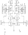
- a content addressable memory is referred to generally by reference number 10.
- a random access memory array 12 is preferably organized as a 512 entry by 1024 bit array.
- a sense amplifier 14 connected to the memory array 12 senses the data stored in a selected entry of the array 12 and presents it as output on signal line 16.
- Signal line 16 is in this example embodiment, 1024 bits wide.
- a compare register 18 is used to store an input signal value to be compared to each entry of the array 12.
- a comparator 20 compares the value stored in the compare register 18 with the value presented on signal line 16, and generates an output signal on line 22 indicating whether or not a match has occurred.
- a mask write register 24 contains a 1024 bit mask value which can be preloaded by the user. The data in the mask write register 24 determines which bits of an entry are actually compared in the comparator 20. This allows selected sub-fields of a 1024 bit entry to be used in the comparison process.
- a counter 26 is used to cycle through the values 0 - (n-1), where n is the number of routess in the memory array 12.
- the output of counter 26 is connected to a decoder 28, which in turn selects one entry within the memory array 12.
- a clock signal CLK is used to synchronize operation of the counter 26 and decoder 28.
- An alternative technique is to use a shift register for the decoder 28. This technique is similar to that used in FIFO memories, and uses a single active bit in the shift register to indicate which row is selected from the array 12. This technique provides faster access to the array 12, but is more complex to implement.
- Counter 26 also connects its output signal to select circuitry 30.
- select circuitry 30 causes the appropriate counter value to be written into a stack buffer 32.
- Stack 32 is used to retain an entry corresponding to each entry of the memory array 12 which matches the value stored in the compare register 18.
- Stack 32 may be arranged as desired, and may actually be used as a stack. It may also be organized as a queue, or it may be a register for storing a single value. In most cases, if stack 32 is actually a single register, the signal on line 22 will also cause the clock signal CLK to halt temporarily while the value stored in stack 32 is handled by other, system level, control circuitry (not shown).
- a mask value is written into the mask write register 24
- a comparison value is written into the compare register 18.
- Counter 26 is initialized to 0, and clocked 512 times in order to sequentially access each entry of the memory array 12.
- the corresponding entry number is written to the stack 32.
- the mask and compare registers 18, 24 may be written to directly from off chip. Alternatively, they may be loaded with values already in the memory array 12. By presetting the counter 26, the contents of one row are made available at the sense amplifier 14. This value can be copied directly to the mask register 24 or compare register 18 if desired. This allows one entry to be compared to the others in an efficient manner.
- Figure 2 shows an alternative design for a content addressable memory 40 which differs slightly from the content addressable memory 10 illustrated in Figure 1.
- Two memory arrays 42 each have a sense amplifier 44.
- the entries within the memory arrays 42 are compared in comparators 46 to the value stored in compare registers 48.
- Masking is performed, if desired, by data stored in mask registers 50.
- Counters 52 and decoders 54 are used to address the various entries within the arrays 42.
- Control circuitry blocks 56 controlled by outputs from the comparators 46, are used to place data into the stack buffers 58 in the same manner as described in Figure 1.
- Each array 42 is shown as having 256 entries, so that, combined, they contain the same number of entries as the memory array 12 shown in Figure 1. Since the memories are separated, however, a complete comparison can be performed in one-half the time as is required for the embodiment shown in Figure 1.
- counters 52 and decoders 54 can be combined into a single counter 52 and decoder 54, to minimize chip layout area.
- the compare registers 48 can be combined into a single compare register connected to the mask registers 50 if desired. If the layout is retained as shown in Figure 2, two comparisons can be performed. If only a single compare register 48 is used, only one value can be checked for at a time.
- Decoders 60 may also be used to access the memory arrays 42. These decoders may be connected to externally available address pins to allow direct access to be made to the memory arrays 42. This allows individual entries, or portions thereof, to be read from and written to by the external system.
- the compare register 48 and comparator 46 can be bypassed during such direct access, so that the input/output buffers are connected directly to the sense amplifiers 44.
- the data to be input to or output from the arrays 42 may pass through the compare registers 48 by correcting them directly to the sense amplifiers 44 when direct input/output to the array is to be performed.
- the decoders 54 can be designed so as to select entries within the arrays 42 based on the outputs of counters 52, and to provide direct input/output to the arrays 42 instead of using decoders 60. However, in many instances, it will be more efficient to use separate decoding circuitry 60 for the direct input/output. Decoder 54 is optimized to address data entries which are 1024 bits wide. Use of a separate decoder 60 to access the memory array 42 using data words 16 or 32 bits wide will result in higher device performance in many cases. The separate decoder 60 can also be used with the single array content addressable memory 10 described in connection with Figure 1.
- a content addressable memory generally referenced by number 70 which uses a serial access memory in place of the memory array 10.
- serial access memory can be, for example, a charge coupled device (CCD) or other serially accessed device such as a bubble memory.
- CCD charge coupled device
- a column of CCD cells 72 are connected as known in the art to form a circulating loop.
- a sense circuit 74 senses the current value in the first cell 72 of the loop, and write circuit 78 simultaneously writes a value into the last cell 72 of the loop.
- Clocking signals are provided to the loop as known in the art to shift the data in the CCD cells 72 from the last cell, where they are written, to the first cell, where they are read.
- the number of cells 72 within the loop is the number of entries within the content addressable memory 70.
- a plurality of loops, corresponding to the bit positions of the entries within the content addressable memory, are connected to the comparator 78. Thus, if a 1024 bit entry is desired, there are 1024 separate circulating loops of CCD cells 72.
- Each sense circuit 74 is connected to one bit position 80 of the comparator 78.
- the loop of CCD cells 72 is a serially accessed memory, direct access of any particular entry is not possible. Instead, it is necessary to cycle through the memory until the desired entry has reached the first cell. At this time, any desired value can be written into that entry by connecting the contents of a register (not shown) to the write circuits for each of the loops.
- CCD memories are very dense, allowing a relatively large memory to be made on a physically small device.
- analog values into CCD cells, so that multiple bits can be stored in each cell. The storage density of storing such signals in such manner must be traded off against the additional complexity and time required to decode these analog signals into their corresponding digital signals.
- Figures 1-3 illustrate a number of design tradeoffs which must be considered when fabricating content addressable memories according to the present invention.
- Figure 1 shows a device which is somewhat slower than the embodiment shown in Figure 2, but consumes less power due to the lesser number of sense amplifiers 14 and the smaller amount of control circuitry on chip. If, for example, each entry within the memory array 12 can be accessed with a cycle time of 30 nanoseconds, the total compare time for 512 routess is 15 microseconds.
- the device of Figure 2 consumes approximately twice the power of that shown in Figure 1, due to the extra sense amplifier 44. However, the same number of memory entries can be accessed in half the time. Assuming a 30 nanosecond cycle time, a 512 entry comparison can be performed in 7.5 microseconds, since only 256 comparison cycles are required.
- the device shown in Figure 3 can be made to use very low power and with high device density. It has the drawback however, that entries within the memory cannot be accessed directly for input and output as can the random access memories of Figures 1 and 2.
- memory arrays having a greater or lesser number of entries, and having different numbers of bits per entry can be made using the techniques of the present invention.
- the number of entries in the array, which determines the time needed to perform a complete comparison, and the width of each of these entries can be varied by the designer to accommodate different requirements.
- the described serial access technique allows a relatively large content addressable memory to be fabricated on a single integrated circuit chip using current technology. Although it is not as fast as a traditional content addressable memory which is accessed in parallel, it can be built much less expensively and allows for the fabrication of large memories.
- the function of the comparators in the various embodiments can be made more complex if desired.
- adding comparison functions such as less than, less than or equal to, greater than, greater than or equal to, and so forth, greatly increases the chip area required to implement the comparison function. Since only a single comparator is used for a large number of memory entries in the present technique, the comparison functions which can be applied between the memory entries and the input values can be made quite complex without adversely impacting the overall chip area required for implementation of the device. The ability to provide more complex comparison functions makes the content addressable memory more useful in some system level applications.
Landscapes
- Engineering & Computer Science (AREA)
- Databases & Information Systems (AREA)
- Theoretical Computer Science (AREA)
- Computational Linguistics (AREA)
- Data Mining & Analysis (AREA)
- Physics & Mathematics (AREA)
- General Engineering & Computer Science (AREA)
- General Physics & Mathematics (AREA)
- Dram (AREA)
- Static Random-Access Memory (AREA)
- Compression, Expansion, Code Conversion, And Decoders (AREA)
Claims (9)
- Mémoire adressable par le contenu, comprenant :un réseau de stockage de données (12, 42) organisé en une matrice de rangées et de colonnes, et comprenant plusieurs dispositifs de stockage série à décalage (72) disposés en parallèle et correspondant aux colonnes ; et dans lequel un moyen de sélection (76) comprend un moyen pour décaler d'une position les données dans chaque dispositif de stockage série à décalage ;un registre (18) pour stocker un signal d'entrée devant être comparé, dans lequel le registre (18) comprend un nombre de bits de données égal à chaque rangée du réseau de stockage de données (12, 42) ;un comparateur (20, 46) pour comparer une rangée du réseau (12, 42) au signal d'entrée, et pour produire un signal de sortie (2) lorsqu'une correspondance se produit ;des moyens de sélection (26, 28) pour présenter de manière séquentielle chaque rangée du réseau (12, 42) au comparateur pour une comparaison avec le signal d'entrée ; etun moyen (32) pour stocker des données indiquant toutes les correspondances qui se produisent entre le signal d'entrée et toutes les rangées du réseau (12, 42).
- Mémoire adressable par le contenu selon la revendication 1, dans laquelle le moyen de stockage (32) stocke, pour chaque correspondance indiquée, une valeur de compteur identifiant quelle rangée contient la correspondance.
- Mémoire adressable par le contenu selon la revendication 2, dans laquelle le moyen de stockage (32) stocke les valeurs dans une pile.
- Mémoire adressable par le contenu selon la revendication 2, dans laquelle le moyen de stockage (32) stocke les valeurs dans une file d'attente.
- Mémoire adressable par le contenu selon l'une quelconque des revendications précédentes, dans laquelle les données indiquant toutes les correspondances sont stockées dans une pile.
- Mémoire adressable par le contenu selon l'une quelconque des revendications précédentes, dans laquelle les dispositifs de stockage série à décalage (72) comprennent des dispositifs à injection de charge.
- Mémoire adressable par le contenu selon l'une quelconque des revendications 1 à 5, dans laquelle les dispositifs de stockage série à décalage (72) comprennent des dispositifs de mémoire à bulles.
- Mémoire adressable par le contenu selon l'une quelconque des revendications précédentes, qui comprend en outre :un registre de masque (24, 50) pour contenir une valeur de masque et pour sélectionner un sous-ensemble de positions de bits du signal d'entrée et de la rangée présentée qui doivent être comparés, où le signal (22) indiquant une correspondance est produit lorsqu'une correspondance se produit dans le sous-ensemble sélectionné.
- Procédé pour accéder à une mémoire en fonction des valeurs des données qui y sont stockées, qui comprend les étapes consistant à :stocker des données dans un réseau de stockage de données (12, 42) organisé en une matrice de rangées et de colonnes, et comprenant plusieurs dispositifs de stockage série à décalage (72) disposés en parallèle et correspondant aux colonnes ; et dans lequel les moyens de sélection (76) comprennent un moyen pour décaler d'une position les données dans chaque dispositif de stockage série à décalage ;charger une valeur d'entrée dans un registre (18) afin de stocker un signal d'entrée devant être comparé, où le registre (18) comporte un nombre de bits de données égal à celui de chaque rangée du réseau de stockage de données (12, 42) ;comparer une rangée du réseau (12, 42) au signal d'entrée, et produire un signal de sortie (2) lorsqu'une correspondance se produit ;présenter de manière séquentielle chaque rangée du réseau (12, 42) au comparateur pour une comparaison avec le signal d'entrée ; etstocker des données indiquant toutes les correspondances qui se produisent entre le signal d'entrée et toutes les rangées du réseau (12, 42).
Applications Claiming Priority (2)
| Application Number | Priority Date | Filing Date | Title |
|---|---|---|---|
| US53101190A | 1990-05-31 | 1990-05-31 | |
| US531011 | 1990-05-31 |
Publications (3)
| Publication Number | Publication Date |
|---|---|
| EP0459703A2 EP0459703A2 (fr) | 1991-12-04 |
| EP0459703A3 EP0459703A3 (en) | 1993-07-28 |
| EP0459703B1 true EP0459703B1 (fr) | 2000-08-16 |
Family
ID=24115890
Family Applications (1)
| Application Number | Title | Priority Date | Filing Date |
|---|---|---|---|
| EP91304677A Expired - Lifetime EP0459703B1 (fr) | 1990-05-31 | 1991-05-23 | Mémoire adressable par le contenu |
Country Status (5)
| Country | Link |
|---|---|
| US (1) | US6373737B1 (fr) |
| EP (1) | EP0459703B1 (fr) |
| JP (1) | JPH0684382A (fr) |
| KR (1) | KR100228623B1 (fr) |
| DE (1) | DE69132367T2 (fr) |
Families Citing this family (11)
| Publication number | Priority date | Publication date | Assignee | Title |
|---|---|---|---|---|
| US5384567A (en) * | 1993-07-08 | 1995-01-24 | International Business Machines Corporation | Combination parallel/serial execution of sequential algorithm for data compression/decompression |
| US5450351A (en) * | 1993-11-19 | 1995-09-12 | International Business Machines Corporation | Content addressable memory implementation with random access memory |
| WO1998011494A1 (fr) * | 1996-09-16 | 1998-03-19 | Advanced Research Solutions, Llc | Outil de correlation et d'analyse de donnees |
| GB9815370D0 (en) * | 1998-07-16 | 1998-09-16 | Harman M G | Content addressable memory |
| US6845439B1 (en) * | 2001-05-31 | 2005-01-18 | Adaptec, Inc. | Method and system for accessing an expanded SCB array |
| US7017089B1 (en) * | 2001-11-01 | 2006-03-21 | Netlogic Microsystems, Inc | Method and apparatus for testing a content addressable memory device |
| US6839256B1 (en) | 2002-03-15 | 2005-01-04 | Integrated Device Technology, Inc. | Content addressable memory (CAM) devices having dedicated mask cell sub-arrays therein and methods of operating same |
| US7050317B1 (en) | 2002-03-15 | 2006-05-23 | Integrated Device Technology, Inc. | Content addressable memory (CAM) devices that support power saving longest prefix match operations and methods of operating same |
| JP2004206242A (ja) * | 2002-12-24 | 2004-07-22 | Renesas Technology Corp | 半導体回路 |
| US7024516B2 (en) * | 2003-03-31 | 2006-04-04 | Zarlink Semiconductor Limited | Configurable ternary content addressable memory |
| US9269440B2 (en) | 2014-05-16 | 2016-02-23 | International Business Machines Corporation | High density search engine |
Family Cites Families (3)
| Publication number | Priority date | Publication date | Assignee | Title |
|---|---|---|---|---|
| US4532606A (en) * | 1983-07-14 | 1985-07-30 | Burroughs Corporation | Content addressable memory cell with shift capability |
| US4959811A (en) * | 1986-11-03 | 1990-09-25 | Texas Instruments Incorporated | Content addressable memory including comparison inhibit and shift register circuits |
| US4928260A (en) * | 1988-05-11 | 1990-05-22 | Advanced Micro Devices, Inc. | Content addressable memory array with priority encoder |
-
1991
- 1991-05-23 DE DE69132367T patent/DE69132367T2/de not_active Expired - Fee Related
- 1991-05-23 EP EP91304677A patent/EP0459703B1/fr not_active Expired - Lifetime
- 1991-05-30 KR KR1019910008893A patent/KR100228623B1/ko not_active Expired - Fee Related
- 1991-05-31 JP JP3228111A patent/JPH0684382A/ja active Pending
-
1995
- 1995-06-07 US US08/478,429 patent/US6373737B1/en not_active Expired - Lifetime
Also Published As
| Publication number | Publication date |
|---|---|
| DE69132367T2 (de) | 2001-02-22 |
| KR920022302A (ko) | 1992-12-19 |
| US6373737B1 (en) | 2002-04-16 |
| DE69132367D1 (de) | 2000-09-21 |
| EP0459703A3 (en) | 1993-07-28 |
| JPH0684382A (ja) | 1994-03-25 |
| EP0459703A2 (fr) | 1991-12-04 |
| KR100228623B1 (ko) | 1999-11-01 |
Similar Documents
| Publication | Publication Date | Title |
|---|---|---|
| US4989180A (en) | Dynamic memory with logic-in-refresh | |
| US4646271A (en) | Content addressable memory having dual access modes | |
| EP0263924B1 (fr) | Structure de réarrangement de bits sur une puce | |
| US8004868B2 (en) | Method and apparatus for performing variable word width searches in a content addressable memory | |
| US5394541A (en) | Programmable memory timing method and apparatus for programmably generating generic and then type specific memory timing signals | |
| EP0187822B1 (fr) | Reseaux de memoire a semi-conducteurs a contenu adressable | |
| EP0803124B1 (fr) | Memoire a deux blocs et systemes utilisant une telle memoire | |
| WO1994014162B1 (fr) | Recherche de modeles et logique de regeneration dans une memoire dynamique | |
| EP0459703B1 (fr) | Mémoire adressable par le contenu | |
| US6137716A (en) | Memory system using multiple storage mechanisms to enable storage and retrieval of more than two states in a memory cell | |
| US6525987B2 (en) | Dynamically configured storage array utilizing a split-decoder | |
| US4796222A (en) | Memory structure for nonsequential storage of block bytes in multi-bit chips | |
| US5121354A (en) | Random access memory with access on bit boundaries | |
| US5818751A (en) | Single-port SRAM with no read/write collisions | |
| US4992979A (en) | Memory structure for nonsequential storage of block bytes in multi bit chips | |
| JP4032102B2 (ja) | ランダム・アクセス・メモリに対するマルチビット・ブロック書込み | |
| US5873126A (en) | Memory array based data reorganizer | |
| US5291457A (en) | Sequentially accessible non-volatile circuit for storing data | |
| US5276846A (en) | Fast access memory structure | |
| US5363337A (en) | Integrated circuit memory with variable addressing of memory cells | |
| US7849255B2 (en) | Pseudo-bidimensional randomly accessible memory using monodimensional sequentially-accessiblle memory structure | |
| US6366979B1 (en) | Apparatus and method for shorting retransmit recovery times utilizing cache memory in high speed FIFO | |
| US5485588A (en) | Memory array based data reorganizer | |
| US3423739A (en) | Nondestructive read memory selection system | |
| JP3319755B2 (ja) | ブックキーピングメモリ |
Legal Events
| Date | Code | Title | Description |
|---|---|---|---|
| PUAI | Public reference made under article 153(3) epc to a published international application that has entered the european phase |
Free format text: ORIGINAL CODE: 0009012 |
|
| AK | Designated contracting states |
Kind code of ref document: A2 Designated state(s): DE FR GB IT |
|
| PUAL | Search report despatched |
Free format text: ORIGINAL CODE: 0009013 |
|
| AK | Designated contracting states |
Kind code of ref document: A3 Designated state(s): DE FR GB IT |
|
| 17P | Request for examination filed |
Effective date: 19940127 |
|
| 17Q | First examination report despatched |
Effective date: 19970904 |
|
| RAP3 | Party data changed (applicant data changed or rights of an application transferred) |
Owner name: STMICROELECTRONICS, INC. |
|
| GRAG | Despatch of communication of intention to grant |
Free format text: ORIGINAL CODE: EPIDOS AGRA |
|
| RIC1 | Information provided on ipc code assigned before grant |
Free format text: 6G 06F 17/30 A |
|
| GRAG | Despatch of communication of intention to grant |
Free format text: ORIGINAL CODE: EPIDOS AGRA |
|
| GRAH | Despatch of communication of intention to grant a patent |
Free format text: ORIGINAL CODE: EPIDOS IGRA |
|
| GRAH | Despatch of communication of intention to grant a patent |
Free format text: ORIGINAL CODE: EPIDOS IGRA |
|
| GRAA | (expected) grant |
Free format text: ORIGINAL CODE: 0009210 |
|
| AK | Designated contracting states |
Kind code of ref document: B1 Designated state(s): DE FR GB IT |
|
| REF | Corresponds to: |
Ref document number: 69132367 Country of ref document: DE Date of ref document: 20000921 |
|
| ET | Fr: translation filed | ||
| ITF | It: translation for a ep patent filed | ||
| PGFP | Annual fee paid to national office [announced via postgrant information from national office to epo] |
Ref country code: DE Payment date: 20010514 Year of fee payment: 11 |
|
| PLBE | No opposition filed within time limit |
Free format text: ORIGINAL CODE: 0009261 |
|
| 26N | No opposition filed | ||
| REG | Reference to a national code |
Ref country code: GB Ref legal event code: IF02 |
|
| PG25 | Lapsed in a contracting state [announced via postgrant information from national office to epo] |
Ref country code: DE Free format text: LAPSE BECAUSE OF NON-PAYMENT OF DUE FEES Effective date: 20021203 |
|
| PGFP | Annual fee paid to national office [announced via postgrant information from national office to epo] |
Ref country code: FR Payment date: 20040510 Year of fee payment: 14 |
|
| PGFP | Annual fee paid to national office [announced via postgrant information from national office to epo] |
Ref country code: GB Payment date: 20040519 Year of fee payment: 14 |
|
| PG25 | Lapsed in a contracting state [announced via postgrant information from national office to epo] |
Ref country code: IT Free format text: LAPSE BECAUSE OF NON-PAYMENT OF DUE FEES;WARNING: LAPSES OF ITALIAN PATENTS WITH EFFECTIVE DATE BEFORE 2007 MAY HAVE OCCURRED AT ANY TIME BEFORE 2007. THE CORRECT EFFECTIVE DATE MAY BE DIFFERENT FROM THE ONE RECORDED. Effective date: 20050523 Ref country code: GB Free format text: LAPSE BECAUSE OF NON-PAYMENT OF DUE FEES Effective date: 20050523 |
|
| GBPC | Gb: european patent ceased through non-payment of renewal fee |
Effective date: 20050523 |
|
| PG25 | Lapsed in a contracting state [announced via postgrant information from national office to epo] |
Ref country code: FR Free format text: LAPSE BECAUSE OF NON-PAYMENT OF DUE FEES Effective date: 20060131 |
|
| REG | Reference to a national code |
Ref country code: FR Ref legal event code: ST Effective date: 20060131 |