EP0459737B1 - Maske für Belichtungsgerät zur verkleinernden Projektion - Google Patents
Maske für Belichtungsgerät zur verkleinernden Projektion Download PDFInfo
- Publication number
- EP0459737B1 EP0459737B1 EP91304773A EP91304773A EP0459737B1 EP 0459737 B1 EP0459737 B1 EP 0459737B1 EP 91304773 A EP91304773 A EP 91304773A EP 91304773 A EP91304773 A EP 91304773A EP 0459737 B1 EP0459737 B1 EP 0459737B1
- Authority
- EP
- European Patent Office
- Prior art keywords
- pattern
- reticle
- light shielding
- wafer
- transparent
- Prior art date
- Legal status (The legal status is an assumption and is not a legal conclusion. Google has not performed a legal analysis and makes no representation as to the accuracy of the status listed.)
- Expired - Lifetime
Links
- 238000000034 method Methods 0.000 claims description 11
- 239000004065 semiconductor Substances 0.000 claims description 7
- 238000012546 transfer Methods 0.000 claims description 2
- 229920002120 photoresistant polymer Polymers 0.000 description 19
- 230000009467 reduction Effects 0.000 description 18
- 230000003287 optical effect Effects 0.000 description 8
- 239000000758 substrate Substances 0.000 description 4
- VYZAMTAEIAYCRO-UHFFFAOYSA-N Chromium Chemical compound [Cr] VYZAMTAEIAYCRO-UHFFFAOYSA-N 0.000 description 3
- 238000011161 development Methods 0.000 description 3
- 230000018109 developmental process Effects 0.000 description 3
- 238000004519 manufacturing process Methods 0.000 description 3
- 238000012545 processing Methods 0.000 description 3
- 229910052804 chromium Inorganic materials 0.000 description 2
- 239000011651 chromium Substances 0.000 description 2
- 238000005259 measurement Methods 0.000 description 2
- 230000008569 process Effects 0.000 description 2
- WGLPBDUCMAPZCE-UHFFFAOYSA-N Trioxochromium Chemical compound O=[Cr](=O)=O WGLPBDUCMAPZCE-UHFFFAOYSA-N 0.000 description 1
- 230000004075 alteration Effects 0.000 description 1
- 230000015572 biosynthetic process Effects 0.000 description 1
- YXTPWUNVHCYOSP-UHFFFAOYSA-N bis($l^{2}-silanylidene)molybdenum Chemical compound [Si]=[Mo]=[Si] YXTPWUNVHCYOSP-UHFFFAOYSA-N 0.000 description 1
- 229910000423 chromium oxide Inorganic materials 0.000 description 1
- 238000009792 diffusion process Methods 0.000 description 1
- 238000005530 etching Methods 0.000 description 1
- 239000011521 glass Substances 0.000 description 1
- 239000012535 impurity Substances 0.000 description 1
- 230000007246 mechanism Effects 0.000 description 1
- 229910021344 molybdenum silicide Inorganic materials 0.000 description 1
- 230000002093 peripheral effect Effects 0.000 description 1
- 239000010453 quartz Substances 0.000 description 1
- 230000007261 regionalization Effects 0.000 description 1
- VYPSYNLAJGMNEJ-UHFFFAOYSA-N silicon dioxide Inorganic materials O=[Si]=O VYPSYNLAJGMNEJ-UHFFFAOYSA-N 0.000 description 1
- 239000000126 substance Substances 0.000 description 1
Images

Classifications
-
- G—PHYSICS
- G03—PHOTOGRAPHY; CINEMATOGRAPHY; ANALOGOUS TECHNIQUES USING WAVES OTHER THAN OPTICAL WAVES; ELECTROGRAPHY; HOLOGRAPHY
- G03F—PHOTOMECHANICAL PRODUCTION OF TEXTURED OR PATTERNED SURFACES, e.g. FOR PRINTING, FOR PROCESSING OF SEMICONDUCTOR DEVICES; MATERIALS THEREFOR; ORIGINALS THEREFOR; APPARATUS SPECIALLY ADAPTED THEREFOR
- G03F9/00—Registration or positioning of originals, masks, frames, photographic sheets or textured or patterned surfaces, e.g. automatically
- G03F9/70—Registration or positioning of originals, masks, frames, photographic sheets or textured or patterned surfaces, e.g. automatically for microlithography
- G03F9/7003—Alignment type or strategy, e.g. leveling, global alignment
-
- G—PHYSICS
- G03—PHOTOGRAPHY; CINEMATOGRAPHY; ANALOGOUS TECHNIQUES USING WAVES OTHER THAN OPTICAL WAVES; ELECTROGRAPHY; HOLOGRAPHY
- G03F—PHOTOMECHANICAL PRODUCTION OF TEXTURED OR PATTERNED SURFACES, e.g. FOR PRINTING, FOR PROCESSING OF SEMICONDUCTOR DEVICES; MATERIALS THEREFOR; ORIGINALS THEREFOR; APPARATUS SPECIALLY ADAPTED THEREFOR
- G03F1/00—Originals for photomechanical production of textured or patterned surfaces, e.g., masks, photo-masks, reticles; Mask blanks or pellicles therefor; Containers specially adapted therefor; Preparation thereof
- G03F1/38—Masks having auxiliary features, e.g. special coatings or marks for alignment or testing; Preparation thereof
- G03F1/44—Testing or measuring features, e.g. grid patterns, focus monitors, sawtooth scales or notched scales
-
- G—PHYSICS
- G03—PHOTOGRAPHY; CINEMATOGRAPHY; ANALOGOUS TECHNIQUES USING WAVES OTHER THAN OPTICAL WAVES; ELECTROGRAPHY; HOLOGRAPHY
- G03F—PHOTOMECHANICAL PRODUCTION OF TEXTURED OR PATTERNED SURFACES, e.g. FOR PRINTING, FOR PROCESSING OF SEMICONDUCTOR DEVICES; MATERIALS THEREFOR; ORIGINALS THEREFOR; APPARATUS SPECIALLY ADAPTED THEREFOR
- G03F7/00—Photomechanical, e.g. photolithographic, production of textured or patterned surfaces, e.g. printing surfaces; Materials therefor, e.g. comprising photoresists; Apparatus specially adapted therefor
- G03F7/70—Microphotolithographic exposure; Apparatus therefor
- G03F7/70483—Information management; Active and passive control; Testing; Wafer monitoring, e.g. pattern monitoring
- G03F7/70605—Workpiece metrology
- G03F7/70616—Monitoring the printed patterns
- G03F7/70633—Overlay, i.e. relative alignment between patterns printed by separate exposures in different layers, or in the same layer in multiple exposures or stitching
Definitions
- the present invention relates to a reticle for use in a reduction exposure apparatus used in manufacturing semiconductor devices.
- Manufacturing steps of a semiconductor device includes an exposing step for forming a plurality of circuit patterns on a semiconductor wafer.
- a reduction exposure apparatus is generally used to project a pattern formed on a reticle with a certain reduction rate onto a wafer and expose the latter with the reduced pattern. That is, the reticle bearing a circuit pattern enlarged by n times (where n is usually 5 to 10) is disposed below a light source of the reduction exposure device which further includes a reduction lens disposed below the reticle and a wafer is set on an X-Y stage arranged below the reduction lens. A photoresist film is formed on a surface of the wafer. Light from the light source passes through the reticle and an image of the circuit pattern on the reticle is reduced by the reduction lens to l/n is projected and focused on the photoresist film of the wafer to expose the latter.
- an area of the photoresist film which can be exposed by one exposing operation is usually from 5 mm (millimeters)square to 20 mm square. Since a diameter of the wafer may be from 100 to 200 mm, it is impossible to expose the whole area of the wafer at once. Therefore, the so-called step-and-repeat method is used for the exposure of the whole wafer surface, in which different areas of the wafer surface are exposed with the same circuit pattern successively while successively moving the X-Y stage. After the whole surface of the wafer is exposed in this manner, the photoresist film on the wafer is developed. Then, a first circuit pattern is formed on the wafer by means of chemical and/or physical processings such as etching and diffusion of impurity. After this process, a second photoresist is formed on the wafer which is exposed with another circuit pattern provided on another reticle in the same manner as that of the first exposure.
- This exposing process using such reduction exposure apparatus requires a technique for projecting identical patterns on different areas of a wafer precisely and a technique for exactly overlapping other circuit patterns on the previously formed circuit patterns.
- Errors which may be generated in overlapping these patterns may be classified into an in-field error caused during a reduction exposure and an alignment error caused by misalignment between previous projections of one circuit pattern onto a wafer and current projections of another circuit pattern thereonto.
- the in-field error includes distortion error generated by reticle rotation caused by an alignment mechanism when the reticle is set on an exposure device and aberration of an optical system and a simple error in lens magnification.
- the measurement of the overlapping error has been performed by using a plurality of measuring patterns formed in arbitrary portions of pattern forming areas of the respective reticles which are used in a preceding exposure and the current exposure, respectively. That is,coordinates of positions of the respective measuring patterns are defined exactly and the overlapping error is obtained by measuring relative positions of the measuring patterns formed in the preceding step and the measuring patterns in the form of photoresist patterns formed in the current step at a plurality of locations within the same exposure area on the wafer.
- measured overlapping error may include a pattern overlapping error and an X-Y stage error, etc., in addition to the reticle rotation error, the magnification error of the optical system and the distortion error.
- the in-field error can be measured as merely relative position in the preceding and current steps, it has been impossible to obtain the in-field error with respect to an ideal position in every step.
- the X-Y stage error may be measured by other methods and can be made as small as 0.02 ⁇ m (micrometers) or lesser.
- the in-field error can not be measured since there is not reference pattern, i.e., a pattern used in a preceding step, on which relative position is to be measured.
- JP-A-63151948 describes an exposing mask for use in a step-and-report method for forming patterns on a semiconductor element.
- the mask comprises an array of striped checking patterns formed on the internal periphery of a rectangular shielding chrome layer for detecting misalignment of the reticle.
- An object of the present invention is to provide a reticle for use in a reduction exposure device, which is capable of easily measuring reticle rotation error.
- Another object of the present invention is to provide a reticle for use in a reduction exposure device, which is capable of easily measuring the magnification error of optical system and the distortion error.
- the present invention provides a reticle for use in a step-and-repeat method to transfer a device pattern onto a semiconductor wafer, said reticle comprising a rectangular pattern forming area in which said device pattern is formed, a light-shielding area surrounding said pattern forming area, and a pair of measuring patterns; characterised in that one of said measuring patterns comprises a transparent pattern and a reverse frame surrounding said transparent pattern and the other of said measuring patterns comprises a light shielding pattern, said reticle being movable from a first position to a second position, the centre of said transparent pattern in said first position being coincident with the centre of said light shielding pattern in said second position, such that the portion of said wafer exposed by said transparent pattern in said first position is completely covered by said light shielding pattern in said second position and the periphery of the portion of the wafer shielded by the reverse frame in said first position is exposed by said light shielding pattern in said second position.
- a transparent substrate having a light shielding film thereon is formed with a rectangular pattern forming area surrounded by a light shielding area. Further, at least two measuring patterns are formed in the pattern forming area such that these measuring patterns are disposed in the vicinities of cross points of opposite two sides of the pattern forming area and a line extending perpendicularly to these opposite two sides, respectively.
- a border line of the pattern forming area in an X or Y axis is aligned with an X or Y axis of the X-Y stage on which the wafer is fixedly mounted.
- the reticle is set with the y axis of the pattern forming area thereof being aligned with Y axis of the X-Y stage.
- the wafer is exposed with the measuring patterns such that centers of these patterns coinside with each other,and then developed. Relative deviations ⁇ x and ⁇ y of the measuring pattern centers are measured.
- the in-field error can be calculated from a distance L between the two measuring patterns, a distance L' between the two measuring patterns developed on the wafer and these deviations ⁇ x and ⁇ y.
- the reticle according to the present invention it is possible to easily measure the reticle rotation error and the lens magnification error in a current step, regardless of whether or not there is a reference pattern to be measured. Further, by providing a plurality of measuring pattern pairs, the distortion error of the optical system is also easily measured.
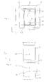
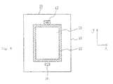
- a reticle 20 includes a rectangular pattern forming area 11 provided in a central portion of a transparent substrate 10 of glass or quartz and formed with a circuit pattern (not shown) and a light shielding area 12 in the form of light shielding film of 1.5 mm wide formed in the periphery of the pattern forming area 11 and surrounding it.
- This location of the light shielding area 12 with respect to the pattern forming area 11 is effective to prevent out of focused light i.e. blurred image from being directed to areas outside a pattern drawing area for one projection exposure when the circuit pattern of the pattern forming area 11 of the reticle 20 is reduced and projected to draw the reduced circuit pattern on the wafer by means of the reduction exposure device.
- a pair of measuring patterns are formed in a center area A of one side (upper side in Fig. 1) 11A of the pattern forming area 11 and a center area B of the opposing side (lower side in Fig. 1) 11B of the area 11, respectively, such that these measuring patterns are centered on a line perpendicular to the sides 11A and 11B. That is, in the portion A, a light shielding pattern having a light transparent pattern 13 of a small area is formed and, in the portion B, a light shielding pattern 14 whose size is larger than that of the light transparent pattern 13 is formed.
- the transparent pattern 13 is rectangular in shape and surrounded by a reversing frame 15 of light shielding film.
- the size of the rectangular light shielding pattern 14 is selected such that the pattern 14 can cover the transparent pattern 13 completely when they are overlapped.
- the shielding pattern 14 is separated from the side 11B by a-distance p.
- a light shielding pattern (not shown) is formed in the pattern forming area surrounding the light shielding pattern 14 by a light shielding film, it is necessary to provide a reverse, transparent frame 26 having no circuit pattern around the light shielding pattern 14. Otherwise, where the light transparent pattern 13 is surrounded by a wide light shielding portion constituting a portion of a pattern formed in the pattern forming area, such reverse frame 15 may be unnecessary. In such case, a portion of the circuit pattern formed in the pattern forming area 11 may serves as the reverse frame 15.
- the light shielding portion of the reticle 20 composed of the light shielding area 12, the reverse frame 15, the light shielding pattern 14 and the circuit pattern (not shown) on the transparent substrate 10 is constituted with a multilayer film composed of a chromium film having thickness of about 80 nm (nano meters) formed directly on the substrate 10 and a chromium oxide film having thickness of about 20 nm formed on the chromium film. It may be possible to form the light shielding portion by using molybdenum silicide.
- the first embodiment there are relatively large light shielding portions around the portions A and B of the reticle 20 and the center positions of the rectangular measuring patterns 13 and 14 are on the straight line parallel to the y axis-of the X-Y stage.
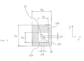
- This embodiment will be described in more detail with an assumption that the reduction rate of the reduction exposure device is 5:1.
- a small light transparent pattern 13 having size in x direction of a x and in y direction of a y it is necessary to provide a light shielding reverse frame 15 therearound, as mentioned previously.
- a light shielding pattern 14 is provided which is larger than the transparent pattern 13 and has size in x direction of b x and in y direction of by.
- the reverse frame 15 can completely cover the light shielding pattern 14 when the center positions of the patterns 13 and 14 are made coincident. Assuming that size of the reverse frame 15 in x direction is m and in y direction is n, m >> b x and n >> b y .
- a x and a y are in the order of 50 ⁇ m
- b x and b y are in the order of 100 ⁇ m
- m and n are in the order of 200 ⁇ m, respectively.
- the reduction exposure device includes various optical systems for obtaining proper alignment of reticle and a signal processing system for processing various-signals therefrom.
- the simplest and reliable way of finally checking a resulting alignment of the reticle set is to project a pattern on the reticle and to check the pattern developed in a photoresist formed on a wafer.
- the exposure is performed usually while moving the X-Y stage with step pitch of X 1 ⁇ m in x direction and Y 1 ⁇ m in y direction. Since the moving error of the X-Y stage in this case can be made small enough (0.02 ⁇ m or lesser), the following description will be done with an assumption that there is substantially no moving error of the X-Y stage.
- the step pitch of the X-Y stage in y direction is made shorter than the usual pitch of Y 1 by S.
- the distance S is set such that the portions A and B of the reticle 20 are overlapped.
- a first shot 16 of the reticle 20 shown in Fig. 1 is projected onto at least one area of the wafer to expose the area.
- a second shot 17 of the same is similarly projected onto an area whose center 21 being remote from the center 19A of the first shot by (Y 1 -S) in y direction; where, Y 1 is the distance between the center 19A of the shot 16 and a center 19B of an adjacent shot 18 to form a circuit pattern.
- the exposed portions A and B of the first and second shots 16 and 17, i.e., the pairs of the measuring patterns are overlapped in a portion C as shown in Fig. 3.
- the measuring patterns 13 and 14 are overlapped and such pattern as shown in Fig. 4 is formed on the wafer.
- photoresist films in a portion 13A which has lengths A x in X direction and A y in Y direction, corresponding to the transparent portion 13 reduced to one fifth and outside of a portion 14A, which has lengths B x in X direction and B y in Y direction, corresponding to the light shielding portion 14 reduced to one fifth are exposed and a photoresist film 25E in the hatched portion therebetween is not exposed.
- the positions of the centers 22, 23 of the reduced transparent pattern 13A and the reduced shielding pattern 14A can be easily measured, respectively, from the configuration of the non-exposed photoresist film 25E and thus the deviations ⁇ x and ⁇ y of the center 23 of the light shielding pattern 14A with respect to the center 22 of the transparent pattern 13A in x and y directions can be measured, respectively.
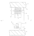
- a pattern formation of this portion C in Fig. 3 and of Fig. 4 will be described with reference to Figs. 5a to 5c.
- the photoresist film 25 formed on the wafer 24 is exposed by the first shot 16, so that there are provided in the photoresist film 25 a non-exposed portion 25A and an exposed portion 25B due to the reverse frame 15 and the transparent pattern 13 of the reticle 20.
- an exposed or non-exposed portion 25C is provided according to the circuit pattern (not shown). Then, as shown in Fig.
- the same wafer is exposed by the second shot 17 with the pitch L', upon which a peripheral portion of the non-exposed portion 25A is exposed by the shielding pattern 14 of the reticle, resulting in an exposed portion 25D. Therefore, only a portion in which the reverse frame 15 and the shielding pattern 14 are overlapped is left as non-exposed portion 25E.
- a positive photoresist film 25 is used as shown in Fig. 5c, the portion of the photoresist film in the exposed portion is disolved by a development leaving the photoresist film portion in the non-exposed portion 25E as the resist pattern 25E on the wafer 24. That is, the photoresist film in the hatched portion in Fig. 4 is left as the resist pattern 25E after the development.
- the centers of the measuring patterns 13 and 14 are arranged on the straight line parallel to the y axis of the X-Y stage. In a case where these centers are on a straight line parallel to the x axis of the X-Y stage, the same explanation as above is applicable by exchanging x and y.
- deviations ⁇ x and ⁇ y shown in Fig. 4 were 0.1 ⁇ m and 0.05 ⁇ m, respectively.
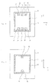
- a second embodiment of the present invention shown in Fig. 6 is similar to the first embodiment except that a plurality pairs (N) of measuring patterns 13 and 14 are provided.
- Fig. 7 is a plan view of a third embodiment of the present invention.
- a transparent pattern 73 and a larger light shielding pattern 74 are circular and centers of these patterns are on a straight line in parallel to y axis of an X-Y stage.
- a reverse frame 75 is large enough in area to completely cover the light shielding pattern 74 and its outer configuration may be any of rectangular as shown, or circular, etc.
- the reason for the necessity of a transparent reverse frame 76 around the light shielding pattern 74 has been described previously with respect to the first embodiment. Other portions of this embodiment are the same as those in the first embodiment.
- a pair of a transparent pattern 13 and a light shielding pattern 14 are formed outside of a light shielding area 12 so that a pattern forming area 11 can be used more effectively.
- An outside portion of the light shielding pattern 14 is of course transparent. Any so long as they are on a straight line in parallel to x or y axis of an X-Y table when the reticle is set.
- the measuring patterns are rectangular or circular, the outer configuration thereof is not limited thereto. That is, the configuration is arbitrary so long as then deviations ⁇ x and ⁇ y of one pattern center with respect to the other in x and y directions can be measured.
Landscapes
- Physics & Mathematics (AREA)
- General Physics & Mathematics (AREA)
- Exposure And Positioning Against Photoresist Photosensitive Materials (AREA)
- Exposure Of Semiconductors, Excluding Electron Or Ion Beam Exposure (AREA)
Claims (5)
- Retikel für Verwendung in einem Step- und Repeat-Verfahren zum Übertragen eines Bauelementmusters auf eine Halbleiterwafer, welches Retikel eine rechteckige Musterbildungsfläche (11), in der das Bauelementmuster gebildet wird, eine Lichtabschirmungsfläche (12), die die Musterbildungsfläche (11) umgibt, und ein Paar von Meßmustern aufweist;
dadurch gekennzeichnet, daß eines der Meßmuster ein durchsichtiges Muster (13) und einen entgegengesetzten Rahmen (15), der das durchsichtige Muster (13) umgibt, und das andere der Meßmuster ein Lichtabschirmungsmuster (14) aufweist, wobei das Retikel von einer ersten Stellung zu einer zweiten Stellung bewegbar ist, wobei das Zentrum des durchsichtigen Musters (13) in der ersten Stellung mit dem Zentrum des lichtabschirmenden Musters (14) in der zweiten Stellung zusammenfällt, so daß der Teil der Wafer, der durch das durchsichtige Muster (13) in der ersten Stellung exponiert wird, in der zweiten Stellung vollständig durch das Lichtabschirmungsmuster (14) bedeckt wird und der Umfang des Teils der Wafer, der durch den entgegengesetzten Rahmen (15) in der ersten Stellung abgeschirmt wird, durch das Lichtabschirmungsmuster (14) in der zweiten Stellung exponiert wird. - Retikel nach Anspruch 1, dadurch gekennzeichnet, daß sowohl das durchsichtige Muster als auch das Lichtabschirmungsmuster vieleckig ist.
- Retikel nach Anspruch 1, dadurch gekennzeichnet, daß sowohl das durchsichtige Muster als auch das lichtabschirmende Muster kreisförmig ist.
- Retikel nach Anspruch 1, 2 oder 3, bei dem das Paar von Meßmustern in dem Musterbildungsbereich ausgebildet ist.
- Retikel nach Anspruch 1, 2 oder 3, dadurch gekennzeichnet, daß das Paar von Meßmustern außerhalb des Lichtabschirmungsbereiches gebildet ist.
Applications Claiming Priority (2)
| Application Number | Priority Date | Filing Date | Title |
|---|---|---|---|
| JP13784990 | 1990-05-28 | ||
| JP137849/90 | 1990-05-28 |
Publications (3)
| Publication Number | Publication Date |
|---|---|
| EP0459737A2 EP0459737A2 (de) | 1991-12-04 |
| EP0459737A3 EP0459737A3 (en) | 1992-09-23 |
| EP0459737B1 true EP0459737B1 (de) | 1998-10-28 |
Family
ID=15208242
Family Applications (1)
| Application Number | Title | Priority Date | Filing Date |
|---|---|---|---|
| EP91304773A Expired - Lifetime EP0459737B1 (de) | 1990-05-28 | 1991-05-28 | Maske für Belichtungsgerät zur verkleinernden Projektion |
Country Status (3)
| Country | Link |
|---|---|
| US (1) | US5237393A (de) |
| EP (1) | EP0459737B1 (de) |
| DE (1) | DE69130407T2 (de) |
Families Citing this family (9)
| Publication number | Priority date | Publication date | Assignee | Title |
|---|---|---|---|---|
| KR100381629B1 (ko) * | 1994-08-16 | 2003-08-21 | 가부시키가이샤 니콘 | 노광장치 |
| US5477058A (en) * | 1994-11-09 | 1995-12-19 | Kabushiki Kaisha Toshiba | Attenuated phase-shifting mask with opaque reticle alignment marks |
| JP3859764B2 (ja) * | 1995-06-27 | 2006-12-20 | 株式会社ルネサステクノロジ | 重ね合わせ精度測定マーク、そのマークの欠陥修正方法、および、そのマークを有するフォトマスク |
| US5876883A (en) * | 1995-12-27 | 1999-03-02 | Vlsi Technology, Inc. | Method forming focus/exposure matrix on a wafer using overlapped exposures |
| US6043164A (en) * | 1996-06-10 | 2000-03-28 | Sharp Laboratories Of America, Inc. | Method for transferring a multi-level photoresist pattern |
| US5914202A (en) * | 1996-06-10 | 1999-06-22 | Sharp Microeletronics Technology, Inc. | Method for forming a multi-level reticle |
| US5753417A (en) * | 1996-06-10 | 1998-05-19 | Sharp Microelectronics Technology, Inc. | Multiple exposure masking system for forming multi-level resist profiles |
| US5887343A (en) * | 1997-05-16 | 1999-03-30 | Harris Corporation | Direct chip attachment method |
| US8689707B2 (en) * | 2006-05-26 | 2014-04-08 | Fuel Tech, Inc. | Ultra low NOx burner replacement system |
Family Cites Families (7)
| Publication number | Priority date | Publication date | Assignee | Title |
|---|---|---|---|---|
| JPS582845A (ja) * | 1981-06-30 | 1983-01-08 | Toshiba Corp | フォトマスク及びパタ−ン評価方法 |
| US4550374A (en) * | 1982-11-15 | 1985-10-29 | Tre Semiconductor Equipment Corporation | High speed alignment method for wafer stepper |
| JPS6085523A (ja) * | 1983-10-17 | 1985-05-15 | Fujitsu Ltd | マスク形成方法 |
| US4771180A (en) * | 1985-10-11 | 1988-09-13 | Matsushita Electric Industrial Co. Ltd. | Exposure apparatus including an optical system for aligning a reticle and a wafer |
| US4842412A (en) * | 1986-01-22 | 1989-06-27 | Eiichi Miyake | Exposure apparatus employed for fabricating printed circuit boards |
| US4849313A (en) * | 1988-04-28 | 1989-07-18 | Vlsi Technology, Inc. | Method for making a reticle mask |
| US4938600A (en) * | 1989-02-09 | 1990-07-03 | Interactive Video Systems, Inc. | Method and apparatus for measuring registration between layers of a semiconductor wafer |
-
1991
- 1991-05-24 US US07/705,130 patent/US5237393A/en not_active Expired - Fee Related
- 1991-05-28 EP EP91304773A patent/EP0459737B1/de not_active Expired - Lifetime
- 1991-05-28 DE DE69130407T patent/DE69130407T2/de not_active Expired - Fee Related
Also Published As
| Publication number | Publication date |
|---|---|
| EP0459737A3 (en) | 1992-09-23 |
| EP0459737A2 (de) | 1991-12-04 |
| DE69130407D1 (de) | 1998-12-03 |
| DE69130407T2 (de) | 1999-03-18 |
| US5237393A (en) | 1993-08-17 |
Similar Documents
| Publication | Publication Date | Title |
|---|---|---|
| JP3197484B2 (ja) | フォトマスク及びその製造方法 | |
| US5451479A (en) | Method of forming a pattern of a multilayer type semiconductor device | |
| US8921013B2 (en) | System and method for test pattern for lithography process | |
| WO1999034255A1 (en) | Method and apparatus for manufacturing photomask and method of fabricating device | |
| JP2001022051A (ja) | レチクル及び半導体装置の製造方法 | |
| JP3292022B2 (ja) | 位置検出装置及びそれを用いた半導体素子の製造方法 | |
| JPS60239022A (ja) | パターン露光方法 | |
| EP0459737B1 (de) | Maske für Belichtungsgerät zur verkleinernden Projektion | |
| JP4613364B2 (ja) | レジストパタン形成方法 | |
| US6569579B2 (en) | Semiconductor mask alignment system utilizing pellicle with zero layer image placement indicator | |
| JP2003156832A (ja) | 収差計測用フォトマスク、収差計測方法、収差計測用装置および装置の製造方法 | |
| JPS5994032A (ja) | 投影露光装置 | |
| US6489067B2 (en) | Reticle for manufacturing semiconductor integrated circuit | |
| JP3028028B2 (ja) | 投影露光装置及びそれを用いた半導体デバイスの製造方法 | |
| US6913858B2 (en) | Photomask for measuring lens aberration, method of manufacturing the same, and method of measuring lens aberration | |
| JP2727784B2 (ja) | 縮小投影露光装置用レティクル | |
| JPS61114529A (ja) | アライメント方法 | |
| US7623219B2 (en) | Exposure apparatus, exposure method, device manufacturing method | |
| JPH0833651B2 (ja) | フォトマスク | |
| CN112034679B (zh) | 一种用于检测曝光机台透镜眩光程度的光掩膜版及方法 | |
| KR0146172B1 (ko) | 노광장치의 렌즈 비점수차 측정방법 | |
| JP3696982B2 (ja) | 半導体集積回路露光用のフォトマスク | |
| JP3529967B2 (ja) | アライメントマーク付きフォトマスク用ブランクスの製造方法 | |
| JP2818391B2 (ja) | 露光装置 | |
| JPH05216209A (ja) | フォトマスク |
Legal Events
| Date | Code | Title | Description |
|---|---|---|---|
| PUAI | Public reference made under article 153(3) epc to a published international application that has entered the european phase |
Free format text: ORIGINAL CODE: 0009012 |
|
| 17P | Request for examination filed |
Effective date: 19910607 |
|
| AK | Designated contracting states |
Kind code of ref document: A2 Designated state(s): DE FR GB |
|
| PUAL | Search report despatched |
Free format text: ORIGINAL CODE: 0009013 |
|
| AK | Designated contracting states |
Kind code of ref document: A3 Designated state(s): DE FR GB |
|
| 17Q | First examination report despatched |
Effective date: 19960918 |
|
| GRAG | Despatch of communication of intention to grant |
Free format text: ORIGINAL CODE: EPIDOS AGRA |
|
| GRAG | Despatch of communication of intention to grant |
Free format text: ORIGINAL CODE: EPIDOS AGRA |
|
| GRAH | Despatch of communication of intention to grant a patent |
Free format text: ORIGINAL CODE: EPIDOS IGRA |
|
| GRAH | Despatch of communication of intention to grant a patent |
Free format text: ORIGINAL CODE: EPIDOS IGRA |
|
| GRAA | (expected) grant |
Free format text: ORIGINAL CODE: 0009210 |
|
| AK | Designated contracting states |
Kind code of ref document: B1 Designated state(s): DE FR GB |
|
| REF | Corresponds to: |
Ref document number: 69130407 Country of ref document: DE Date of ref document: 19981203 |
|
| ET | Fr: translation filed | ||
| PLBE | No opposition filed within time limit |
Free format text: ORIGINAL CODE: 0009261 |
|
| STAA | Information on the status of an ep patent application or granted ep patent |
Free format text: STATUS: NO OPPOSITION FILED WITHIN TIME LIMIT |
|
| 26N | No opposition filed | ||
| REG | Reference to a national code |
Ref country code: GB Ref legal event code: IF02 |
|
| PGFP | Annual fee paid to national office [announced via postgrant information from national office to epo] |
Ref country code: FR Payment date: 20020508 Year of fee payment: 12 |
|
| PGFP | Annual fee paid to national office [announced via postgrant information from national office to epo] |
Ref country code: GB Payment date: 20020522 Year of fee payment: 12 |
|
| PGFP | Annual fee paid to national office [announced via postgrant information from national office to epo] |
Ref country code: DE Payment date: 20020610 Year of fee payment: 12 |
|
| PG25 | Lapsed in a contracting state [announced via postgrant information from national office to epo] |
Ref country code: GB Free format text: LAPSE BECAUSE OF NON-PAYMENT OF DUE FEES Effective date: 20030528 |
|
| PG25 | Lapsed in a contracting state [announced via postgrant information from national office to epo] |
Ref country code: DE Free format text: LAPSE BECAUSE OF NON-PAYMENT OF DUE FEES Effective date: 20031202 |
|
| GBPC | Gb: european patent ceased through non-payment of renewal fee |
Effective date: 20030528 |
|
| PG25 | Lapsed in a contracting state [announced via postgrant information from national office to epo] |
Ref country code: FR Free format text: LAPSE BECAUSE OF NON-PAYMENT OF DUE FEES Effective date: 20040130 |
|
| REG | Reference to a national code |
Ref country code: FR Ref legal event code: ST |