EP0459863A1 - Integrierter Schaltkreis mit Anschlussstift zur Modusfeststellung - Google Patents
Integrierter Schaltkreis mit Anschlussstift zur Modusfeststellung Download PDFInfo
- Publication number
- EP0459863A1 EP0459863A1 EP91401301A EP91401301A EP0459863A1 EP 0459863 A1 EP0459863 A1 EP 0459863A1 EP 91401301 A EP91401301 A EP 91401301A EP 91401301 A EP91401301 A EP 91401301A EP 0459863 A1 EP0459863 A1 EP 0459863A1
- Authority
- EP
- European Patent Office
- Prior art keywords
- spindle
- register
- pin
- resistor
- phases
- Prior art date
- Legal status (The legal status is an assumption and is not a legal conclusion. Google has not performed a legal analysis and makes no representation as to the accuracy of the status listed.)
- Granted
Links
- 238000001514 detection method Methods 0.000 title description 2
- 238000005516 engineering process Methods 0.000 description 4
- 235000021183 entrée Nutrition 0.000 description 2
- 230000015654 memory Effects 0.000 description 2
- 230000001419 dependent effect Effects 0.000 description 1
- 238000012423 maintenance Methods 0.000 description 1
- RONWGALEIBILOG-VMJVVOMYSA-N quinine sulfate Chemical compound [H+].[H+].[O-]S([O-])(=O)=O.C([C@H]([C@H](C1)C=C)C2)C[N@@]1[C@@H]2[C@H](O)C1=CC=NC2=CC=C(OC)C=C21.C([C@H]([C@H](C1)C=C)C2)C[N@@]1[C@@H]2[C@H](O)C1=CC=NC2=CC=C(OC)C=C21 RONWGALEIBILOG-VMJVVOMYSA-N 0.000 description 1
Images
Classifications
-
- G—PHYSICS
- G01—MEASURING; TESTING
- G01R—MEASURING ELECTRIC VARIABLES; MEASURING MAGNETIC VARIABLES
- G01R31/00—Arrangements for testing electric properties; Arrangements for locating electric faults; Arrangements for electrical testing characterised by what is being tested not provided for elsewhere
- G01R31/28—Testing of electronic circuits, e.g. by signal tracer
- G01R31/317—Testing of digital circuits
- G01R31/31701—Arrangements for setting the Unit Under Test [UUT] in a test mode
Definitions
- the invention relates to integrated circuits.
- the classic solution for this consists in applying from the outside a logic level 0 or 1 to the spindle, depending on the mode chosen.
- a detector internal to the integrated circuit examines the state of the spindle and provides the rest of the circuit with an appropriate command which operates the circuit either in one mode or in another depending on the logic level detected.
- the total number of pins of the integrated circuit is thus reduced. This is very important since the price of the integrated circuit is strongly affected by the price of the package and the price of the package is highly dependent on the number of pins.
- An object of the invention is to provide a simple circuit, inexpensive, and consuming little current (especially in steady state), to detect one of three states on a spindle of an integrated circuit.
- the register preferably stores the two logic levels taken by the spindle during the two phases.
- the register then has two outputs which are transmitted to a decoder which supplies the desired output signal used to impose an operating mode of the integrated circuit according to the state of the spindle.
- a buffer stage is interposed between the spindle and the register, and that a switch is provided for disconnecting the spindle from the input of the buffer stage outside the two reading phases and to keep this input at a high or low logic level outside the two reading phases.
- the integrated circuit is preferably produced in CMOS technology to limit the current consumption to the maximum.
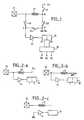
- the pin used to define from the outside a mode of operation of the integrated circuit is designated by the reference 10. It is likely to be placed from the outside in three possible states: low logic state corresponding to a logic voltage level which is for example that of a first supply terminal of the integrated circuit (Vss), high logic state corresponding to a logic level which is that of a second supply voltage (Vcc), or even high impedance state where the terminal is in the air or connected outside the circuit at a very high impedance.
- Pin 10 is connected, inside the integrated circuit, to a state detector which essentially comprises a resistor, switches, and means for detecting the logic level on the pin in two different configurations of switches.
- the state detector comprises a resistor 12 connected on one side to the pin 10, and on the other to the midpoint M of a series assembly of two switches S1 and S2.
- the switch S1 is also connected to a node A whose potential corresponds to the high logic level.
- node A is simply at the high Vcc supply potential.
- the switch S2 is connected to a node B whose potential corresponds to the low logic level; preferably node B is at low supply potential Vss.
- Pin 10 is also connected, via a third switch S3, to a node C which constitutes an input to a buffer amplifier 14 whose output is connected to a register 16 making it possible to record the logic level present on node C.
- a fourth switch makes it possible to put the node C at one of the supply potentials, here the low potential Vss.
- the detector comprises a control means, not shown, for controlling the closing and opening of the switches according to a cycle which will be detailed below, and a small logic circuit 18 for supplying, from the content of the register 16, a representative signal. the state of the spindle, so a signal representative of the operating mode that we want to impose from the outside.
- FIG. 2a a configuration is shown, shown in FIG. 2a, in which the pin is connected on the one hand to the input of the amplifier 14 and on the other hand to Vcc via the resistor 12. If the spindle is kept from the outside at the low logic level Vss, it is this level which is transmitted via the amplifier to the register 16; the register takes this level in memory; if the spindle is at Vcc, it is the high logic level which is transmitted and stored in the register; if finally the spindle is outside at high impedance, it is connected to Vcc by the resistor whose value R is much lower than the high external impedance; it is therefore still the high logic level Vcc which is transmitted and stored in the register 16.
- the state of the spindle if there is a low state in the register twice, it means that the spindle was in the low state; if we have twice a high state, it is because the spindle was in the high state; but if we have once a high state and once a low state, it means that the spindle was in high impedance during reading.
- the outputs A1 and A2 of the register representing the logic states of the spindle during the two reading phases, are therefore combined in a small logic circuit 18 which is a decoder providing for example three outputs B1, B2, B3 each representing a respective state of spindle 10. These outputs B1, B2, B3 are used to modify internal functionalities of the integrated circuit so as to pass it into a particular operating mode.
- each pin is connected to a detector such as that of FIG. 1, but the logic circuit 18 can be a common circuit decoding the combination of states noted in the registers such as 16.
- the resistor 12 can have a value of the order of 10 kilohms, but its value is not critical, provided that it is low enough to properly pull the spindle at potential Vss or Vcc when the spindle is at high impedance, and not too low so as not to hinder the maintenance of the spindle from the outside at a determined potential when the spindle is not at high impedance.
Landscapes
- Engineering & Computer Science (AREA)
- General Engineering & Computer Science (AREA)
- Physics & Mathematics (AREA)
- General Physics & Mathematics (AREA)
- Logic Circuits (AREA)
- Semiconductor Integrated Circuits (AREA)
Applications Claiming Priority (2)
| Application Number | Priority Date | Filing Date | Title |
|---|---|---|---|
| FR9006717 | 1990-05-30 | ||
| FR9006717A FR2662874B1 (fr) | 1990-05-30 | 1990-05-30 | Circuit integre avec broche de detection de mode. |
Publications (2)
| Publication Number | Publication Date |
|---|---|
| EP0459863A1 true EP0459863A1 (de) | 1991-12-04 |
| EP0459863B1 EP0459863B1 (de) | 1993-07-21 |
Family
ID=9397092
Family Applications (1)
| Application Number | Title | Priority Date | Filing Date |
|---|---|---|---|
| EP91401301A Expired - Lifetime EP0459863B1 (de) | 1990-05-30 | 1991-05-21 | Integrierter Schaltkreis mit Anschlussstift zur Modusfeststellung |
Country Status (4)
| Country | Link |
|---|---|
| US (1) | US5198707A (de) |
| EP (1) | EP0459863B1 (de) |
| DE (1) | DE69100181T2 (de) |
| FR (1) | FR2662874B1 (de) |
Cited By (1)
| Publication number | Priority date | Publication date | Assignee | Title |
|---|---|---|---|---|
| US7199653B2 (en) * | 2005-08-24 | 2007-04-03 | Fujitsu Limited | Semiconductor device with operation mode set by external resistor |
Families Citing this family (15)
| Publication number | Priority date | Publication date | Assignee | Title |
|---|---|---|---|---|
| USRE36443E (en) * | 1988-10-31 | 1999-12-14 | Sgs-Thomson Microelectronics, Inc. | Dialer with internal option select circuit programmed with externally hardwired address |
| US5477166A (en) * | 1993-04-22 | 1995-12-19 | Benchmarq Microelectronics | Programmable output device with integrated circuit |
| US5457411A (en) * | 1994-12-02 | 1995-10-10 | Texas Instruments Incorporated | Trinary logic input gate |
| US5629635A (en) * | 1995-09-26 | 1997-05-13 | Ics Technologies, Inc. | Address programming via LED pin |
| US6134686A (en) * | 1998-05-29 | 2000-10-17 | Cypress Semiconductor Corp. | Technique to detect drive strength of input pin |
| US6127851A (en) * | 1999-01-26 | 2000-10-03 | International Business Machines Corporation | Circuit and method for differentiating multiple modules |
| US6338099B1 (en) * | 1999-07-09 | 2002-01-08 | Behavior Tech Computer Corp. | Device code recognizing circuit |
| US20040040652A1 (en) * | 2002-08-30 | 2004-03-04 | 3M Innovative Properties Company | Methods for electrostatically adhering an article to a substrate |
| US6788095B1 (en) * | 2003-01-31 | 2004-09-07 | Xilinx, Inc. | Method for gross input leakage functional test at wafer sort |
| US7098833B2 (en) * | 2004-06-04 | 2006-08-29 | Texas Instruments Incorporated | Tri-value decoder circuit and method |
| TWI269529B (en) * | 2005-06-14 | 2006-12-21 | Richtek Technology Corp | Tri-state output logic with zero quiescent current by one input control |
| CN101197569B (zh) * | 2006-12-07 | 2011-04-06 | 立锜科技股份有限公司 | 内建于芯片用于设定芯片操作模式的电路及方法 |
| JP5301262B2 (ja) | 2008-12-19 | 2013-09-25 | ルネサスエレクトロニクス株式会社 | 半導体装置、及び動作モ−ド切換方法 |
| US12111339B2 (en) * | 2021-11-19 | 2024-10-08 | Richtek Technology Corporation | State detection circuit for detecting tri-state and state detection method thereof |
| TWI796241B (zh) * | 2021-11-19 | 2023-03-11 | 立錡科技股份有限公司 | 具三態偵測功能之狀態偵測電路及其狀態偵測方法 |
Citations (2)
| Publication number | Priority date | Publication date | Assignee | Title |
|---|---|---|---|---|
| EP0141681A2 (de) * | 1983-11-07 | 1985-05-15 | Texas Instruments Incorporated | Schaltung zur Erfassung von Prüfeingaben |
| US4837505A (en) * | 1985-11-20 | 1989-06-06 | Ricoh Company, Ltd. | Test mode activation circuit |
Family Cites Families (6)
| Publication number | Priority date | Publication date | Assignee | Title |
|---|---|---|---|---|
| US4005315A (en) * | 1975-09-22 | 1977-01-25 | Signetics Corporation | Triple state to binary converter |
| JPS5284938A (en) * | 1976-01-07 | 1977-07-14 | Hitachi Ltd | Logic circuit |
| JPS52146534A (en) * | 1976-05-31 | 1977-12-06 | Toshiba Corp | Input circuit |
| JPS56153840A (en) * | 1980-04-28 | 1981-11-28 | Oki Electric Ind Co Ltd | Ternary level input circuit |
| JPS58202628A (ja) * | 1982-05-20 | 1983-11-25 | Sharp Corp | 3値レベル入力回路 |
| FR2636797B1 (fr) * | 1988-09-16 | 1990-11-09 | Sgs Thomson Microelectronics | Circuit integre pour poste telephonique avec detecteur d'enveloppe de signal |
-
1990
- 1990-05-30 FR FR9006717A patent/FR2662874B1/fr not_active Expired - Lifetime
-
1991
- 1991-05-21 DE DE91401301T patent/DE69100181T2/de not_active Expired - Fee Related
- 1991-05-21 EP EP91401301A patent/EP0459863B1/de not_active Expired - Lifetime
- 1991-05-24 US US07/705,375 patent/US5198707A/en not_active Expired - Lifetime
Patent Citations (2)
| Publication number | Priority date | Publication date | Assignee | Title |
|---|---|---|---|---|
| EP0141681A2 (de) * | 1983-11-07 | 1985-05-15 | Texas Instruments Incorporated | Schaltung zur Erfassung von Prüfeingaben |
| US4837505A (en) * | 1985-11-20 | 1989-06-06 | Ricoh Company, Ltd. | Test mode activation circuit |
Cited By (1)
| Publication number | Priority date | Publication date | Assignee | Title |
|---|---|---|---|---|
| US7199653B2 (en) * | 2005-08-24 | 2007-04-03 | Fujitsu Limited | Semiconductor device with operation mode set by external resistor |
Also Published As
| Publication number | Publication date |
|---|---|
| FR2662874B1 (fr) | 1992-08-07 |
| FR2662874A1 (fr) | 1991-12-06 |
| DE69100181T2 (de) | 1994-02-10 |
| US5198707A (en) | 1993-03-30 |
| EP0459863B1 (de) | 1993-07-21 |
| DE69100181D1 (de) | 1993-08-26 |
Similar Documents
| Publication | Publication Date | Title |
|---|---|---|
| EP0459863B1 (de) | Integrierter Schaltkreis mit Anschlussstift zur Modusfeststellung | |
| EP1200927A1 (de) | Chipkarten-lesegerät mit energiespareinrichtung | |
| FR2667169A1 (fr) | Circuit de production de haute tension pour un circuit de memoire a semiconducteur. | |
| FR2776410A1 (fr) | Dispositifs pour masquer les operations effectuees dans une carte a microprocesseur | |
| FR2686998A1 (fr) | Carte a puce a plusieurs protocoles de communication. | |
| FR2634299A1 (fr) | Circuit de reconnaissance de codes sequentiels programmables | |
| EP0500461B1 (de) | Anordnung für die Detektion des logischen Zustandes eines Bauteiles, dessen Impedanz sich in Abhängigkeit von seinen Zustand ändert | |
| FR2466906A1 (fr) | Circuit detecteur de transitions d'un niveau de signal a un autre | |
| FR2743959A1 (fr) | Dispositif de transmission multidirectionnelle de donnees | |
| FR2692072A1 (fr) | Bascule bistable à commande de réinitialisation. | |
| EP0442829B1 (de) | Taktfrequenzverdoppler | |
| EP0051525A1 (de) | Logische Anordnung mit vereinfachter elektrischer Programmierung | |
| FR2742870A1 (fr) | Systeme de detection de presence d'un objet conducteur d'electricite, notamment un circuit integre present sur une carte a puce | |
| FR2793064A1 (fr) | Memoire a courant de fuite reduit | |
| FR2756120A1 (fr) | Dispositif de conversion serie/parallele d'un signal haute frequence de faible amplitude | |
| EP0537083A1 (de) | Anordnung zum Lesen eines Speicherzelleinhalts, insbesondere für ein EPROM, Betriebsverfahren und Speicher mit solcher Schaltung | |
| FR2750547A1 (fr) | Systeme de commutation entre des etats de veille et de reveil, d'une unite de traitement d'informations et d'un commutateur analogique | |
| FR2810438A1 (fr) | Circuit de detection d'usure | |
| EP0130129B1 (de) | Festwertspeicher organisiert in zwei Halbflächen für Lesegeschwindigkeit | |
| EP0865164A1 (de) | Konvertershaltung für analoge Pegel | |
| EP0568474B1 (de) | MOS-Schaltung zum Extrahieren eines Synchronisierungssignals in einem BAS-Videosignal | |
| EP0772853B1 (de) | Alarmdetektoren für geäudeüberwachung | |
| EP0594478B1 (de) | Anwendungsspezifische Integrierte Schaltung mit einem Mikroprozessor und Prüfmitteln | |
| EP1233402A1 (de) | Gerät zur Verarbeitung graphischer Muster mit unterschiedlichen Formaten durch Pixelextraktion und Leitweglenkung zu unterschiedlichen Kodiermitteln | |
| FR2732133A1 (fr) | Detecteur de coherence d'informations contenues dans un circuit integre |
Legal Events
| Date | Code | Title | Description |
|---|---|---|---|
| PUAI | Public reference made under article 153(3) epc to a published international application that has entered the european phase |
Free format text: ORIGINAL CODE: 0009012 |
|
| AK | Designated contracting states |
Kind code of ref document: A1 Designated state(s): DE FR GB IT |
|
| 17P | Request for examination filed |
Effective date: 19911024 |
|
| 17Q | First examination report despatched |
Effective date: 19920311 |
|
| ITF | It: translation for a ep patent filed | ||
| GRAA | (expected) grant |
Free format text: ORIGINAL CODE: 0009210 |
|
| AK | Designated contracting states |
Kind code of ref document: B1 Designated state(s): DE FR GB IT |
|
| REF | Corresponds to: |
Ref document number: 69100181 Country of ref document: DE Date of ref document: 19930826 |
|
| GBT | Gb: translation of ep patent filed (gb section 77(6)(a)/1977) |
Effective date: 19931015 |
|
| PLBE | No opposition filed within time limit |
Free format text: ORIGINAL CODE: 0009261 |
|
| STAA | Information on the status of an ep patent application or granted ep patent |
Free format text: STATUS: NO OPPOSITION FILED WITHIN TIME LIMIT |
|
| 26N | No opposition filed | ||
| PGFP | Annual fee paid to national office [announced via postgrant information from national office to epo] |
Ref country code: GB Payment date: 20000517 Year of fee payment: 10 |
|
| PGFP | Annual fee paid to national office [announced via postgrant information from national office to epo] |
Ref country code: DE Payment date: 20000522 Year of fee payment: 10 |
|
| PGFP | Annual fee paid to national office [announced via postgrant information from national office to epo] |
Ref country code: FR Payment date: 20010518 Year of fee payment: 11 |
|
| PG25 | Lapsed in a contracting state [announced via postgrant information from national office to epo] |
Ref country code: GB Free format text: LAPSE BECAUSE OF NON-PAYMENT OF DUE FEES Effective date: 20010521 |
|
| GBPC | Gb: european patent ceased through non-payment of renewal fee |
Effective date: 20010521 |
|
| PG25 | Lapsed in a contracting state [announced via postgrant information from national office to epo] |
Ref country code: DE Free format text: LAPSE BECAUSE OF NON-PAYMENT OF DUE FEES Effective date: 20020301 |
|
| PG25 | Lapsed in a contracting state [announced via postgrant information from national office to epo] |
Ref country code: FR Free format text: LAPSE BECAUSE OF NON-PAYMENT OF DUE FEES Effective date: 20030131 |
|
| REG | Reference to a national code |
Ref country code: FR Ref legal event code: ST |
|
| PG25 | Lapsed in a contracting state [announced via postgrant information from national office to epo] |
Ref country code: IT Free format text: LAPSE BECAUSE OF NON-PAYMENT OF DUE FEES;WARNING: LAPSES OF ITALIAN PATENTS WITH EFFECTIVE DATE BEFORE 2007 MAY HAVE OCCURRED AT ANY TIME BEFORE 2007. THE CORRECT EFFECTIVE DATE MAY BE DIFFERENT FROM THE ONE RECORDED. Effective date: 20050521 |