EP0460165B1 - Procede et appareil pour verifier un systeme de coussin pneumatique de securite - Google Patents
Procede et appareil pour verifier un systeme de coussin pneumatique de securite Download PDFInfo
- Publication number
- EP0460165B1 EP0460165B1 EP91901416A EP91901416A EP0460165B1 EP 0460165 B1 EP0460165 B1 EP 0460165B1 EP 91901416 A EP91901416 A EP 91901416A EP 91901416 A EP91901416 A EP 91901416A EP 0460165 B1 EP0460165 B1 EP 0460165B1
- Authority
- EP
- European Patent Office
- Prior art keywords
- capacitor
- value
- voltage value
- monitoring
- squib
- Prior art date
- Legal status (The legal status is an assumption and is not a legal conclusion. Google has not performed a legal analysis and makes no representation as to the accuracy of the status listed.)
- Expired - Lifetime
Links
- 238000012360 testing method Methods 0.000 title claims abstract description 113
- 238000000034 method Methods 0.000 title claims description 21
- 239000003990 capacitor Substances 0.000 claims abstract description 211
- 238000007599 discharging Methods 0.000 claims abstract description 16
- 238000012544 monitoring process Methods 0.000 claims description 63
- 239000002131 composite material Substances 0.000 claims description 6
- 239000007787 solid Substances 0.000 claims 42
- 238000005259 measurement Methods 0.000 description 15
- 230000001934 delay Effects 0.000 description 8
- 238000004364 calculation method Methods 0.000 description 5
- 238000004458 analytical method Methods 0.000 description 2
- 238000006243 chemical reaction Methods 0.000 description 2
- 238000013461 design Methods 0.000 description 2
- 238000002405 diagnostic procedure Methods 0.000 description 2
- 230000000694 effects Effects 0.000 description 2
- 238000004519 manufacturing process Methods 0.000 description 2
- 230000003068 static effect Effects 0.000 description 2
- 238000013459 approach Methods 0.000 description 1
- 238000010304 firing Methods 0.000 description 1
- 230000006870 function Effects 0.000 description 1
- 238000010998 test method Methods 0.000 description 1
Images



Classifications
-
- B—PERFORMING OPERATIONS; TRANSPORTING
- B60—VEHICLES IN GENERAL
- B60R—VEHICLES, VEHICLE FITTINGS, OR VEHICLE PARTS, NOT OTHERWISE PROVIDED FOR
- B60R21/00—Arrangements or fittings on vehicles for protecting or preventing injuries to occupants or pedestrians in case of accidents or other traffic risks
- B60R21/01—Electrical circuits for triggering passive safety arrangements, e.g. airbags, safety belt tighteners, in case of vehicle accidents or impending vehicle accidents
- B60R21/017—Electrical circuits for triggering passive safety arrangements, e.g. airbags, safety belt tighteners, in case of vehicle accidents or impending vehicle accidents including arrangements for providing electric power to safety arrangements or their actuating means, e.g. to pyrotechnic fuses or electro-mechanic valves
- B60R21/0173—Diagnostic or recording means therefor
- B60R21/0176—Diagnostic or recording means therefor for firing circuits using only mechanical switches as collision detecting means, in series with pyrotechnic fuses
Definitions
- the present invention relates to diagnostic testing of an airbag restraint system and is particularly directed to a method and apparatus for testing (i) the operativeness of a storage capacitor and (ii) the impedance values of inertia switch resistors in an airbag restraint system.
- Airbag restraint systems for passenger vehicles are known in the art.
- Such systems typically include an actuation circuit and a diagnostic circuit.
- the actuation circuit includes at least one inertia switch connected in series with a detonating device, e.g., a squib, and a source of electrical energy.
- the diagnostic circuit tests the operativeness of the actuation circuit and controls actuation of an indicator to inform the vehicle operator of a detected system error.
- Such diagnostic circuits typically monitor voltage values at various test points in the actuation circuit and compares the monitored voltage values against predetermined limits. When a monitored voltage value is outside of its predetermined limits, a system error has occurred.
- Airbag restraint systems receive their operating power from the vehicle battery. When vehicle deceleration exceeds a value sufficient to close the inertia switches in the restraint system, e.g., during a vehicle crash, a squib is "fired" and the airbag is inflated. The battery provides the electrical energy to fire a squib.
- Typical airbag restraint systems include a storage capacitor that functions as either a main power source or as a back-up power source should the actuation circuit become disconnected from the vehicle battery during a crash.
- the storage capacitor in such airbag restraint systems must have a sufficient capacitance value to insure that an adequate supply of electrical energy will be available to fire the squib.
- Some prior art diagnostic circuits monitor the static, steady-state voltage developed across the capacitor. An incorrect capacitance value, however, cannot be detected by simply monitoring the static steady-state voltage developed across the capacitor.
- U.S. Patent No. 3,714,627 discloses a diagnostic circuit for an airbag restraint system that tests the operativeness of a storage capacitor.
- the voltage developed at a connection terminal of the storage capacitor is compared to the charge voltage developed across a test capacitor during initial energization of the restraint system. If the voltage value at the terminal of the storage capacitor is greater than the charge across the test capacitor during this initial energization period, such occurrence indicates that the storage capacitor is open circuited. An error indication is provided to the vehicle operator upon such occurrence.
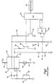
- a squib 10 has one terminal connected to electrical ground through an 0.1 Ohm resistor 12. The other terminal of the squib 10 is connected to capacitors 14, 16.
- Capacitor 14 is connected to a source of electrical energy V(up) through a diode 18 and a current limiting resistor 20.
- Capacitor 16 is connected to the source of electrical energy V(up) through a diode 18 and a current limiting resistor 22.
- the capacitors 14, 16 charge through the squib 10.
- a voltage is developed across each capacitor 14, 16 substantially equal to V(up).
- the current limiting resistors 20, 22 prevent the squib 10 from "firing" during the charging of the capacitors 14, 16.
- the capacitors 14, 16 are connected to one terminal of an inertia switch 24 through diodes 26, 28, respectively.
- the other terminal of inertia switch 24 is connected to electrical ground.
- a resistor 29 is connected in parallel with the inertia switch 24.
- the capacitors 14, 16 arc further connected to field-effect-transistors ("FETs") 30, 32 through resistors 34, 36, respectively.
- FETs field-effect-transistors
- Each FET 30, 32 is controllably connected to a microcomputer 38.
- the junction of resistor 20 and capacitor 14 is connected to a voltage dividing network 40 including resistors 42, 44 connected in series to electrical ground.
- the junction of resistor 22 and capacitor 16 is connected to a voltage dividing network 46 including resistors 48, 50 connected in series to electrical ground.
- the junction of resistors 42, 44 is connected to an analog-to-digital ("A/D") converter 52.
- the junction of resistors 48, 50 is connected to the A/D converter 52.
- the A/D converter is operatively connected to the microcomputer 38.
- the microcomputer 38 is connected to an indicator 54.
- the circuit shown in Figure 1 tests the operativeness of capacitors 14, 16, serially, i.e., separately.
- the microcomputer 38 partially discharges one of the capacitors being tested.
- the microcomputer monitors the voltage across the capacitor being tested through its associated resistor network 40, 46 and its associated connection with the A/D converter 52. If the monitored voltage across the capacitor being tested, which is now partially discharged, is not greater than a predetermined limit, e.g., as would occur when the capacitor is open circuited or is not a proper value, the indicator 54 is energized to warn the vehicle operator of the detected error.
- the capacitor test in the system shown in Figure 1 requires a separate switching FET for each capacitor and a separate voltage dividing network connected to the A/D converter for each capacitor. Also, each capacitor test is time consuming. Because each airbag restraint system must be fully tested during the manufacturing process, such a long period of time needed to complete a test sequence is not desirable. It is, therefore, desirable to decrease the time needed for completion of a test sequence to decrease manufacturing time of the system.
- each inertia switch in known airbag restraint systems includes an associated resistor connected in parallel therewith.
- Each inertia switch resistor is connected in series with other inertia switch resistors of the system and with the squib.
- the inertia switch resistors and the squib form a voltage dividing network.
- a monitoring circuit monitors the voltage at connection terminals of the inertia switches. Based upon the monitored voltage values, the monitoring circuit determines if an inertia switch is electrically short circuited or electrically open circuited.
- inertia switch resistors must be sufficient to limit the steady state current flow through the squib to a value well below that required to "fire" the squib. It is, therefore, desirable to be able to accurately measure the impedance of each inertia switch resistor to determine if its value is within predetermined limits.
- the present invention provides a new and improved method and apparatus for testing an airbag restraint system.
- the invention provides an accurate determination of the operativeness of a storage capacitor in an airbag restraint system of the type having first and second inertia switches, one connected to each side of a squib.
- the invention also provides an accurate determination of the value of parallel connected inertia switch resistors.
- the invention is defined in claims 1, 5, 9, 12, 15, 17, 19, 20, 21, 22, 23, 25.
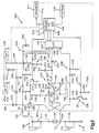
- the circuit 100 includes a squib 102 having a first terminal 104 connected to a first inertia switch assembly 106.
- the squib 102 includes a second terminal 108 connected to a second inertia switch assembly 110.
- the inertia switch assembly 106 includes a normally open inertia switch 112 and a parallel connected resistor 114.
- the assembly 106 is referred to as the safing sensor.
- the inertia switch assembly 110 includes a normally open inertia switch 116 and a parallel connected resistor 118.
- the assembly 110 is referred to as the front sensor.
- the safing sensor is located on the interior compartment of the vehicle and the front sensor is located at a remote location near the front of the vehicle.
- the front sensor 110 has its second terminal connected to electrical ground.
- the second terminal 134 of the safing sensor 106 is connected to the vehicle battery 117 through the vehicle's ignition switch 119 and a diode 120.
- the second terminal 134 of the safing sensor is also connected to the output of a voltage up converter 122 through the series connection of a diode 124, resistor 126, and diode 128.
- the value of the output voltage from V up 122 is substantially greater than the value of the battery voltage received through the ignition switch.
- the V up voltage is used to charge capacitor 130 connected between the junction of resistor 126 and diode 128 and electrical ground. It will be appreciated that the voltage charge on the capacitor 130 is equal to the value of the V up voltage minus the voltage drop across diode 124 and resistor 126.
- a voltage present at terminal 134 which is the cathode side of diode 128, is equal to the voltage charge on capacitor 130 minus the value of the voltage drop across the diode 128.
- the voltage present at terminal 134 is referred to as V C .
- V C under normal operation, is substantially greater than the value of the battery voltage so that the diode 120 is reversed biased.
- resistors 114 and 118 are sufficient to maintain a steady-state current flow through the squib 102 which is substantially less than that necessary to fire the squib.
- the resistors 114, 118 in combination with the squib 102 form a voltage dividing network.
- a voltage value is present at terminals 104, 108 which is a ratiometric division of the voltage V C .
- the resistance value of the squib 102 is approximately 2 ohms.
- the resistance values of resistors 114, 118 are typically 5 kohms each. Therefore, a voltage will be present at terminals 104, 108 equal to approximately 1/2 the voltage V C .
- An analog-to-digital converter (“A/D") 140 is used to monitor the voltage values at various test points within the circuit 100.
- a first input 142 of A/D converter 140 is connected to the output of the voltage up converter 122 through a resistor divider network 144 which includes resistors 146, 148 connected between the output of the voltage up converter 122 and electrical ground.
- a filter capacitor 150 is connected between the junction of resistors 146, 148 and electrical ground.
- a second input 152 of A/D converter 140 is connected to the voltage V C at terminal 134 through a resistor dividing network 154 which includes resistors 156, 158 connected in series between the terminal 134 and electrical ground.
- a filter capacitor 160 is electrically connected between the junction of resistors 156, 158 and electrical ground.
- a differential amplifier circuit 170 is used to monitor the voltage developed across the squib 102.
- the differential amplifier circuit 170 includes an operational amplifier 172 having its noninverting input 174 connected to the terminal 108 through a resistor 176.
- the noninverting input 174 is also connected to a DC electrical energy source, designated V cc , through a resistor 178.
- Voltage V cc is used to bias the noninverting input 174.
- Noninverting input 174 is further connected to a filter capacitor 180.
- the second terminal of capacitor 180 is connected to electrical ground.
- the inverting input 182 of the operational amplifier 172 is connected to terminal 104 through a resistor 184.
- the operational amplifier 172 includes an output 186 which is electrically connected to the inverting input 182 through a parallel connection of a resistor 188 and a capacitor 190.
- the power supply connection terminals 192, 194 of the operational amplifier 172 are connected to the output of the voltage up converter V up 122 and electrical ground, respectively.
- the output 186 of the operational amplifier 172 is connected to an input terminal 196 of the A/D converter 140 through series connected resistors 200 and 202.
- a filter capacitor 204 is connected between one terminal of resistor 202 and electrical ground.
- a diode 205 has its anode connected to the junction of resistors 200, 202 and its cathode connected to V cc . The purpose of diode 205 is to prevent over voltages from being applied to the input 196 of the A/D 140 upon power down of the circuit 100.
- the detailed operation of the differential amplifier circuit 170 is fully described in U.S. Patent No. 4,825,148, issued April 25, 1989 to McCurdy et al., and assigned to the assignee of the present application, the disclosure of which is hereby fully incorporated herein by reference.
- An input terminal 206 of A/D converter 140 is connected to terminal 108 through a resistor dividing network 208 which includes resistors 210, 212 connected in series between the junction 108 and electrical ground.
- a filter capacitor 214 is electrically connected between the junction of resistors 210, 212 and electrical ground.
- the voltage value present at the terminal 108 is referred to as V F .
- the output 186 of the operational amplifier 172 is referred to as V S .
- the A/D converter 140 is operatively connected to a microcomputer 250.
- the connection with and cooperation between an A/D converter and a microcomputer are well known in the art and therefore will not be described in detail herein.
- the microcomputer addresses an input of the A/D converter.
- the A/D converter serially outputs a binary number to the microcomputer wherein the number is indicative of the analog voltage present at the addressed input.
- the microcomputer 250 is programmed with algorithms that account for the values of divide-down resistors present in the circuit 100. For example, when measuring the voltage V F at terminal 108, the voltage present at the input 206 of the A/D converter 140 is divided by resistors 210, 212.
- the microcomputer 250 accounts for the divide-down resistors in its determination of the voltage value present at terminal 108.
- a first switching circuit 260 is electrically connected in parallel with the safing sensor 106.
- the switching circuit 260 includes a PNP transistor 262 having its emitter connected to the terminal 134.
- the collector of transistor 262 is connected to terminal 104 through a resistor 264.
- the base of transistor 262 is connected to the terminal 134 through a resistor 266.
- the base of transistor 262 is further connected to the collector of an NPN transistor 270 through a resistor 272.
- the emitter of transistor 270 is connected to electrical ground.
- the base of transistor 270 is electrically connected to an output 274 of microcomputer 250 through a resistor dividing network 276.
- the resistor dividing network 276 includes resistors 278, 280 connected in series between the output 274 and electrical ground.
- the base of transistor 270 is connected to the junction of resistors 278, 280.
- a second switching circuit 290 is connected in parallel with the front sensor 110.
- the second switching circuit 290 includes an NPN transistor 292 having its collector connected to the terminal 108 through a resistor 294.
- the emitter of transistor 292 is connected to electrical ground.
- the babe of transistor 292 is connected to an output 298 of microcomputer 250 through a resistor dividing network 300.
- the resistor dividing network 300 includes resistors 302, 304 connected in series between the output 298 of microcomputer 250 and electrical ground.
- the base of transistor 292 is connected to the junction of resistors 302, 304.
- the transistors 262, 292 are respectively referred to as Q1, Q2.
- the microcomputer 250 controls actuation of the transistors Q1, Q2 so as to selectively place resistors 264, 294 in parallel with resistors 114, 118, respectively.
- the microcomputer 250 further includes an output 310 connected to an indicator 312 located within the vehicle compartment and clearly visible to the vehicle operator.
- the indicator 312 is used to provide an indication to the vehicle operator of a detected error within the circuit 100.
- the microcomputer 250 further includes an output 316 electrically connected to a nonvolatile memory 318, such as an electrically erasable, programmable read only memory (“EEPROM").
- EEPROM electrically erasable, programmable read only memory
- the EEPROM is used to record failure information for later analysis by service technicians.
- the present invention provides an accurate measurement of the impedance value of each of the inertia switch resistors 114, 118, tests the operativeness of capacitor 130 to insure that the capacitor is properly connected, and test that the capacitor has a correct, or, at least, a minimum capacitance value.
- the circuit 100 performs the resistor and capacitor tests in parallel, i.e., the two tests are performed simultaneously.
- a capacitor short test is also performed by monitoring the voltage value V C through input 152 of A/D converter 140. If the microcomputer 250 determines V C ⁇ 18 VDC, the capacitor 130 is considered to be short circuited.
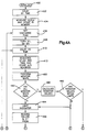
- step 400 the system is initially powered up upon the vehicle operator starting the vehicle.
- the microcomputer 250 delays any further operation of the circuit 100 for an amount of time X1.
- the time delay X1 is sufficient to insure that the capacitor 130 is fully charged. This delay occurs in step 402.
- step 404 the microcomputer measures the value of the voltage V C present at terminal 134 and measures the value of the voltage V up . Both measured values are stored in the microcomputer's internal memory 405.
- the capacitor is partially discharged, i.e., permitted to discharge over a predetermined time period.
- the microcomputer sets a discharge flag in step 406 and turns ON both transistors Q1 and Q2 in step 408.
- resistor 264 is in parallel with resistor 114 and resistor 294 is in parallel with resistor 118. This parallel resistor combination results in a drop in the value of voltage V C present at terminal 134.
- the transistors Q1 and Q2 are turned ON at time T0 and are turned OFF at time T1, the voltage V C will drop by an amount equal to ⁇ V. If at time T1, the transistors Q1 and Q2 are both turned OFF, the capacitor 130 begins to charge up to the value which is V up minus the voltage drop across diode 124 and resistor 126. If the capacitance value of capacitor 130 is greater than a predetermined minimum, the voltage drop ⁇ V will be less than a predetermined maximum value. At time T1, the microcomputer can monitor the voltage at V C . If the voltage drop ⁇ V from time T0 to T1 is greater than the predetermined limit, then such is an indication that the capacitance value of capacitor 130 is less than a predetermined minimum.
- V C (T 0 ) - V C (T 1 ) ⁇ limit 1 provides adequate accuracy to diagnose low capacitance, i.e., a capacitance value of less than a predetermined value.
- the accuracy of this test measurement is functionally related to the value of V up and V cc , which serves as the ratiometric reference of the A/D 140, but not the values of resistors 156 and 158.
- the tolerance variations of resistors 156 and 158 is effectively cancelled out by the calculation.
- the effect of this division is to substantially cancel out ratiometric variations in V cc , V up , and the voltage drops across diodes 124 and 128.
- the only significant variance remaining results in the uncertainty in the A/D conversion and truncation errors associated with the divide operation in the microcomputer 250.
- the preferred algorithm mathematically reduces equation (2) to: V C (T 1 ) V C (T 0 ) ⁇ 256 ⁇ Limit 3 which further reduces the variability of the solution to uncertainty in the A/D conversion.
- This capacitance test can be considered an adjusted test, i.e., adjusted for variations in V cc , V up , and the voltage drops across diodes 124, 128.
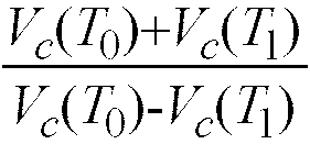
- Equation (8) can be rewritten as: C ⁇ t 2R ⁇ V C (T 0 ) + V C (T 1 ) V C (T 0 ) - V C (T 1 ) - 2V f V C (T 0 ) - V C (T 1 ) where C is capacitance, t is the discharge time (T1 - T0), and R is the equivalent charge/discharge composite resistance.
- V up and V cc are at their nominal values, a nominal result will be calculated. If the V up voltage is higher than nominal, V C will also be higher than nominal, and the A/D readings for both V C (T0) and V C (T1) will increase proportionally. The division effectively cancels out the increase in V up and variations in V cc . As a result, the division of V C (T0) by V C (T1) is automatically compensated for normal variations in circuit components.
- the capacitor 130 must be of sufficient capacitance value to insure that a sufficient amount of electrical energy will be available to fire the squib 102.
- the electrical energy supplied by the capacitor must be available for a predetermined amount of time after the battery becomes disconnected from V up and the ignition switch 119. Therefore, the capacitance value of capacitor 130 is substantial.
- the discharge/charge cycle depicted in Fig. 3A typically takes seven seconds to complete. Applicants have found that it is possible to test other portions of the control circuit simultaneous with the testing of the capacitor 130.
- the microcomputer delays an amount of time X2 in step 410 after the transistors Q1, Q2 are both turned ON.
- the delay time X2 is depicted as the time between T0 and T A .
- the microcomputer begins to sequence Q1 and Q2 through various ON and OFF states. The voltage values at each switched state are measured and stored for later use. The detail of step 412 is shown in the flow chart of Fig. 5.
- step 420 the microcomputer 250 turns Q1 and Q2 OFF. After Q1 and Q2 are turned OFF, the microcomputer delays a predetermined amount of time in step 422. Referring to Fig. 3B, transistors Q1 and Q2 turning OFF occurs at time T A and the delay time is equal to the amount of time between T A and T B .
- the microcomputer in step 424 reads the voltage values present at all the A/D input channels and stores these values in its memory 405. The capacitor 130 is charging during the time period between T A and T B .
- the microcomputer in step 426 turns ON transistor Q1. The microcomputer then delays a predetermined time in step 428. The time delay in step 428 is depicted in Fig.
- the microcomputer in step 430, reads the voltage values present at V C and V F and stores them in its memory 405.
- the microcomputer in step 432, turns ON transistor Q2 and delays a predetermined amount of time in step 434.
- the predetermined amount of time in step 434 is depicted as the time between T C and T D in Fig. 3B.
- the transistors Q1 and Q2 are both ON and the capacitor 130 discharges at the same rate as occurs between times T0 and T A .
- the microcomputer in step 436 reads the voltages values present at V C , V F , and V S and stores these values in its memory 405.
- the microcomputer in step 438 turns transistor Q1 OFF and delays for a predetermined amount of time in step 440.
- the time delay 440 is depicted as the time between T D and T0, in Fig. 3B. During this time period, the capacitor 130 continues to discharge but at a slower rate than when Q1 and Q2 are both turned ON.
- the microcomputer, in step 442 reads the voltage values present at V C and V F and stores these readings in its memory 405.
- step 444 the microcomputer determines whether the discharge flag has been set. If the discharge flag has been set, transistor Q1 is turned ON in step 446 and the program returns to the main program in step 448. It will be appreciated that step 446 insures that both transistors Q1 and Q2 are both ON so as to continue the discharge portion of the capacitor test. If the determination in step 444 is negative, which means that the capacitor 130 is in its charging mode, the program proceeds to step 450 where transistor Q2 is turned OFF. Step 450 insures that both transistors Q1 and Q2 are OFF which would charge the capacitor 130.
- the microcomputer performs a series of monitor tests in step 460.
- the monitor tests are gross measurements of the values of resistors 114, 118, squib 102, and capacitor 130, so as to insure that no open circuit or short circuit exits.
- the first test conducted in the series of monitor tests by the microcomputer 250 is a check for an open circuit of squib 102 by monitoring the voltage value present at input 196. If the voltage value at 196 is less than 1 volt, the squib 102 is considered open-circuited.
- the second test conducted in the series of monitor tests by the microcomputer 250 is to recall the value of the voltage value that was present at terminal 134 when transistors Q1 and Q2 were OFF and to recall the value of voltage present at the terminal 134 when transistors Q1 and Q2 were ON.
- the microcomputer 250 then performs an algorithm to determine if: V C (Q1,Q2 OFF) - V C (Q1, Q2 ON) > 1.63 volts If the result of the algorithm (equation (13)) is true, then the capacitor 130 is considered open-circuited.
- the third test conducted in the series of monitor tests by the microcompter 250 is to recall the value of the voltage that was present at terminal 108 when the transistor Q2 was ON and to recall the value that was present at terminal 108 when the transistor Q1 was turned ON.
- the microcomputer 250 then performs the following algorithms to determine if: V F (Q1 on) > 6.20 volts and V F (Q2 ON) V F (Q1 ON) ⁇ .11 If these conditions are true, it is assumed that the safing sensor 106 is open circuited. If such occurs, this is a monitor test failure. After all the monitor tests are completed, the program proceeds to step 462 where the microcomputer determines whether all the monitor tests have passed.
- step 464 the indicator light is lit.
- step 466 the failure is recorded in the EEPROM.
- step 468 the microcomputer monitors the time occurrence of the failure and begins to time and record the duration that the failure exists in the EEPROM.
- step 470 the algorithm
- the other monitor tests conducted in step 460 include recalling of the charge value across the capacitor V C and the voltage value present at terminal 108 when Q1 and Q2 were OFF and also the front value present at terminal 108 when the transistor Q2 is turned ON.
- the microcomputer 250 then performs the following algorithms to determine if: V C - V F (Q2 ON) ⁇ .6 volts or V F (Q1,Q2 OFF) V C > .51 and V F (Q2 ON) V F (Q1,Q2 OFF) > .35 If either equation (16) or equations (17) and (18) are true, the microcomputer assumes that the safing sensor is shorted.
- the microcomputer then proceeds to recall the value of the voltage present at terminal 108 when Q1 and Q2 were OFF, the value of the voltage present at terminal 134, and the value of the voltage present at terminal 108 when the transistor Q1 was ON.
- the program then proceeds to perform the following algorithms to determine if: V F (Q1 ON) ⁇ .6 volts or V F V C ⁇ .51 and V F (Q1 ON) V C ⁇ .78 If either equation (19) or equations (20) and (21) are true, the microcomputer assumes that the front sensor 110 is short circuited.
- the microcomputer recalls the voltage value at terminal 108 when Q1 and Q2 were OFF and the value of the terminal 108 when the transistor Q1 was ON, the value of terminal 108 with Q2 ON, and the value of V C , and performs the following algorithm to determine if: V C - V F V F (Q1 ON) - V F (Q2 ON) ⁇ .40 If equation (22) is true, the microcomputer assumes that the front sensor 110 is open-circuited. Otherwise, the microcomputer recalls the value of input 196 with transistors Q1 and Q2 ON and performs the following algorithm to determine if: V S (Q1, Q2 ON) ⁇ 1 volt If equation (23) is true, the squib 102 is considered open-circuited. This test prevents a squib of resistance greater than 15 ohms from being detected erroneously as a shorted squib.
- step 460 If no failures have occurred in step 460, it is assumed that the resistors 114, 118, squib 102, and capacitor 130 are electrically connected and that their component values are within a range that can be measured by the circuit 100. If all the tests pass, the program branches from step 462 to step 480 where the microcomputer calculates the resistance values of the resistors 114, 118 and squib 102.
- V F V C ⁇ R(118) R(118) + R(114)
- V F' V C ⁇ R R(114) + R
- resistors 114, 118 were derived by measurements taken by only two cycles of the transistors Q1 and Q2, i.e., the measurement when Q1 and Q2 were OFF and the measurements when Q1 was OFF and Q2 was ON. It will be appreciated that the same calculations could have been made with the measurements when Q1 and Q2 were OFF and the measurements when Q1 was ON and Q2 was OFF.
- V F'' is the voltage value present at terminal 108 when transistor Q1 is ON and Q2 is OFF
- V F ' R R + R(114) ⁇ V C
- the resistance R is as defined in equation (26).
- This method for determining the value of resistor R(114) is preferred for two reasons: (1) only one channel of the A/D needs to be read thereby eliminating errors associated with variations in V C from equation (29); (2) due to the division of the single channel, the variations in resistance of R(210) and R(212) are virtually eliminated while variations in resistors R(156) and R(158) are also eliminated as the measurement of V C is eliminated.
- the microcomputer calculates the resistance of squib 102 as described in the above-incorporated U.S. Patent No. 4,825,148.
- the A/D converter is an eight bit converter that serially outputs a binary number having a value between 0 and 255.
- a binary number of 0 is output when 0 volts is measured.
- a binary number of 255 is output when the measured voltage is equal to a reference voltage of the A/D converter.
- the A/D converter typically has a measurement uncertainty of ⁇ 1.
- the present invention performs the monitored tests in step 460 to initially determine whether the voltage values are within a range that would yield a meaningful measurement with the A/D converter.
- step 482 a determination is made as to whether or not all the calculated resistance values done in step 480 are within predetermined limits. If a determination in step 482 is negative, the program proceeds to step 464 where the indicator is actuated. A determined error in a resistance value would be recorded in the EEPROM in step 466 and the time of failure would be monitored and recorded in step 468. From step 468 or from an affirmative determination in step 482, a determination is made in step 470 as to whether the discharge flag is set. If the discharge flag is set, the program proceeds to step 486 where a determination is made as to whether the discharge time has elapsed.
- V C 26.3 ⁇ (R(114) + R(118)) (R(114) + R(118)) ⁇ R(126)
- resistors 114, 118 are both 5 kohms resistors
- resistor 126 is a 511 ohm resistor
- V C' 26.3(R(114)//R(264) + R(118)//R(294) (R(114)//R(264) + R(118)//R(294)) + R(126)
- the symbol // is used to indicate "in parallel with.”
- the capacitor 130 not be discharged below a level necessary to fire the squib, i.e., even a fully discharged level of the capacitor by the switching circuit should be sufficient to fire the squib.
- a time period between T0 and time T A is approximately equal to 25 milliseconds with switching of the transistors Q1 and Q2 occurring approximately every two milliseconds.
- the time period between each T0 and T 0' , etc. is approximately 30 milliseconds. If the total discharge time is 295 milliseconds, it will be appreciated that ten complete tests of the resistance values can occur during the discharge period.
- the program if the discharge time has not elapsed, e.g., 295 milliseconds, the program returns to step 410 where the microcomputer delays, e.g., 24.9 milliseconds, before beginning to again sequence the transistors Q1 and Q2. If the discharge time has elapsed, the program proceeds from step 486 to step 488 where the capacitance test is performed.
- the capacitance test is to measure the voltage V C and to determine if the adjusted ⁇ V has been exceeded, i.e., determine if the voltage V C measured in step 404 minus V C measured during last sequence is greater than ⁇ V adjusted.
- step 490 a charge flag is set and the transistors Q1 and Q2 are turned OFF in step 492. When this occurs, the capacitor 130 begins to charge.
- a determination is made in step 494 as to whether the capacitor test has passed. If the determination in step 494 is negative, the program proceeds to step 464 where the indicator light is actuated, the failure is recorded in the EEPROM in step 466 and the time of failure is recorded in step 468. If the capacitor test has passed, the program proceeds from step 494 to step 410 where the microcomputer delays.
- Fig. 3C depicts the charging cycle where at time T1 the transistors Q1 and Q2 are both OFF for a majority time period of each test cycle and the capacitors are charging.
- the transistor sequence begins in step 412. The complete sequence occurs at the time periods T E , T F , T G , T H , and T I' .
- the monitor tests arc performed in step 460. If all the monitor tests pass, the resistor values are calculated in step 480.
- charge time takes approximately 7 seconds. If the charge time has not elapsed, the program proceeds to step 410 and the cycle is again repeated. If the charge time has elapsed, the program proceeds to step 406 where the discharge flag is set and the cycle repeats. If resistance calculations are made every 30 milliseconds, approximately 230 complete resistance test cycles are completed during the charging period of the capacitors.
Landscapes
- Engineering & Computer Science (AREA)
- Mechanical Engineering (AREA)
- Air Bags (AREA)
Abstract
Claims (26)
- Appareil pour vérifier l'aptitude au fonctionnement d'un condensateur (130) d'accumulation d'énergie dans un système de retenue à coussin glonflable de sécurité du type comprenant une amorce (102), un premier interrupteur à inertie (112) connecté à une borne (104) de l'amorce (102) et au condensateur (130) d'accumulation, un second interrupteur à inertie (116) connecté à l'autre borne (108) de l'amorce (102) et à une masse électrique, des moyens (124, 126) destinés à connecter le condensateur (130) à une source d'énergie électrique (122) pour charger le condensateur (130) à une valeur de tension d'une amplitude telle que, si la capacité du condensateur est supérieure à une valeur prédéterminée, un potentiel électrique suffisant est disponible pour allumer l'amorce (102) à partir de l'énergie électrique accumulée dans le condensateur lorsque les premier (112) et second (116) interrupteurs à inertie se ferment, ledit appareil comportant des moyens (128, 140, 156, 158, 250, 260, 290) destinés à contrôler la valeur de tension aux bornes du condensateur à un temps T₀, ladite valeur de tension aux bornes du condensateur (130) au temps T₀ étant égale à Vc(T₀), pour décharger partiellement ledit condensateur (130) à partir du temps T₀ pendant une période de temps prédéterminée se terminant à un temps T₁, pour contrôler la valeur de tension de la charge restant aux bornes dudit condensateur (130) au temps T₁, la valeur de tension contrôlée aux bornes du condensateur T₁ étant une valeur de tension égale à Vc(T₁), pour déterminer une valeur de tension liée fonctionnellement à Vc(T₁) et VC(T₀), et pour comparer ladite valeur déterminée à une limite prédéterminée et pour produire un signal représentatif de la comparaison, l'appareil comportant en outre des moyens (312) destinés à produire une indication de défaillance au conducteur du véhicule si lesdits moyens de contrôle et de détermination (128, 140, 156, 158, 250, 260, 290) indiquent que ladite valeur déterminée est inférieure à ladite limite prédéterminée, CARACTERISE EN CE QUE lesdits moyens de contrôle et de détermination (128, 140, 156, 158, 250, 260, 290) déterminent ladite valeur de tension conformément à l'algorithme
- Appareil selon la revendication 1, CARACTERISE EN CE QUE lesdits moyens de contrôle et de détermination (128, 140, 156, 158, 250, 260, 290) comprennent un dispositif de commutation (262, 292) à semiconducteurs connecté en série avec une résistance (264, 294) pour décharger partiellement ledit conducteur (130), le montage en série du dispositif de commutation et de la résistance étant connecté en parallèle avec ledit condensateur (130), et un circuit (250) de synchronisation connecté pour le commander au dispositif (262, 292) de commutation à semiconducteurs.
- Appareil selon les revendications 1 ou 2, CARACTERISE EN CE QUE lesdits moyens de contrôle et de détection (128, 140, 156, 158, 250, 260, 290) comprennent un diviseur de tension (156, 158) connecté en parallèle avec ledit condensateur (130) et un convertisseur analogique-numérique (140) connecté au diviseur de tension pour contrôler la valeur de tension entre les lignes dudit condensateur.
- Appareil selon l'une quelconque des revendications précédentes, CARACTERISE EN CE QUE lesdits moyens de contrôle et de détermination (128, 140, 156, 158, 250, 260, 290) comprennent un microcalculateur (250) connecté audit convertisseur analogique-numérique (140) pour comparer ladite tension à ladite limite, ledit microcalculateur stockant ladite limite prédéterminée dans sa mémoire interne (405).
- Appareil pour vérifier l'aptitude au fonctionnement d'un condensateur (130) d'accumulation dans un système de retenue à coussin pneumatique de sécurité du type comprenant une amorce (102), un premier interrupteur à inertie (112) connecté à une borne (104) de l'amorce (102) et au condensateur (130) d'accumulation, un second interrupteur à inertie (116) connecté à l'autre borne (108) de l'interrupteur (102) et à une masse électrique, des moyens (124, 126) destinés à connecter le condensateur (130) à une source d'énergie électrique (122) afin de charger le condensateur (130) à une valeur de tension d'une amplitude telle que, si la capacité du condensateur est supérieure à une valeur prédéterminée, un potentiel électrique suffisant est disponible pour allumer l'amorce (102) à partir de l'énergie électrique accumulée dans le condensateur lorsque les premier (112) et second (116) interrupteurs à inertie se ferment, ledit appareil comportant des moyens (156, 158, 140, 250, 262, 264, 292, 294) destinés à contrôler la valeur de tension aux bornes du condensateur à un temps T₀, ladite valeur de tension aux bornes du condensateur au temps T₀ étant égale à Vc(T₀), pour décharger partiellement ledit condensateur (130) à partir du temps T₀ pendant une période de temps prédéterminée s'achevant à un temps T₁, pour contrôler la valeur de tension de la charge restant aux bornes dudit condensateur au temps T₁, la valeur de tension contrôlée aux bornes de la capacité au temps T₁ ayant une valeur de tension égale à Vc(T₁), pour déterminer une valeur de tension liée fonctionnellement à Vc(T₁) et VC(T₀), et pour comparer ladite valeur déterminée à une limite prédéterminée et produire un signal représentatif de la comparaison, l'appareil comportant en outre des moyens (312) destinés à fournir une indication de défaillance au conducteur du véhicule si lesdits moyens de contrôle et de détermination (140, 156, 158, 250, 262, 264, 292, 294) indiquent que ladite valeur déterminée est inférieure à ladite limite prédéterminée, CARACTERISE EN CE QUE lesdits moyens de contrôle et de détermination (140, 156, 158, 250, 262, 264, 292, 294) déterminent ladite valeur conforme à l'algorithme

- Appareil selon la revendication 5, CARACTERISE EN CE QUE lesdits moyens de contrôle et de détermination (140, 156, 158, 250, 262, 264, 292, 294) comprennent un dispositif de commutation (262, 292) à semiconducteurs connecté en série avec une résistance (264, 294) pour décharger partiellement ledit condensateur (130), le montage en série du dispositif de commutation (262, 292) et de la résistance (264, 294) connecté en parallèle avec ledit condensateur (130) et un circuit de synchronisation (250) connecté pour le commander au dispositif de commutation (262, 292) à semiconducteurs.
- Appareil selon les revendications 5 ou 6, CARACTERISE EN CE QUE lesdits moyens de contrôle et de détermination (140, 156, 158, 250, 262, 264, 292, 294) comprennent un diviseur de tension (156, 158) connecté en parallèle avec ledit condensateur (130) et un convertisseur analogique-numérique (140) connecté au diviseur de tension (156, 158) pour contrôler la valeur de tension aux bornes dudit condensateur.
- Appareil selon l'une quelconque des revendications 5 à 7, CARACTERISE EN CE QUE lesdits moyens de contrôle et de détermination (140, 156, 158, 250, 262, 264, 292, 294) comprennent un microcalculateur (250) connecté audit convertisseur analogique-numérique (140), ledit microcalculateur (250) stockant ladite limite prédéterminée dans sa mémoire interne (405).
- Appareil pour vérifier l'aptitude à fonctionner d'un condensateur (130) d'accumulation d'énergie dans un système de retenue à coussin gonflable de sécurité du type comprenant une amorce (102) un premier interrupteur (112) à inertie connecté à une borne (104) de l'amorce (102) et au condensateur (130) d'accumulation, un second interrupteur (116) à inertie connecté à l'autre borne (108) de l'amorce (102) et à une masse électrique, des moyens (124, 126) destinés à connecter le condensateur (130) à une source d'énergie électrique (122) afin de charger le condensateur (130) à une valeur de tension d'une amplitude telle que, si la valeur de capacité C du condensateur est supérieure à une valeur préséterminée, un potentiel électrique suffisant est disponible pour allumer l'amorce (102) à partir de l'énergie électrique accumulée dans le condensateur lorsque les premier (112) et second (116) interrupteurs à inertie se ferment, ledit appareil comportant des moyens de contrôle et de détermination (140, 156, 158, 250, 260, 264, 292, 294) destinés à contrôler la valeur de tension aux bornes du condensateur (130) à un temps T₀, ladite valeur de tension aux bornes du condensateur au temps T₀ étant égale à Vc(T₀), et à décharger partiellement ledit condensateur (130) pendant une période de temps prédéterminée se terminant à un temps T₁, lesdits moyens de contrôle et de détermination (140, 156, 158, 250, 260, 264, 292, 294) comprenant un dispositif de commutation (262, 292) à semiconducteurs connecté en série avec une résistance (264, 294) pour décharger ledit condensateur (130), ledit montage en série du dispositif de commutation (262, 292) et de la résistance (264, 294) étant connecté en parallèle avec ledit condensateur (130) et un circuit (250) de synchronisation connecté, pour le commander, au dispositif de commutation (262, 292) à semiconducteurs afin de commander le temps dans l'état EN dudit dispositif de commutation, ladite source d'énergie électrique (122) restant connectée en continu audit condensateur (130) pendant la vérification dudit condensateur, lesdits moyens de contrôle et de détermination (140, 156, 158, 250, 260, 264, 290, 294) servant aussi à contrôler la valeur de tension de la charge restant aux bornes dudit condensateur (130) au temps T₁, la valeur de tension contrôlée aux bornes du condensateur (130) au temps T₁ étant une seconde valeur de tension égale à Vc(T₁), et à déterminer la valeur C dudit condensateur (130) liée fonctionnellement à Vc(T₁) et Vc(T₀), l'appareil comportant en outre des moyens (312) destinés à fournir une indication de défaillance au conducteur du véhicule si ladite valeur de capacité déterminée C est inférieure à une limite prédéterminée, CARACTERISE EN CE QUE lesdits moyens de contrôle et de détermination (140, 156, 158, 250, 260, 264, 290, 294) déterminent ladite valeur de capacité C conformément à l'algorithme

- Appareil selon la revendication 9, CARACTERISE EN CE QUE lesdits moyens de contrôle et de détermination (140, 156, 158, 250, 260, 264, 290, 294) comprennent un diviseur de tension (156, 158) connecté en parallèle avec ledit condensateur (130), et un convertisseur analogique-numérique (140) connecté au diviseur de tension (156, 158) pour contrôler la valeur de tension aux bornes dudit condensateur.
- Appareil selon la revendication 9 ou 10, CARACTERISE EN CE QUE lesdits moyens de contrôle et de détermination (140, 156, 158, 250, 260, 264, 290, 294) comprennent un microcalculateur (250) connecté audit convertisseur analogique-numérique (140) pour comparer ladite valeur de capacité C à ladite limite prédéterminée, ledit microcalculateur (250) stockant ladite limite prédéterminée dans sa mémoire interne (405).
- Appareil pour vérifier un condensateur (130) d'accumulation d'énergie dans un système de retenue à coussin gonflable de sécurité du type comprenant une amorce (102), un premier interrupteur à inertie (112) connecté à une borne (104) de l'amorce (102) et au condensateur (130) d'accumulation, un second interrupteur à inertie (116) connecté à l'autre borne (108) de l'amorce (102) et une masse électrique, des moyens (250, 124, 126) destinés à connecter le condensateur (130) à une source d'énergie électrique (122) afin de charger le condensateur (130) une valeur de tension d'une amplitude telle que, si la valeur de capacité C du condensateur est supérieure à une valeur prédéterminée, un potentiel électrique suffisant est disponible pour allumer l'amorce (102) à partir de l'énergie électrique accumulée dans le condensateur lorsque les premier (112) et second (116) interrupteurs à inertie se ferment, ledit appareil comportant des moyens de contrôle et de détermination (140, 156, 158, 250, 260, 264, 290, 294) destinés à contrôler la valeur de tension aux bornes du condensateur (130) à un temps T₀, ladite valeur de tension aux bornes du condensateur (130) à un temps T₀ étant égale à Vc(T₀), et à décharger partiellement ledit condensateur (130) pendant une période de temps prédéterminée se finissant à un temps T₁, lesdits moyens de contrôle et de détermination (140, 156, 158, 250, 260, 264, 290, 294) comprenant un dispositif de commutation (262, 292) à semiconducteurs connecté en série avec une résistance d'essai (264, 294) pour décharger partiellement ledit condensateur (130), le montage en série du dispositif de commutation (262, 294) et de la résistance d'essai (264, 294) étant connecté en parallèle avec ledit condensateur (130) et un circuit (250) de synchronisation connecté, pour le commander, au dispositif de commutation (262, 292) à semiconducteurs pour commander le temps dans l'état EN, dudit dispositif de commutation (262, 292), ladite source d'énergie électrique (122) restant continuellement connectée audit condensateur pendant la vérification dudit condensateur (130), lesdits moyens de contrôle et de détermination (140, 156, 158, 250, 260, 264, 290, 294) étant également agencés pour contrôler la valeur de tension de la charge restant aux bornes dudit condensateur (130) au temps T₁, la valeur de tension contrôlée étant une seconde valeur de tension égale à Vc(T₁), et pour déterminer la valeur C dudit condensateur (130) liée fonctionnellement à Vc(T₁) et Vc(T₀), ledit appareil comportant en outre des moyens (312) destinés à fournir une indication de défaillance au conducteur du véhicule si ladite valeur de capacité déterminée est inférieure à une limite prédéterminée, CARACTERISE EN CE QUE lesdits moyens de contrôle et de détermination (140, 156, 158, 250, 260, 264, 290, 294) déterminent ladite valeur de capacité C conformément à l'algorithme

- Appareil selon la revendication 12, CARACTERISE EN CE QUE lesdits moyens de contrôle et de détermination (140, 156, 158, 250, 260, 264, 290, 294) comprennent un diviseur de tension (156, 158) connecté en parallèle avec ledit condensateur, et un convertisseur analogique-numérique (140) connecté au diviseur de tension pour contrôler la valeur de tension aux bornes dudit condensateur.
- Appareil selon les revendications 12 ou 13, CARACTERISE EN CE QUE lesdits moyens de contrôle et de détermination (140, 156, 158, 250, 260, 264, 290, 294) comprennent un microcalculateur (250) connecté audit convertisseur analogique-numérique (140) pour comparer ladite valeur de capacité C à ladite limite prédéterminée, ledit microcalculateur stockant ladite limite prédéterminée dans sa mémoire interne (405).
- Appareil pour vérifier un système de retenue à coussin gonflable de sécurité du type comprenant une amorce (102), un premier interrupteur (112) à inertie connecté à une borne (104) de l'amorce (102) et à une source d'énergie électrique (122), un second interrupteur (116) à inertie connecté à l'autre borne (108) de l'amorce et à une masse électrique, chacun des interrupteurs à inertie comprenant une résistance associée (114, 118) connectée en parallèle avec son interrupteur associé, la résistance (114) associée audit premier interrupteur (112) à inertie ayant une valeur définie comme étant R(IS1), ledit appareil comportant un premier circuit de commutation (260) connecté en parallèle avec ledit premier interrupteur (112) d'inertie, ledit premier circuit de commutation comprenant un premier commutateur (262) à semiconducteur pouvant être commandé, connecté en série avec une première résistance d'essai (264) ayant une valeur connue pour, lorsqu'il est commandé, connecter ladite première résistance d'essai (264) en parallèle avec la résistance associée (114) du premier interrupteur (112) à inertie, un second circuit (290) de commutation connecté en parallèle avec le second interrupteur (116) à inertie, ledit second circuit de commutation comprenant un second commutateur (292) à semiconducteurs, pouvant être commandé, connecté en série avec une seconde résistance d'essai (294) ayant une valeur connue, pour lorsqu'il est commandé, connecter la seconde résistance d'essai (294) en parallèle avec la résistance associée (118) du second interrupteur (116) à inertie, la valeur de la seconde résistance d'essai (294) étant égale à la valeur de la première résistance d'essai (264), et des moyens de contrôle de commande (140, 156, 158, 210, 212, 250) destinés à commander lesdits premier et second commutateurs à semiconducteurs afin (i) dans une première condition dans laquelle ledit second commutateur à semiconducteur est dans l'état EN et ledit premier commutateur à semiconducteur est dans l'état HORS, et (ii) dans une seconde condition dans laquelle ledit premier commutateur à semiconducteur est dans l'état EN et ledit second commutateur à semiconducteur est dans l'état HORS, de contrôler la valeur de tension de la source d'énergie électrique (122) et de contrôler les valeurs de tension à une jonction entre l'amorce (102) et l'un des interrupteurs (112) à inertie lorsque l'un desdits dispositifs de commutation à semiconducteurs est dans les première et seconde conditions, la valeur de tension contrôlée pour ladite première condition étant définie comme étant VF' et la valeur de tension contrôlée pour ladite seconde condition étant définie comme étant VF'', CARACTERISE EN CE QUE lesdits moyens de contrôle et de détermination (140, 156, 158, 210, 212, 250) sont agencés pour calculer la valeur de la résistance (114) associée au premier interrupteur (112) à inertie d'après les valeurs de tension contrôlées en résolvant un algorithme conforme à :

- Appareil selon la revendication 15, CARACTERISE EN CE QUE les valeurs desdites première (262) et seconde (292) résistances d'essai sont égales à 1000 ohms et lesdits moyens de contrôle et de détermination (140, 156, 158, 210, 212, 250) calculent la valeur de la résistance (114) associée au premier interrupteur (112) à inertie conformément à l'algorithme


- Appareil pour vérifier un système de retenue à coussin gonflable de sécurité du type comprenant une amorce (102), un premier interrupteur (112) à inertie connecté à une borne (104) de l'amorce (102) et à une source d'énergie électrique (122) ayant une valeur Vc, un second interrupteur (116) à inertie connecté à l'autre borne (108) de l'amorce et à une masse électrique, chacun des interrupteurs à inertie comprenant une résistance associée (114, 118) connectée en parallèle avec son interrupteur associé (112, 116), la résistance (118) associée audit second interrupteur (116) à inertie ayant une valeur définie comme étant R(IS2), ledit appareil comportant un premier circuit de commutation (260) connecté en parallèle avec le premier interrupteur (112) à inertie, ledit premier circuit de commutation comprenant un premier commutateur (262) à semiconducteur pouvant être commandé, connecté en série avec une première résistance d'essai (264) ayant une valeur connue pour, lorsqu'il est commandé, connecter ladite première résistance d'essai (264) en parallèle avec la résistance associée (114) du premier interrupteur (112) à inertie, un second circuit de commutation (290) connecté en parallèle avec le second interrupteur (116) à inertie, ledit second circuit de commutation comprenant un second commutateur (292) à semiconducteur pouvant être commandé, connecté en série avec une seconde résistance d'essai (294) ayant une résistance connue pour, lorsqu'il est commandé, connecter la seconde résistance d'essai (294) en parallèle avec la résistance associée (118) du second interrupteur (116) à inertie, la valeur de ladite seconde résistance d'essai étant égale à la valeur de ladite première résistance d'essai, et des moyens de contrôle et de détermination (140, 156, 158, 210, 212, 250) destinés à commander lesdits premier et second commutateurs à semiconducteurs afin que (i) dans une première condition, ledit second commutateur à semiconducteur soit dans l'état EN et ledit premier commutateur à semiconducteur soit dans l'état HORS, et (ii) dans une seconde condition, ledit premier commutateur à semiconducteur soit dans l'état EN et ledit second commutateur à semiconducteur soit dans l'état HORS, et à contrôler la valeur de tension de la source d'énergie électrique et à contrôler les valeurs de tension à une jonction entre l'amorce (102) et l'un des interrupteurs à inertie lorsque lesdits dispositifs de commutation à semiconducteurs sont dans les première et seconde conditions, la valeur de tension contrôlée pour ladite première condition étant définie comme étant VF' et la valeur de tension contrôlée pour ladite seconde condition étant définie comme étant VF'', CARACTERISE EN CE QUE lesdits moyens de contrôle et de détermination (140, 156, 158, 210, 212, 250) sont agencés pour calculer la valeur de la résistance (118) associée au second interrupteur (116) à inertie à partir des valeurs de tension contrôlées en résolvant un algorithme conforme à :

- Appareil selon la revendication 17, CARACTERISE EN CE QUE les valeurs desdites première (262) et seconde (292) résistances d'essais sont égales à 1000 ohms et lesdits moyens de contrôle et de détermination (140, 156, 158, 210, 212, 250) résolvent l'algorithme réduit conforme à


- Procédé pour vérifier l'aptitude à fonctionner d'un condensateur (130) d'accumulation d'énergie dans un système de retenue à coussin gonflable de sécurité du type comprenant une amorce (102), un premier interrupteur (112) à inertie connecté à une bande (104) de l'amorce (102) et au condensateur (130) d'accummulation, un second interrupteur (116) à inertie connecté à l'autre borne (108) de l'amorce (102) et à une masse électrique, des moyens (124, 126) destinés à connecter le condensateur (130) à une source d'énergie électrique (122) afin de charger le condensateur (130) à une valeur de tension d'une amplitude telle que, si la capacité du condensateur est supérieure à une valeur prédéterminée, un potentiel électrique suffisant est disponible pour allumer l'amorce (130) à partir de l'énergie électrique accumulée dans le condensateur lorsque les premier (112) et second (116) interrupteurs à inertie se ferment, ledit procédé comprenant les étapes (404, 408, 412, 460, 464) de contrôle de la valeur de tension aux bornes du condensateur (130) à un temps T₀, de définition de la valeur de tension contrôlée aux bornes du condensateur au temps T₀ comme étant égale à Vc(T₀), de décharge partielle du condensateur (130) à partir du temps T₀ pendant une période de temps prédéterminée se terminant à un temps T₁, de contrôle de la valeur de tension de la charge restant aux bornes dudit condensateur au temps T₁, de définition de la valeur de tension contrôlée aux bornes du condensateur au temps T₁ comme étant égale à Vc(T₁), de détermination d'une valeur de tension liée fonctionnellement à Vc(T₁) et Vc(T₀), de comparaison de la valeur déterminée à une limite prédéterminée et de production d'un signal représentatif de la comparaison, et de fourniture d'une indication de défaillance au conducteur du véhicule si l'étape de comparaison indique que la valeur déterminée est inférieure à la limite prédéterminée, CARACTERISE EN CE QUE ladite valeur de tension est déterminée conformément à l'algorithme

- Procédé pour vérifier l'aptitude à fonctionner d'un condensateur (130) d'accumulation d'énergie dans un système de retenue à coussin gonflable de sécurité du type comprenant une amorce (102), un premier interrupteur (112) à inertie connecté à une borne (104) de l'amorce (102) et au condensateur (130) d'accumulation, un second interrupteur (118) à inertie connecté à l'autre borne (108) de l'amorce (130) et à une masse électrique, des moyens (124, 126) destinés à connecter le condensateur à une source d'énergie électrique (122) afin de charger le condensateur (130) à une valeur de tension d'une amplitude telle que, si la capacité du condensateur est supérieure à une valeur prédéterminée, un potentiel électrique suffisant est disponible pour allumer l'amorce (130) à partir de l'énergie électrique accumulée dans le condensateur lorsque les premier (112) et second (116) interrupteurs à inertie se ferment, ledit procédé comprenant les étapes (404, 408, 412, 460, 464) de contrôle de la valeur de tension aux bornes du condensateur (130) à un temps T₀, de définition de la valeur de tension contrôlée aux bornes du condensateur au temps T₀ comme étant égale à Vc(T₀), de décharge partielle du condensateur à partir du temps T₀ pendant une période de temps prédéterminée se terminant à un temps T₁, de contrôle de la valeur de tension de la charge restant aux bornes dudit condensateur au temps T₁, de définition de la valeur de tension contrôlée aux bornes du condensateur au temps T₁ comme étant égale à VC(T₁), de détermination d'une valeur de tension liée fonctionnellement à Vc(T₁) et Vc(T₀), de comparaison de la valeur déterminée à une limite prédéterminée et de production d'un signal représentatif de la comparaison, et de fourniture d'une indication de défaillance au conducteur du véhicule si l'étape de comparaison indique que la valeur déterminée est inférieure à la limite prédéterminée, CARACTERISE EN CE QUE ladite valeur de tension est déterminée conformément à l'algorithme

- Procédé pour vérifier l'aptitude à fonctionner d'un condensateur (130) d'accumulation d'énergie dans un système de retenue à coussin gonflable de sécurité du type comprenant une amorce (102), un premier interrupteur (112) à inertie connecté à une borne (104) de l'amorce (102) et au condensateur (130) d'accumulation, un second interrupteur (116) à inertie connecté à l'autre borne (108) de l'amorce (102) et une masse électrique, des moyens (124, 126) destinés à connecter le condensateur à une source d'énergie électrique (122) afin de charger le condensateur à une valeur de tension d'une amplitude telle que, si la valeur de capacité C du condensateur est supérieure à une valeur prédéterminée, un potentiel électrique suffisant soit disponible pour allumer l'amorce à partir de l'énergie électrique accumulée dans le condensateur lorsque les premier (112) et second (116) interrupteurs à inertie se ferment, ledit procédé comprenant les étapes (404, 408, 412, 460, 464) de contrôle de la valeur de tension aux bornes du condensateur à un temps T₀, de définition de la valeur de tension contrôlée aux bornes du condensateur au temps T₀ comme étant égale à Vc(T₀), de décharge partielle du condenseur pendant une période de temps prédéterminée se terminant à un temps T₁, en utilisant un dispositif de commutation (262, 292) à semiconducteurs connecté en série avec une résistance d'essai (264, 294), le montage en série du dispositif de commutation et de la résistance d'essai étant connecté en parallèle avec ledit condensateur (130), de commande du temps dans l'état EN dudit dispositif de commutation (262, 292) ladite source d'énergie électrique restant continuellement connectée audit condensateur pendant l'essai dudit condensateur, de contrôle de la valeur de tension de la charge restant aux bornes du condensateur au temps T₁, de définition de la valeur de tension contrôlée aux bornes du condensateur au temps T₁ comme étant une valeur de tension égale à Vc(T₁), de détermination de la valeur de capacité C du condensateur, et de fourniture d'une indication de défaillance au conducteur du véhicule si la valeur de capacité déterminée est inférieure à une limite prédéterminée, CARACTERISE EN CE QUE la valeur de capacité C est déterminée conformément à l'algorithme

- Procédé pour vérifier un condensateur (130) d'accumulation d'énergie dans un système de retenue à coussin gonflable de sécurité du type comprenant une amorce (102), un premier interrupteur (112) à inertie, connecté à une borne (104) de l'amorce (102) et au condensateur (130) d'accumulation, un second interrupteur (116) à inertie connecté à l'autre borne (108) de l'amorce (102) à une masse électrique, des moyens (124, 126) destinés à connecter le condensateur à une source d'énergie électrique afin de charger le condensateur à une première valeur de tension d'une amplitude telle que, si la valeur de capacité C du condensateur est supérieure à la valeur prédéterminée, un potentiel électrique suffisant est disponible pour allumer l'amorce à partir de l'énergie électrique accumulée dans le condensateur lorsque les premier (112) et second (116) interrupteurs à inertie se ferment, ledit procédé comprenant les étapes (404, 408, 412, 460, 464) de contrôle de la valeur de tension aux bornes du condensateur à un temps T₀ comme étant égale à Vc(T₀), de décharge partielle dudit condensateur pendant une période de temps prédéterminée se finissant à un temps T₁, en utilisant un dispositif de commutation (262, 292) à semiconducteur connecté en série avec une résistance d'essai (264, 294), le montage en série du dispositif de commutation et de la résistance d'essai étant connecté en parallèle avec le condensateur, de commande du temps dans l'état EN du dispositif de commutation, la source d'énergie électrique restant continuellement connectée au condensateur pendant l'essai du condensateur, de contrôle de la valeur de tension de la charge restant aux bornes dudit condensateur au temps T₁, de définition de la valeur de tension contrôlée aux bornes du condensateur T₁ en tant que seconde valeur de tension égale à Vc(T₁), de détermination de la valeur de capacité C du condensateur (130), et de fourniture d'une indication de défaillance au conducteur du véhicule si la valeur de capacité C déterminée est inférieure à une limite prédéterminée, CARACTERISE EN CE QUE la valeur de capacité C est déterminée conformément à l'algorithme

- Procédé pour vérifier un système de retenue à coussin gonflable de sécurité du type comprenant une amorce (102), un premier interrupteur (112) à inertie connecté à une borne (104) de l'amorce et une source d'énergie électrique (122), un second interrupteur (116) à inertie connecté à une autre borne (108) de l'amorce et à une masse électrique, chacun des interrupteurs d'inertie comprenant une résistance associée (114, 118) connectée en parallèle avec son interrupteur associé (112, 116), la résistance (114) associée au premier interrupteur (112) à inertie ayant une valeur définie comme étant R(IS1), ledit procédé comprenant les étapes (404, 408, 412, 464, 480, 482) d'utilisation d'un premier circuit (260) de commutation connecté en parallèle avec le premier interrupteur (112) à inertie, le premier circuit de commutation comprenant un premier commutateur (262) à semiconducteur, pouvant être commandé, connecté en série avec une première résistance d'essai (264) ayant une valeur connue pour, lorsqu'il est commandé, connecter la première résistance d'essai (262) en parallèle avec la résistance associée (114) du premier interrupteur (112) à inertie, d'utilisation d'un second circuit (290) de commutation connecté en parallèle avec le second interrupteur (116) à inertie, le second circuit de commutation comprenant un second commutateur (292) à semiconducteur pouvant être commandé, connecté en série avec une seconde résistance d'essai (294) ayant une résistance connue pour, lorsqu'il est commandé, connecter la seconde résistance d'essai (294) en parallèle avec la résistance associée (118) du second interrupteur (116) à inertie, la valeur de la seconde résistance d'essai étant égale à la valeur de la première résistance d'essai, de commande des premier et second commutateurs à semiconducteurs afin de (i), dans une première condition dans laquelle le second commutateur à semiconducteur dans l'état EN et le premier commutateur à semiconducteur est dans l'état HORS et (ii), dans une seconde condition le premier commutateur à semiconducteur est dans l'état EN et le second commutateur à semiconducteur est dans l'état HORS, contrôler la valeur de tension de la source d'énergie électrique et contrôler les valeurs de tension à une jonction entre l'amorce et l'un des interrupteurs à inertie lorsque l'un desdits dispositifs de commutation à semiconducteur est dans les première et seconde conditions, la valeur de tension contrôlée pour ladite première condition étant définie comme étant VF' et la valeur de tension contrôlée pour ladite seconde condition est définie comme étant VF'', CARACTERISE EN CE QUE la valeur de la résistance (114) associée au premier interrupteur (112) à inertie est calculée d'après les valeurs de tension contrôlées en résolvant un algorithme conforme à :

- Procédé selon la revendication 23, caractérisé par les étapes d'établissement des valeurs des première (264) et seconde (294) résistances d'essai à une valeur égale à 1000 ohms et de calcul de la valeur de la résistance (114) associée au premier interrupteur (112) à inertie conformément à l'algorithme


- Procédé pour vérifier un système de retenue à coussin gonflable de sécurité du type comprenant une amorce (102), un premier interrupteur (112) à inertie connecté à une borne (104) de l'amorce (102) et à une source d'énergie électrique (122) ayant une valeur Vc, un second interrupteur (116) à inertie connecté à l'autre borne (108) de l'amorce et à une masse électrique, chacun des interrupteurs à inertie comprenant une résistance associée (114, 118) connectée en parallèle avec son interrupteur associé, la résistance (118) associée au second interrupteur (116) à inertie ayant une valeur définie comme étant R(IS2), ledit procédé comprenant les étapes (404, 408, 412, 480, 482, 464) d'utilisation d'un premier circuit (260) de commutateur connecté en parallèle avec le premier interrupteur à inertie, le premier circuit de commutation comprenant un premier commutateur (262) à semiconducteur pouvant être commandé, connecté en série avec une première résistance d'essai (264) d'une valeur connue pour, lorsqu'il est commandé, connecter la première résistance d'essai (262) en parallèle avec la résistance associée (114) du premier interrupteur (112) à inertie, d'utilisation d'un second circuit (290) de commutation connecté en parallèle avec le second interrupteur (116) à inertie, le second circuit de commutation comprenant un second commutateur (292) à semiconducteur pouvant être commandé, connecté en série avec une seconde résistance d'essai (294) ayant une valeur connue pour, lorsqu'il est commandé, connecter la seconde résistance d'essai en parallèle avec la résistance associée du second interrupteur d'inertie, la valeur de la seconde résistance d'essai étant égale à la valeur de la première résistance d'essai, de commande des premier et second commutateurs à semiconducteurs afin (i) dans une première condition dans laquelle le second commutateur à semiconducteur est dans l'état EN et le premier commutateur à semiconducteur est dans l'état HORS, et (ii) dans une seconde condition dans laquelle le premier commutateur à semiconducteur est dans l'état EN et le second commutateur à semiconducteur est dans l'état HORS, de contrôler la valeur de tension de la source d'énergie électrique et de contrôler les valeurs de tension à une jonction entre l'amorce et l'un des interrupteurs à inertie lorsque l'un des dispositifs de commutation à semiconducteurs est dans les première et seconde conditions, la valeur de tension contrôlée pour la première condition étant définie comme étant VF' et la valeur de tension contrôlée pour ladite seconde condition étant définie comme étant VF'', CARACTERISE EN CE QUE la valeur de la résistance (118) associée au second interrupteur (116) à inertie est calculée d'après les valeurs de tension contrôlées en résolvant un algorithme conforme à :

- Procédé selon la revendication 25, caractérisé par les étapes de sélection des valeurs des première et seconde résistances d'essais (264, 294) afin qu'elles soient égales à 1000 ohms et de calcul d'un algorithme réduit conformément à


Applications Claiming Priority (3)
| Application Number | Priority Date | Filing Date | Title |
|---|---|---|---|
| US07/449,718 US4990884A (en) | 1989-12-12 | 1989-12-12 | Method and apparatus for testing an airbag restraint system |
| US449718 | 1989-12-12 | ||
| PCT/US1990/006950 WO1991008931A1 (fr) | 1989-12-12 | 1990-11-29 | Procede et appareil pour verifier un systeme de coussin pneumatique de securite |
Publications (3)
| Publication Number | Publication Date |
|---|---|
| EP0460165A1 EP0460165A1 (fr) | 1991-12-11 |
| EP0460165A4 EP0460165A4 (en) | 1993-03-10 |
| EP0460165B1 true EP0460165B1 (fr) | 1996-01-31 |
Family
ID=23785220
Family Applications (1)
| Application Number | Title | Priority Date | Filing Date |
|---|---|---|---|
| EP91901416A Expired - Lifetime EP0460165B1 (fr) | 1989-12-12 | 1990-11-29 | Procede et appareil pour verifier un systeme de coussin pneumatique de securite |
Country Status (8)
| Country | Link |
|---|---|
| US (1) | US4990884A (fr) |
| EP (1) | EP0460165B1 (fr) |
| JP (1) | JPH0757590B2 (fr) |
| KR (1) | KR950002906B1 (fr) |
| AU (1) | AU6972291A (fr) |
| DE (1) | DE69025177T2 (fr) |
| PL (1) | PL167782B1 (fr) |
| WO (1) | WO1991008931A1 (fr) |
Families Citing this family (16)
| Publication number | Priority date | Publication date | Assignee | Title |
|---|---|---|---|---|
| WO1992003311A1 (fr) * | 1990-08-22 | 1992-03-05 | Siemens Aktiengesellschaft | Appareil de commande d'allumage pour declencher le systeme de protection des passagers d'un vehicule |
| US5187465A (en) * | 1990-09-27 | 1993-02-16 | Trw Inc. | Method and apparatus for testing a dual airbag passive restraint system |
| JP2551255B2 (ja) * | 1991-03-14 | 1996-11-06 | 日本電装株式会社 | 車両用乗員保護システムのための故障判定装置 |
| US5293153A (en) * | 1991-04-09 | 1994-03-08 | Trw, Inc. | Method and apparatus for testing an airbag restraint system with parallel sensors |
| DE69205067T2 (de) * | 1991-06-07 | 1996-03-21 | Kansei Kk | Aufprall-Schutzvorrichtung für Passagiere in einem Kraftfahrzeug oder dergleichen. |
| GB9121506D0 (en) * | 1991-10-10 | 1991-11-27 | Smiths Industries Plc | Resistance monitors |
| US5345402A (en) * | 1992-02-25 | 1994-09-06 | Automotive Systems Laboratory, Inc. | Vehicle crash simulator system for testing crash sensors |
| US5251161A (en) * | 1992-02-25 | 1993-10-05 | Automatic Systems Laboratory, Inc. | Method of generating model crash waveforms for testing vehicle crash detection systems |
| US5309030A (en) * | 1992-10-19 | 1994-05-03 | Delco Electronics Corporation | Current source for a supplemental inflatable restraint system |
| US5433101A (en) * | 1993-07-12 | 1995-07-18 | Ford Motor Company | Method and apparatus for self-testing a single-point automotive impact sensing system |
| JP3505789B2 (ja) * | 1994-06-03 | 2004-03-15 | 株式会社デンソー | 乗員保護装置用故障診断回路およびその診断方法 |
| US5541523A (en) * | 1994-09-19 | 1996-07-30 | Ford Motor Company | System for detecting operability of an airbag squib resistor |
| US5713597A (en) * | 1996-04-22 | 1998-02-03 | Trw Inc. | Method and apparatus for storing fluid under pressure |
| US6597181B2 (en) * | 2000-10-31 | 2003-07-22 | Autoliv Asp, Inc. | High and low side driver tests for airbag module |
| JP4187085B2 (ja) * | 2001-08-24 | 2008-11-26 | 三菱電機株式会社 | 車両用乗員保護装置 |
| DE10255115B3 (de) * | 2002-11-26 | 2004-07-15 | Infineon Technologies Ag | Ansteuerschaltung für eine Zündpille eines Fahrzeugrückhaltesystems |
Family Cites Families (14)
| Publication number | Priority date | Publication date | Assignee | Title |
|---|---|---|---|---|
| US3622974A (en) * | 1970-05-11 | 1971-11-23 | Gen Motors Corp | Air cushion actuation and failure warning circuit |
| US3629816A (en) * | 1970-08-10 | 1971-12-21 | Gen Motors Corp | Air cushion actuation and monitoring circuit |
| US3668627A (en) * | 1970-09-21 | 1972-06-06 | Gen Motors Corp | Air cushion actuation and monitoring circuit |
| US3633159A (en) * | 1970-11-10 | 1972-01-04 | Gen Motors Corp | Vehicle air cushion actuation and monitoring circuit |
| US3774151A (en) * | 1971-09-02 | 1973-11-20 | Allied Chem | Diagnostic firing circuit adapted for use with inflatable restraint systems in vehicles |
| US3745523A (en) * | 1971-10-20 | 1973-07-10 | Allied Chem | Diagnostic system for inflatable safety bag firing circuit |
| US3714627A (en) * | 1971-10-20 | 1973-01-30 | Gen Motors Corp | Vehicle inflatable cushion actuation and monitoring circuit |
| US3863208A (en) * | 1973-02-14 | 1975-01-28 | Eaton Corp | Vehicle safety system control circuit having a malfunction indicator |
| DE2614491C3 (de) * | 1976-04-03 | 1980-07-10 | Messerschmitt-Boelkow-Blohm Gmbh, 8000 Muenchen | Schaltungsanordnung zum Überwachen der Funktionsbereitschaft der Auslöseorgane einer Sicherheitseinrichtung für Fahrzeuge |
| JPS5440435A (en) * | 1977-09-06 | 1979-03-29 | Nippon Denso Co Ltd | Apparatus for detecting trouble with air bagmeans |
| JPS5447244A (en) * | 1977-09-20 | 1979-04-13 | Nippon Denso Co Ltd | Trouble detector for air bag appliance |
| DE2757454C3 (de) * | 1977-12-22 | 1980-10-30 | Schottel-Werft Josef Becker Gmbh & Co Kg, 5401 Spay | Wasserstrahlantrieb zum Antrieb und Steuern von insbesondere flachgehenden Wasserfahrzeugen |
| US4825148A (en) * | 1987-12-18 | 1989-04-25 | Trw Inc. | Resistance measurement circuit and method |
| US4835513A (en) * | 1988-04-22 | 1989-05-30 | Trw Inc. | Method and apparatus for testing an airbag restraint system |
-
1989
- 1989-12-12 US US07/449,718 patent/US4990884A/en not_active Expired - Lifetime
-
1990
- 1990-11-29 DE DE69025177T patent/DE69025177T2/de not_active Expired - Fee Related
- 1990-11-29 WO PCT/US1990/006950 patent/WO1991008931A1/fr not_active Ceased
- 1990-11-29 AU AU69722/91A patent/AU6972291A/en not_active Abandoned
- 1990-11-29 KR KR1019910700882A patent/KR950002906B1/ko not_active Expired - Fee Related
- 1990-11-29 JP JP3501939A patent/JPH0757590B2/ja not_active Expired - Lifetime
- 1990-11-29 EP EP91901416A patent/EP0460165B1/fr not_active Expired - Lifetime
- 1990-12-12 PL PL90288227A patent/PL167782B1/pl unknown
Also Published As
| Publication number | Publication date |
|---|---|
| PL288227A1 (en) | 1991-07-29 |
| EP0460165A1 (fr) | 1991-12-11 |
| DE69025177T2 (de) | 1996-11-14 |
| PL167782B1 (en) | 1995-11-30 |
| DE69025177D1 (de) | 1996-03-14 |
| WO1991008931A1 (fr) | 1991-06-27 |
| JPH0757590B2 (ja) | 1995-06-21 |
| JPH04505144A (ja) | 1992-09-10 |
| KR950002906B1 (ko) | 1995-03-28 |
| EP0460165A4 (en) | 1993-03-10 |
| AU6972291A (en) | 1991-07-18 |
| US4990884A (en) | 1991-02-05 |
Similar Documents
| Publication | Publication Date | Title |
|---|---|---|
| EP0338413B1 (fr) | Méthode et dispositif pour le contrôle d'un système de retenue à airbag | |
| EP0460165B1 (fr) | Procede et appareil pour verifier un systeme de coussin pneumatique de securite | |
| US4893109A (en) | Airbag electrical igniter readiness detector | |
| EP0550699B1 (fr) | Procede et dispositif d'essai d'un systeme de retenue passive a deux sacs gonflables | |
| US4933570A (en) | Circuit arrangement for triggering a safety system | |
| EP0453236B1 (fr) | Appareil pour détecter l'existence d'une anomalie dans un système pour protéger un occupant de véhicule | |
| US5045835A (en) | Apparatus and method for determining the existence of an abnormality in a vehicle operator protection system | |
| US4987316A (en) | Passenger restraint firing circuit | |
| KR920007863B1 (ko) | 차량승객안정장치의 점화회로 | |
| EP0701928B1 (fr) | Essai d'une résistance pour capsule détonante pour coussin d'air | |
| KR950001813B1 (ko) | 3개의 충돌감지기를 갖는 탑승자속박장치용 점화회로 | |
| US6580279B1 (en) | Method and apparatus for checking the capacitance of a storage capacitor provided in an occupant protection system | |
| EP0535207B1 (fr) | Procede et appareil permettant de tester un systeme de retenue pour coussin pneumatique de securite comprenant deux detecteurs paralleles | |
| US5136275A (en) | Ground connection monitoring for airbag electrical igniter circuit | |
| US5638274A (en) | Electronic control apparatus for an air-bag system | |
| JP3481315B2 (ja) | 乗員保護装置の診断システム | |
| JP2004276837A (ja) | エアバッグシステム |
Legal Events
| Date | Code | Title | Description |
|---|---|---|---|
| PUAI | Public reference made under article 153(3) epc to a published international application that has entered the european phase |
Free format text: ORIGINAL CODE: 0009012 |
|
| 17P | Request for examination filed |
Effective date: 19910730 |
|
| AK | Designated contracting states |
Kind code of ref document: A1 Designated state(s): DE ES FR GB IT SE |
|
| A4 | Supplementary search report drawn up and despatched |
Effective date: 19930119 |
|
| AK | Designated contracting states |
Kind code of ref document: A4 Designated state(s): DE ES FR GB IT SE |
|
| 17Q | First examination report despatched |
Effective date: 19940113 |
|
| GRAA | (expected) grant |
Free format text: ORIGINAL CODE: 0009210 |
|
| AK | Designated contracting states |
Kind code of ref document: B1 Designated state(s): DE ES FR GB IT SE |
|
| PG25 | Lapsed in a contracting state [announced via postgrant information from national office to epo] |
Ref country code: ES Free format text: THE PATENT HAS BEEN ANNULLED BY A DECISION OF A NATIONAL AUTHORITY Effective date: 19960131 |
|
| REF | Corresponds to: |
Ref document number: 69025177 Country of ref document: DE Date of ref document: 19960314 |
|
| ITF | It: translation for a ep patent filed | ||
| PG25 | Lapsed in a contracting state [announced via postgrant information from national office to epo] |
Ref country code: SE Effective date: 19960430 |
|
| ET | Fr: translation filed | ||
| PGFP | Annual fee paid to national office [announced via postgrant information from national office to epo] |
Ref country code: GB Payment date: 19961009 Year of fee payment: 7 |
|
| PGFP | Annual fee paid to national office [announced via postgrant information from national office to epo] |
Ref country code: FR Payment date: 19961113 Year of fee payment: 7 |
|
| PGFP | Annual fee paid to national office [announced via postgrant information from national office to epo] |
Ref country code: DE Payment date: 19961128 Year of fee payment: 7 |
|
| PLBE | No opposition filed within time limit |
Free format text: ORIGINAL CODE: 0009261 |
|
| STAA | Information on the status of an ep patent application or granted ep patent |
Free format text: STATUS: NO OPPOSITION FILED WITHIN TIME LIMIT |
|
| 26N | No opposition filed | ||
| PG25 | Lapsed in a contracting state [announced via postgrant information from national office to epo] |
Ref country code: GB Free format text: LAPSE BECAUSE OF NON-PAYMENT OF DUE FEES Effective date: 19971129 |
|
| PG25 | Lapsed in a contracting state [announced via postgrant information from national office to epo] |
Ref country code: FR Free format text: THE PATENT HAS BEEN ANNULLED BY A DECISION OF A NATIONAL AUTHORITY Effective date: 19971130 |
|
| GBPC | Gb: european patent ceased through non-payment of renewal fee |
Effective date: 19971129 |
|
| PG25 | Lapsed in a contracting state [announced via postgrant information from national office to epo] |
Ref country code: DE Free format text: LAPSE BECAUSE OF NON-PAYMENT OF DUE FEES Effective date: 19980801 |
|
| REG | Reference to a national code |
Ref country code: FR Ref legal event code: ST |
|
| PG25 | Lapsed in a contracting state [announced via postgrant information from national office to epo] |
Ref country code: IT Free format text: LAPSE BECAUSE OF NON-PAYMENT OF DUE FEES;WARNING: LAPSES OF ITALIAN PATENTS WITH EFFECTIVE DATE BEFORE 2007 MAY HAVE OCCURRED AT ANY TIME BEFORE 2007. THE CORRECT EFFECTIVE DATE MAY BE DIFFERENT FROM THE ONE RECORDED. Effective date: 20051129 |