EP0460346A2 - Méthode de fabrication d'un disque optique - Google Patents
Méthode de fabrication d'un disque optique Download PDFInfo
- Publication number
- EP0460346A2 EP0460346A2 EP91100475A EP91100475A EP0460346A2 EP 0460346 A2 EP0460346 A2 EP 0460346A2 EP 91100475 A EP91100475 A EP 91100475A EP 91100475 A EP91100475 A EP 91100475A EP 0460346 A2 EP0460346 A2 EP 0460346A2
- Authority
- EP
- European Patent Office
- Prior art keywords
- light
- emitting
- laser beam
- regions
- recesses
- Prior art date
- Legal status (The legal status is an assumption and is not a legal conclusion. Google has not performed a legal analysis and makes no representation as to the accuracy of the status listed.)
- Withdrawn
Links
Images

Classifications
-
- G—PHYSICS
- G11—INFORMATION STORAGE
- G11B—INFORMATION STORAGE BASED ON RELATIVE MOVEMENT BETWEEN RECORD CARRIER AND TRANSDUCER
- G11B7/00—Recording or reproducing by optical means, e.g. recording using a thermal beam of optical radiation by modifying optical properties or the physical structure, reproducing using an optical beam at lower power by sensing optical properties; Record carriers therefor
- G11B7/24—Record carriers characterised by shape, structure or physical properties, or by the selection of the material
- G11B7/26—Apparatus or processes specially adapted for the manufacture of record carriers
Definitions
- the present invention relates to a method of manufacturing an optical disk.
- an optical information recording medium e.g., an optical disk, such as a compact disk (CD) or a video disk
- information is recorded as the presence/absence (arrangement) of minute pits on tracks.
- an optical pickup which traces on the tracks, detects a change in reflection light of a laser beam emitted on the pits as an electric signal.
- Such optical disk have been manufactured as follows. First, a photoresist is coated on a glass master disk, and minute laser beam spots are then emitted on the master disk to deform those beam-hit regions of the photoresist by means of a cutting machine. The optically deformed regions are discretely formed in accordance with information signals. After the master disk has undergone a developing process, only the optically deformed regions are removed from the top of the master disk, leaving minute pits formed thereon. This master disk is subjected to nickel plating, then to electroforming to grow the nickel metal layer, thus forming a stamper. Using the stamper, information pits are transferred onto a transparent resin by an injection device, yielding a substrate.
- the resolution of detectable information is limited by the maximum spatial frequency of 2NA/ ⁇ in light of the frequency characteristic, where NA is the number of apertures of the lens of the reproducing optical system and ⁇ is the wavelength of light used to detect recorded information. Since the practical, maximum spatial frequency of reproducible recorded information is approximately 1.0 to 1.5 times NA/ ⁇ , the high density of an optical disk is also limited.
- a method of manufacturing an optical disk on which light-emitting regions for absorbing a laser beam and emitting light of a wavelength different from that of the laser beam and reflection regions for reflecting a laser beam irradiated thereon are alternately arranged comprising the steps of: forming a transparent substrate having a plurality of recesses arranged on a main surface thereof; filling a light-emitting member in the recesses; and forming a reflection layer contacting the light-emitting member in the recesses and the main surface of the substrate.
- an optical information recording disk comprising; a transparent substrate having a track of a plurality of minute recesses arranged on a main surface thereof; light-emitting regions which formed from said recesses being filled with light-emitting members, said light-emitting member absorbing a laser beam and emitting a light of a wavelength different from that of the irradiated laser beam; and a reflection layer formed on said main surface carrying said light-emitting regions.
- Fig. 1 presents a cross section illustrating one embodiment of an optical information recording medium according to the present invention.
- a transparent substrate 11 is made of a transparent resin, such as acrylic resin or polycarbonate, or glass, and has tracks of minute recesses 12 formed on one main surface in spiral form or concentrically, for example.
- the recesses 12 on the substrate 11 are filled with a light-emitting member, which is sensitive to light irradiated from the other main surface side of the substrate 11 to emit light of a wavelength different from that of the irradiated light, forming island-shaped light-emitting regions 13.
- the light-emitting member may be a photoluminescent material, fluorescent chromatophore or fluorescent member.
- a reflection layer 14 which reflects light irradiated from the other main surface side of the substrate 11 and light emitted from the light-emitting regions 13.
- a protective layer 15 is formed on the reflection layer 14.
- a laser beam La is irradiated from the side of the substrate 11.
- the substrate 11 of a recording medium 10 with the above structure is a copy made from, for example, a stamper prepared in the mastering step for a conventional optical disk, so that the recesses 12 correspond to the pits on the conventional optical disk. In other words, information is recorded as the arrangement of island-shaped light-emitting regions 13 formed in the recesses 12.
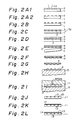
- the above optical disk 10 is manufactured through the following steps. First, a photoresist master disk having a photoresist layer 2 formed uniformly on the main surface of the glass disk 1, as shown in Fig. 2A1, is prepared and a latent image in tracks of spots corresponding to given information are formed in spiral form or concentrically on the photoresist layer 2 using the laser beam La in a laser cutting step.
- the exposed photoresist master disk is set in a developing device and developed to provide tracks of minute upheavals (hereinafter referred to as pits) corresponding to signals to be recorded, on the photoresist master disk.
- pits minute upheavals
- the photoresist layer 2 of the developing master disk is dried to be fixed on the glass disk 1, providing a dry master disk as shown in Fig. 2B.
- the subsequent silver sputtering step silver is sputtered on the photoresist layer 2 to form a silver conductive film 3 thereon, yielding a mastering master disk 3a having a layer-lamination structure, as shown in Fig. 2C.
- the information recorded surface having pits formed thereon is rendered conductive by sputtering metal on the pits-formed photoresist layer in the above manner.
- a nickel electroforming step the acquired mastering master disk is placed in a nickel electroforming tank to plate nickel (Ni) on the silver conductive film 3 to form a thick nickel layer 4 or nickel stamper, yielding a laminated structure of the nickel stamper and the glass disk, as shown in Fig. 2D.
- the nickel layer 4 or stamper is separated from the glass disk 1, as shown in Fig. 2E.
- the photoresist layer 2 remaining on the nickel layer 4 is removed in a photoresist removing step, yielding the structure shown in Fig. 2F.
- An alkali solution or an organic solvent available on the market is used in the photoresist separation.
- the silver conductive film 3 is removed from the nickel layer 4, and the peripheral portion of the resultant nickel layer 4 is subjected to trimming or the like, providing the nickel stamper as shown in Fig. 2G.
- the nickel stamper Before an injection molding step as a replica making step is executed, the nickel stamper is attached to a predetermined location of an injection molding machine 5, as shown in Fig. 2H. After closing the nickel stamper as shown in Fig. 2I, the injection molding machine 5 is activated to inject a transparent resin material, such as melted PMMA (polymethyl methacrylate) or PC (polycarbonate) on the nickel stamper, and the resultant structure is taken out after the resin material has been cured.
- a transparent resin material such as melted PMMA (polymethyl methacrylate) or PC (polycarbonate)
- the pits of the substrate 11 are formed deeper than those made by the prior art, and a liquid light-emitting material 13 including a phosphor, fluorescent member or the like is coated on the pits-formed surface (see Fig. 2J) by a spin coating method so that the material 13 is filled in the pits.
- the island-shaped light-emitting regions 13 serving as a light-emitting layer are formed in the pits on the substrate 11.
- the reflection layer 14 which contacts the light-emitting members 13 in the pits and the main surface of the substrate 11 are formed (see Fig. 2K), then the protective layer 15 is formed on the resultant structure (see Fig. 2L) by a well-known method, completing an optical disk.
- the spatial frequency up to 2NA(1/ ⁇ 1+1/ ⁇ 2) can be picked up using a special pickup in the apparatus as disclosed in Published Unexamined Japanese Patent No. Hei 2-50328 applied by the present applicant, where NA is the number of apertures of the objective lens for reading information, ⁇ 1 is the wavelength of light to be irradiated, and ⁇ 2 is the wavelength of light to be emitted from the light-emitting material in response to the irradiated light.
- the optical disk having the above structure can record information of a spatial frequency up to approximately twice the amount possible in the prior art, thus ensuring high-density recording on an optical disk.
- a method of manufacturing an optical disk on which light-emitting regions for absorbing a laser beam and emitting light of a wavelength different from that of the laser beam and reflection regions for reflecting a laser beam irradiated thereon are alternately arranged comprises the steps of forming a transparent substrate having a plurality of recesses arranged on a main surface thereof, filling a light-emitting member consisting of a fluorescent member in the recesses, and forming a reflection layer contacting the light-emitting member in the recesses and the main surface of the substrate. It is therefore possible to manufacture optical disks which can ensure recording/reproduction of information at high density.
Landscapes
- Engineering & Computer Science (AREA)
- Manufacturing & Machinery (AREA)
- Manufacturing Optical Record Carriers (AREA)
Applications Claiming Priority (2)
| Application Number | Priority Date | Filing Date | Title |
|---|---|---|---|
| JP145917/90 | 1990-06-04 | ||
| JP14591790A JPH0438733A (ja) | 1990-06-04 | 1990-06-04 | 光ディスク製造方法 |
Publications (2)
| Publication Number | Publication Date |
|---|---|
| EP0460346A2 true EP0460346A2 (fr) | 1991-12-11 |
| EP0460346A3 EP0460346A3 (en) | 1992-01-22 |
Family
ID=15396066
Family Applications (1)
| Application Number | Title | Priority Date | Filing Date |
|---|---|---|---|
| EP19910100475 Withdrawn EP0460346A3 (en) | 1990-06-04 | 1991-01-16 | Method of manufacturing optical disk |
Country Status (2)
| Country | Link |
|---|---|
| EP (1) | EP0460346A3 (fr) |
| JP (1) | JPH0438733A (fr) |
Cited By (5)
| Publication number | Priority date | Publication date | Assignee | Title |
|---|---|---|---|---|
| WO2000055850A1 (fr) * | 1999-03-16 | 2000-09-21 | Trid Store Ip, L.L.C. | Supports d'informations optiques multi-couches a lecture/enregistrement par fluorescence et procede de fabrication |
| US6589626B2 (en) | 2000-06-30 | 2003-07-08 | Verification Technologies, Inc. | Copy-protected optical media and method of manufacture thereof |
| DE4303937B4 (de) * | 1992-02-10 | 2006-08-17 | Mitsuboshi Belting Ltd., Kobe | V-Rippenriemen |
| US7124944B2 (en) | 2000-06-30 | 2006-10-24 | Verification Technologies, Inc. | Product packaging including digital data |
| US7303803B2 (en) | 2000-06-30 | 2007-12-04 | Verification Technologies, Inc. | Copy-protected optical media and method of manufacture thereof |
Families Citing this family (1)
| Publication number | Priority date | Publication date | Assignee | Title |
|---|---|---|---|---|
| KR100230244B1 (ko) * | 1995-01-24 | 1999-11-15 | 윤종용 | 다층 광 기록 매체의 제조방법 및 그 장치 |
Family Cites Families (1)
| Publication number | Priority date | Publication date | Assignee | Title |
|---|---|---|---|---|
| JP2904434B2 (ja) * | 1988-08-12 | 1999-06-14 | パイオニア株式会社 | 光学式情報記録媒体及びその再生装置 |
-
1990
- 1990-06-04 JP JP14591790A patent/JPH0438733A/ja active Pending
-
1991
- 1991-01-16 EP EP19910100475 patent/EP0460346A3/en not_active Withdrawn
Cited By (6)
| Publication number | Priority date | Publication date | Assignee | Title |
|---|---|---|---|---|
| DE4303937B4 (de) * | 1992-02-10 | 2006-08-17 | Mitsuboshi Belting Ltd., Kobe | V-Rippenriemen |
| WO2000055850A1 (fr) * | 1999-03-16 | 2000-09-21 | Trid Store Ip, L.L.C. | Supports d'informations optiques multi-couches a lecture/enregistrement par fluorescence et procede de fabrication |
| US6338935B1 (en) | 1999-03-16 | 2002-01-15 | Tridstore Ip Llc | Multi-layer optical information carriers with fluorescent reading/recording and method for their production |
| US6589626B2 (en) | 2000-06-30 | 2003-07-08 | Verification Technologies, Inc. | Copy-protected optical media and method of manufacture thereof |
| US7124944B2 (en) | 2000-06-30 | 2006-10-24 | Verification Technologies, Inc. | Product packaging including digital data |
| US7303803B2 (en) | 2000-06-30 | 2007-12-04 | Verification Technologies, Inc. | Copy-protected optical media and method of manufacture thereof |
Also Published As
| Publication number | Publication date |
|---|---|
| JPH0438733A (ja) | 1992-02-07 |
| EP0460346A3 (en) | 1992-01-22 |
Similar Documents
| Publication | Publication Date | Title |
|---|---|---|
| US5182669A (en) | High density optical disk and method of making | |
| US5843626A (en) | Method for manufacturing a master disc for optical discs | |
| EP0108258B1 (fr) | Disque matrice pour la fabrication d'un disque optique, méthode et système pour sa fabrication | |
| EP0414380A2 (fr) | Appareil d'enregistrement et de reproduction optique | |
| EP0992989A1 (fr) | Procédé pour la fabrication d'un support d'enregistrement optique | |
| EP0099085A1 (fr) | Disque optique | |
| EP0025253A1 (fr) | Disque d'enregistrement optique | |
| JP2007122875A (ja) | 光学的記憶媒体およびその製造方法 | |
| US4141731A (en) | Method of creating a replicating matrix | |
| US5096563A (en) | Method of manufacturing optical disk | |
| US3954469A (en) | Method of creating a replicating matrix | |
| US4877713A (en) | Preformatted optical recording card and method of producing the same | |
| EP0460346A2 (fr) | Méthode de fabrication d'un disque optique | |
| JP2977531B2 (ja) | 光ディスク用マスタディスク及びその製造方法 | |
| EP0460347B1 (fr) | Disque optique et sa méthode de fabrication | |
| US6190748B1 (en) | Optical discs | |
| KR100188922B1 (ko) | 광디스크 제조용 유리기판 및 포토마스크의 제조방법 | |
| NL8303194A (nl) | Registratiedrager van optisch leesbare data en werkwijze voor de vervaardiging daarvan. | |
| US6272101B1 (en) | Method and device for instantly encoding digitized information on a stamper from which compact discs can be made | |
| WO2004025641A1 (fr) | Procede de production d'un original d'utilisation de support d'enregistrement optique et procede de production d'un tel support | |
| JP3187067B2 (ja) | 光ディスク製造方法 | |
| WO1999004395A1 (fr) | Creation d'images graphiques sur un disque optique | |
| KR100686146B1 (ko) | 광 기록 매체 제조방법 | |
| KR20010109936A (ko) | 광 디스크의 씨아이 기록방법 | |
| AU744670B2 (en) | Optical recording medium and method of producing same |
Legal Events
| Date | Code | Title | Description |
|---|---|---|---|
| PUAI | Public reference made under article 153(3) epc to a published international application that has entered the european phase |
Free format text: ORIGINAL CODE: 0009012 |
|
| PUAL | Search report despatched |
Free format text: ORIGINAL CODE: 0009013 |
|
| AK | Designated contracting states |
Kind code of ref document: A2 Designated state(s): DE FR GB |
|
| AK | Designated contracting states |
Kind code of ref document: A3 Designated state(s): DE FR GB |
|
| 17P | Request for examination filed |
Effective date: 19920408 |
|
| 17Q | First examination report despatched |
Effective date: 19941004 |
|
| STAA | Information on the status of an ep patent application or granted ep patent |
Free format text: STATUS: THE APPLICATION IS DEEMED TO BE WITHDRAWN |
|
| 18D | Application deemed to be withdrawn |
Effective date: 19950215 |