EP0461309B1 - Datenübertragungsanordnung bestehend aus einer Haupteinrichtung angeschlossen an einer Mehrzahl von sekundären Einrichtungen - Google Patents
Datenübertragungsanordnung bestehend aus einer Haupteinrichtung angeschlossen an einer Mehrzahl von sekundären Einrichtungen Download PDFInfo
- Publication number
- EP0461309B1 EP0461309B1 EP90201197A EP90201197A EP0461309B1 EP 0461309 B1 EP0461309 B1 EP 0461309B1 EP 90201197 A EP90201197 A EP 90201197A EP 90201197 A EP90201197 A EP 90201197A EP 0461309 B1 EP0461309 B1 EP 0461309B1
- Authority
- EP
- European Patent Office
- Prior art keywords
- eslic1
- data
- secondary devices
- clock
- data transfer
- Prior art date
- Legal status (The legal status is an assumption and is not a legal conclusion. Google has not performed a legal analysis and makes no representation as to the accuracy of the status listed.)
- Expired - Lifetime
Links
- 230000003111 delayed effect Effects 0.000 description 2
- 239000000470 constituent Substances 0.000 description 1
- 238000001514 detection method Methods 0.000 description 1
Images


Classifications
-
- H—ELECTRICITY
- H04—ELECTRIC COMMUNICATION TECHNIQUE
- H04L—TRANSMISSION OF DIGITAL INFORMATION, e.g. TELEGRAPHIC COMMUNICATION
- H04L12/00—Data switching networks
- H04L12/28—Data switching networks characterised by path configuration, e.g. LAN [Local Area Networks] or WAN [Wide Area Networks]
- H04L12/40—Bus networks
- H04L12/407—Bus networks with decentralised control
- H04L12/413—Bus networks with decentralised control with random access, e.g. carrier-sense multiple-access with collision detection [CSMA-CD]
- H04L12/4135—Bus networks with decentralised control with random access, e.g. carrier-sense multiple-access with collision detection [CSMA-CD] using bit-wise arbitration
-
- H—ELECTRICITY
- H04—ELECTRIC COMMUNICATION TECHNIQUE
- H04L—TRANSMISSION OF DIGITAL INFORMATION, e.g. TELEGRAPHIC COMMUNICATION
- H04L12/00—Data switching networks
- H04L12/28—Data switching networks characterised by path configuration, e.g. LAN [Local Area Networks] or WAN [Wide Area Networks]
- H04L12/40—Bus networks
Definitions
- the present invention relates to a data transfer apparatus comprising a primary device connected to a plurality of secondary devices, the apparatus comprising for each secondary device one data link, one clock link and one read/write link.
- these three links constitute the minimum configuration of a data transfer connection so that in case the primary device has to be connected to a plurality of m x n secondary devices, the required data transfer connection has to comprise a total number of links equal to 3 x m x n, each set of 3 links being associated to a distinct secondary device.
- This total number of links may be slightly reduced by using all the clock links as well as all the read/write links of the m x n secondary devices in common. Indeed, as a result the primary device is then only connected to one clock link, one read/write link and as many data links as there are secondary devices so that the data transfer connection then comprises a total of 2 + (m x n) links, each data link being associated to a distinct secondary device.
- a drawback of such a connection is that when the primary device is integrated on an electronic chip the relative high number of links ( 3 x m x n or 2 + (m x n)) also requires an identical high number of pins and this is generally unacceptable.
- An object of the present invention is to provide a data transfer apparatus of the above type but requiring a relatively smaller number of links.
- this object is achieved due to the fact that said primary device is connected to m x n secondary devices, m being ⁇ 2, by one data link comprising m x n data channels assigned to respective ones of said secondary devices, by m clock links connected to m respective groups each of n secondary devices and carrying m clock signals having a same clock frequency and being mutually shifted by 1/m th of a cycle of said clock frequency, and by n read/write links connected to n respective groups each of m secondary devices and carrying n read/write signals mutually shifted by one cycle of said clock frequency, each of said secondary devices belonging to a distinct pair of one group out of said m groups and of one group out of said n groups.
- the present invention is based on the insight of assigning channels of a multiplex data link to respective secondary devices and of giving the m clock links and the n read/write links a double purpose: carrying the clock signal and the read/write signal respectively and by their combination allowing data transfer to the secondary devices over the allocated channels.
- Fig. 1 shows a portion of a digital communication exchange and more particularly a data transfer connection between a primary device constituted by an electronic chip DSP carrying 4 Digital Signal Processors (not shown) and 4 secondary devices constituted by respective Enhanced Subscriber Line Interface Circuits ESLIC1 to ESLIC4.
- This data transfer connection links the DSP to any of the 4 line interface circuits ESLIC1/4 by sets of three links:
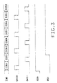
- the data link IOB of which the like named signal is shown in Fig. 3, is used to transfer frames of 16 bits of control data in each direction, i.e. from the DSP to the ESLIC's and vice versa, one bit being transferred per clock cycle.
- This control data is for instance constituted by off-hook or on-hook detection signals of a subscriber telephone set.
- this data link IOB may carry four multiplexed channels IOB1 to IOB4 (Fig. 3) which may then be assigned to respective ones of the four circuits ESLIC1/4 as well as to the four digital signal processors of the DSP chip.
- the assignment of the ESLIC1/4 is defined by the connections (Fig.1) and by the relative timing between the above read/write signals RD0/1 and clock signals GKC0/1 (Fig. 3) as explained below.
- the clock signal GKC1 (Fig. 3) is delayed or shifted by half a clock cycle with respect to the clock signal GKC0, whilst the read/write signal RD1 is delayed with respect to the other read/write signal RD0 by a full clock cycle of GKC0/1.
- Each line interface circuit ESLIC1/4 includes a divider circuit (not shown) which divides by two the clock signal applied at its terminal GKC0/1.
- the four ESLIC1-4 operate at a clock frequency of 256 kHz instead of the 512 kHz supplied at their clock input GKC0/1. This means that only one out of the two clock cycles of GKC0/1 is handled or acknowledged by ESLIC1/4.
- each line interface circuit ESLIC1/4 also includes a gating circuit (not shown) which enables data transfer from/to the data link IOB when both the other signals RD0/1 and GKC0/1 (one out of the two) applied thereto are activated or high.
- the read/write signals RD0-1 and the clock signals GKC0-1 are not only used separately for enabling the transfer of the control data IOB1-4 between the data link IOB and the line interface circuits ESLIC1-4, but are also used in combination for identifying and selecting the line interface circuit ESLIC1/4 associated to the control data IOB1/4 actually on the data link IOB. Because the data link IOB carries control data IOB1-4 which is subdivided into frames of 16 bits, the read/write signal RD0/1 remains active or high for 16 occurences of IOB1/4, i.e. for 32 clock cycles of GKC0/1.
- control data in channel IOB1 is transferred between the line interface circuit ESLIC1 and the data link IOB when both the read/write signal RD0 and, e.g., the odd occurences of the clock signal GKC0 are high.
- control data in channel IOB2 is on the data link IOB when both RD0 and the odd occurences of GKC1 are high
- control data in channel IOB3 is on the data link IOB when both RD1 and the even occurences of GKC0 are high
- control data in channel IOB4 is on the data link IOB when both RD1 and the even occurences of GKC1 are high.
- the above signals IOB, GKC0/1 and RD0/1 are generated at respectively like named outputs of a circuit shown in Fig. 4.
- a master clock signal GKC of 4,096 kHz and control data IOB1-4 of the four digital signal processors of the DSP and intended to like named channels of the data link IOB are applied to inputs of this circuit.
- this circuit forms part of the DSP and includes a multiplexer MUX, a binary counter BC, an inverter I0, two AND gates A0 and A1, and three D-flip flops FF0, FF1 and FF2.
- the master clock signal GKC is supplied to the multiplexer MUX as well as to the binary counter BC which subdivides the frequency of this signal GKC so as to provide, amongst others, signals of 1,024 kHz, 512 kHz and 8 kHz.
- the four control data IOB1-4 are also applied to the multiplexer MUX at one output of which the 4-channels multiplexed data IOB is generated, MUX generates also a frame synchronization signal FR which is applied to the binary counter BC in order to synchronize the above signals IOB, GKC0-1 and RD0-1.
- the outputs at 1,024 kHz and at 512 kHz of BC are connected to the two inputs of the AND gate A0 directly and via the inverter I0 respectively.
- the output of A0 and the master clock GKC are connected to the clock and D inputs of the D-flip flop FF0 respectively.
- the 512 kHz clock signal GKC0 is generated.
- the outputs at 1,024 kHz and at 512 kHz of BC are also directly connected to the two inputs of the AND gate A1 whose output is connected to the clock input of the D-flip flop FF1, the latter FF1 being also controlled by the master clock signal GKC applied to its D input.
- the 512 kHz clock signal GKC1 is available at the output of FF1.
- the output at 8 kHz of BC constitutes the read/write signal RD0 and is also connected to the input of the D-flip flop FF2.
- the D input of the D-flip flop FF2 is controlled by the signal at the output of the AND gate A0 and provides at its output the 8 kHz read/write signal RD1.
Landscapes
- Engineering & Computer Science (AREA)
- Computer Networks & Wireless Communication (AREA)
- Signal Processing (AREA)
- Communication Control (AREA)
- Time-Division Multiplex Systems (AREA)
- Information Transfer Systems (AREA)
- Small-Scale Networks (AREA)
Claims (8)
- Datenübertragungsvorrichtung, die ein primäres Gerät (DSP) umfaßt, das mit einer Vielzahl von sekundären Geräten (ESLIC1-4) verbunden ist, wobei die Vorrichtung für jedes sekundäre Gerät (ESLIC1/4) eine Datenübertragungsleitung (IOB), eine Taktübertragungsleitung (GKC0/1) und eine Schreib/Leseübertragungsleitung (RD0/1) umfaßt,
dadurch gekennzeichnet, daß das primäre Gerät (DSP) mit m x n sekundären Geräten (ESLIC1-4), wobei m ≧ 2 ist, durch eine Datenübertragungsleitung (IOB), die m x n Datenkanäle enthält, die den jeweiligen der sekundären Geräte (ESLIC1-4) zugeordnet sind, durch m Taktübertragungsleitungen (GKC0-1), die mit m entsprechenden Gruppen jeweils der n sekundären Geräte (ESLIC1-3; ESLIC2-4) verbunden sind, und die m Taktsignale übermittelt, welche eine gleiche Taktfrequenz haben und gegeneinander durch die 1/m-te eines Zyklus der Taktfrequenz verschoben sind, und durch n Schreib/Leseübertragungsleitungen (RD0-1) verbunden ist, die mit n entsprechenden Gruppen jeweils von m sekundären Geräten (ESLIC1-2; ESLIC3-4) verbunden sind und die n Schreib/Lesesignale übermitteln, die gegeneinander um einen Zyklus der Taktfrequenz verschoben sind, wobei jedes der sekundären Geräte (ESLIC1-4) zu einem bestimmten Paar aus einer Gruppe von den m Gruppen (ESLIC1-3; ESLIC2-4) und aus einer Gruppe vom der n Gruppen (ESLIC1-2; ESLIC3-4) gehört. - Datenübertragungsvorrichtung gemäß Anspruch 1, dadurch gekennzeichnet, daß die Vorrichtung dahingehend angepaßt ist, daß sie Daten zwischen dem primären Gerät (DSP) und einem sekundären Gerät (ESLIC1/4) überträgt, wenn sich sowohl das zugehörige Schreib/Lesesignal (RD0/1) wie das Taktsignal (GKC0/1) in einem vorgegebenen Status befinden.
- Datenübertragungsvorrichtung gemäß Anspruch 1, dadurch gekennzeichnet, daß die Taktfrequenz n Mal höher als die Frequenz ist, bei der die sekundären Geräte (ESLIC1-4) arbeiten.
- Datenübertragungsvorrichtung gemäß Anspruch 3, dadurch gekennzeichnet, daß die Taktfrequenz, bei der die m x n gemultiplexten Datenkanäle auf der Datenübertragungsleitung (IOB) übertragen werden, m Mal höher als die Taktfrequenz ist.
- Datenübertragungsvorrichtung gemäß den Ansprüchen 2 und 3, dadurch gekennzeichnet, daß die Vorrichtung so angepaßt ist, daß die Daten übertragen werden, wenn nur bei einem von n Vorkommen sich die beiden zugehörigen Schreib/Lesesignale (RD0/1) und Taktsignale (GKC0/1) im vorgegebenen Status befinden.
- Datenübertragungsvorrichtung gemäß Anspruch 1, dadurch gekennzeichnet, daß die Daten zwischen dem primären Gerät (DSP) und jedem der sekundären Geräte (ESLIC1/4) jeweils alle n Zyklen der Taktfrequenz übertragen werden.
- Datenübertragungsvorrichtung gemäß Anspruch 1, dadurch gekennzeichnet, daß das primäre Gerät (DSP) die Übertragung der Daten steuert.
- Datenübertragungsvorrichtung gemäß einem beliebigen der vorstehenden Ansprüche und wobei m gleich n ist.
Priority Applications (6)
| Application Number | Priority Date | Filing Date | Title |
|---|---|---|---|
| EP90201197A EP0461309B1 (de) | 1990-05-11 | 1990-05-11 | Datenübertragungsanordnung bestehend aus einer Haupteinrichtung angeschlossen an einer Mehrzahl von sekundären Einrichtungen |
| DE69021873T DE69021873T2 (de) | 1990-05-11 | 1990-05-11 | Datenübertragungsanordnung bestehend aus einer Haupteinrichtung angeschlossen an einer Mehrzahl von sekundären Einrichtungen. |
| CA002042298A CA2042298C (en) | 1990-05-11 | 1991-05-10 | Data transfer connection between a primary device and a plurality of secondary devices with a reduced number of links |
| AU76456/91A AU644161B2 (en) | 1990-05-11 | 1991-05-10 | Data transfer connection arrangement |
| US07/699,341 US5263023A (en) | 1990-05-11 | 1991-05-13 | Data transfer connection between a primary device and a plurality of secondary with a reduced number of links |
| JP3107468A JPH04230140A (ja) | 1990-05-11 | 1991-05-13 | 少ない数のリンクによる主デバイスと複数の従デバイスとの間のデータ転送接続装置 |
Applications Claiming Priority (1)
| Application Number | Priority Date | Filing Date | Title |
|---|---|---|---|
| EP90201197A EP0461309B1 (de) | 1990-05-11 | 1990-05-11 | Datenübertragungsanordnung bestehend aus einer Haupteinrichtung angeschlossen an einer Mehrzahl von sekundären Einrichtungen |
Publications (2)
| Publication Number | Publication Date |
|---|---|
| EP0461309A1 EP0461309A1 (de) | 1991-12-18 |
| EP0461309B1 true EP0461309B1 (de) | 1995-08-23 |
Family
ID=8205013
Family Applications (1)
| Application Number | Title | Priority Date | Filing Date |
|---|---|---|---|
| EP90201197A Expired - Lifetime EP0461309B1 (de) | 1990-05-11 | 1990-05-11 | Datenübertragungsanordnung bestehend aus einer Haupteinrichtung angeschlossen an einer Mehrzahl von sekundären Einrichtungen |
Country Status (6)
| Country | Link |
|---|---|
| US (1) | US5263023A (de) |
| EP (1) | EP0461309B1 (de) |
| JP (1) | JPH04230140A (de) |
| AU (1) | AU644161B2 (de) |
| CA (1) | CA2042298C (de) |
| DE (1) | DE69021873T2 (de) |
Families Citing this family (7)
| Publication number | Priority date | Publication date | Assignee | Title |
|---|---|---|---|---|
| US6104724A (en) * | 1993-09-20 | 2000-08-15 | Transwitch Corp. | Asynchronous data transfer and source traffic control system |
| JP3516684B2 (ja) * | 1993-09-20 | 2004-04-05 | トランスウィッチ・コーポレーション | 非同期データ伝送及びソース・トラフィック制御システム |
| US6205155B1 (en) | 1999-03-05 | 2001-03-20 | Transwitch Corp. | Apparatus and method for limiting data bursts in ATM switch utilizing shared bus |
| US7313151B2 (en) * | 2002-02-06 | 2007-12-25 | Transwitch Corporation | Extendible asynchronous and synchronous interface bus for broadband access |
| US7274657B2 (en) * | 2002-12-23 | 2007-09-25 | Transwitch Corporation | Methods and apparatus for providing redundancy in an asynchronous data transfer and source traffic control system |
| US7342885B2 (en) * | 2003-01-15 | 2008-03-11 | Transwitch Corporation | Method and apparatus for implementing a backpressure mechanism in an asynchronous data transfer and source traffic control system |
| US7430201B1 (en) | 2003-03-21 | 2008-09-30 | Transwitch Corporation | Methods and apparatus for accessing full bandwidth in an asynchronous data transfer and source traffic control system |
Family Cites Families (8)
| Publication number | Priority date | Publication date | Assignee | Title |
|---|---|---|---|---|
| US3916108A (en) * | 1973-11-09 | 1975-10-28 | Multiplex Communicat Inc | Tdm communication system with centralized time slot address distribution |
| US4010326A (en) * | 1973-11-09 | 1977-03-01 | Multiplex Communications, Inc. | Line selective time division communication system |
| US3993870A (en) * | 1973-11-09 | 1976-11-23 | Multiplex Communications, Inc. | Time multiplex system with separate data, sync and supervision busses |
| US3919483A (en) * | 1973-12-26 | 1975-11-11 | Ibm | Parallel multiplexed loop interface for data transfer and control between data processing systems and subsystems |
| US4320502A (en) * | 1978-02-22 | 1982-03-16 | International Business Machines Corp. | Distributed priority resolution system |
| JPS5843767B2 (ja) * | 1978-07-10 | 1983-09-29 | 富士通株式会社 | 共通信号母線方式 |
| AU544150B2 (en) * | 1981-12-17 | 1985-05-16 | Xitel Pty Limited | A distributed control communications system |
| JPS6022335A (ja) * | 1983-07-19 | 1985-02-04 | Toshiba Corp | 半導体装置の製造方法 |
-
1990
- 1990-05-11 DE DE69021873T patent/DE69021873T2/de not_active Expired - Fee Related
- 1990-05-11 EP EP90201197A patent/EP0461309B1/de not_active Expired - Lifetime
-
1991
- 1991-05-10 CA CA002042298A patent/CA2042298C/en not_active Expired - Fee Related
- 1991-05-10 AU AU76456/91A patent/AU644161B2/en not_active Ceased
- 1991-05-13 US US07/699,341 patent/US5263023A/en not_active Expired - Fee Related
- 1991-05-13 JP JP3107468A patent/JPH04230140A/ja active Pending
Also Published As
| Publication number | Publication date |
|---|---|
| JPH04230140A (ja) | 1992-08-19 |
| US5263023A (en) | 1993-11-16 |
| AU644161B2 (en) | 1993-12-02 |
| DE69021873D1 (de) | 1995-09-28 |
| AU7645691A (en) | 1991-11-14 |
| CA2042298C (en) | 1998-06-16 |
| EP0461309A1 (de) | 1991-12-18 |
| CA2042298A1 (en) | 1991-11-12 |
| DE69021873T2 (de) | 1996-04-04 |
Similar Documents
| Publication | Publication Date | Title |
|---|---|---|
| EP0273249A2 (de) | Fehlertolerantes Koppelfeld mit wählbaren Betriebsarten | |
| US4916690A (en) | Division multiplex packet switching circuit using a circular shift register | |
| US5046067A (en) | Digital transmission system | |
| US3890469A (en) | Time division switching system | |
| EP0206641A2 (de) | Fernmeldezentralen | |
| US5878039A (en) | Bus rate adaptation and time slot assignment circuit for a sonet multiplex system | |
| US4804956A (en) | Rearrangeable digital signal space division switching system | |
| US4429391A (en) | Fault and error detection arrangement | |
| EP0461309A1 (de) | Datenübertragungsanordnung bestehend aus einer Haupteinrichtung angeschlossen an einer Mehrzahl von sekundären Einrichtungen | |
| CA1228928A (en) | Data rate conversion and supervisory bit insertion in a data system | |
| US5612954A (en) | Time switch system | |
| US4680759A (en) | Standard/proportional multiplexer | |
| US4160126A (en) | Modular multiplex/demultiplex apparatus | |
| US6049571A (en) | Encoding circuit with a function of zero continuous-suppression in a data transmission system | |
| US4160876A (en) | Modular multiplex/demultiplex apparatus | |
| JPS6320931A (ja) | デ−タ伝送装置 | |
| AU627751B2 (en) | Multi-channel controller DO NOT SEAL CASE WITHDRAWN | |
| KR900001028Y1 (ko) | 펄스부호 변조 다중장치의 동기패턴 삽입회로 | |
| JP3072494B2 (ja) | 並列形フレーム同期回路のチャネル選択状態のモニタ回路 | |
| GB2164821A (en) | Digital tie line | |
| JP2692476B2 (ja) | フレーム同期システム | |
| JP2521957B2 (ja) | 伝送システム | |
| KR100210780B1 (ko) | 프로세서와 디바이스간의 타임 슬롯 스위치의 데이터 정합회로 | |
| KR100447397B1 (ko) | 통신시스템의 비트에러방지장치 | |
| KR950006602B1 (ko) | 동기식 에드-드롭 전송장치 |
Legal Events
| Date | Code | Title | Description |
|---|---|---|---|
| PUAI | Public reference made under article 153(3) epc to a published international application that has entered the european phase |
Free format text: ORIGINAL CODE: 0009012 |
|
| AK | Designated contracting states |
Kind code of ref document: A1 Designated state(s): BE CH DE FR GB IT LI NL SE |
|
| 17P | Request for examination filed |
Effective date: 19920603 |
|
| 17Q | First examination report despatched |
Effective date: 19940314 |
|
| RAP1 | Party data changed (applicant data changed or rights of an application transferred) |
Owner name: ALCATEL N.V. Owner name: BELL TELEPHONE MANUFACTURING COMPANY NAAMLOZE VENN |
|
| GRAA | (expected) grant |
Free format text: ORIGINAL CODE: 0009210 |
|
| AK | Designated contracting states |
Kind code of ref document: B1 Designated state(s): BE CH DE FR GB IT LI NL SE |
|
| REF | Corresponds to: |
Ref document number: 69021873 Country of ref document: DE Date of ref document: 19950928 |
|
| ITF | It: translation for a ep patent filed | ||
| ET | Fr: translation filed | ||
| RAP2 | Party data changed (patent owner data changed or rights of a patent transferred) |
Owner name: ALCATEL N.V. Owner name: ALCATEL BELL NAAMLOZE VENNOOTSCHAP |
|
| PLBE | No opposition filed within time limit |
Free format text: ORIGINAL CODE: 0009261 |
|
| STAA | Information on the status of an ep patent application or granted ep patent |
Free format text: STATUS: NO OPPOSITION FILED WITHIN TIME LIMIT |
|
| NLT2 | Nl: modifications (of names), taken from the european patent patent bulletin |
Owner name: ALCATEL N.V. |
|
| 26N | No opposition filed | ||
| PGFP | Annual fee paid to national office [announced via postgrant information from national office to epo] |
Ref country code: GB Payment date: 19980414 Year of fee payment: 9 |
|
| PGFP | Annual fee paid to national office [announced via postgrant information from national office to epo] |
Ref country code: FR Payment date: 19980417 Year of fee payment: 9 |
|
| PGFP | Annual fee paid to national office [announced via postgrant information from national office to epo] |
Ref country code: DE Payment date: 19980420 Year of fee payment: 9 |
|
| PGFP | Annual fee paid to national office [announced via postgrant information from national office to epo] |
Ref country code: SE Payment date: 19980423 Year of fee payment: 9 |
|
| PGFP | Annual fee paid to national office [announced via postgrant information from national office to epo] |
Ref country code: BE Payment date: 19980427 Year of fee payment: 9 |
|
| PGFP | Annual fee paid to national office [announced via postgrant information from national office to epo] |
Ref country code: NL Payment date: 19980430 Year of fee payment: 9 Ref country code: CH Payment date: 19980430 Year of fee payment: 9 |
|
| PG25 | Lapsed in a contracting state [announced via postgrant information from national office to epo] |
Ref country code: GB Free format text: LAPSE BECAUSE OF NON-PAYMENT OF DUE FEES Effective date: 19990511 |
|
| PG25 | Lapsed in a contracting state [announced via postgrant information from national office to epo] |
Ref country code: SE Free format text: LAPSE BECAUSE OF NON-PAYMENT OF DUE FEES Effective date: 19990512 |
|
| PG25 | Lapsed in a contracting state [announced via postgrant information from national office to epo] |
Ref country code: LI Free format text: LAPSE BECAUSE OF NON-PAYMENT OF DUE FEES Effective date: 19990531 Ref country code: CH Free format text: LAPSE BECAUSE OF NON-PAYMENT OF DUE FEES Effective date: 19990531 Ref country code: BE Free format text: LAPSE BECAUSE OF NON-PAYMENT OF DUE FEES Effective date: 19990531 |
|
| BERE | Be: lapsed |
Owner name: ALCATEL BELL Effective date: 19990531 |
|
| PG25 | Lapsed in a contracting state [announced via postgrant information from national office to epo] |
Ref country code: NL Free format text: LAPSE BECAUSE OF NON-PAYMENT OF DUE FEES Effective date: 19991201 |
|
| GBPC | Gb: european patent ceased through non-payment of renewal fee |
Effective date: 19990511 |
|
| REG | Reference to a national code |
Ref country code: CH Ref legal event code: PL |
|
| EUG | Se: european patent has lapsed |
Ref document number: 90201197.2 |
|
| PG25 | Lapsed in a contracting state [announced via postgrant information from national office to epo] |
Ref country code: FR Free format text: LAPSE BECAUSE OF NON-PAYMENT OF DUE FEES Effective date: 20000131 |
|
| NLV4 | Nl: lapsed or anulled due to non-payment of the annual fee |
Effective date: 19991201 |
|
| PG25 | Lapsed in a contracting state [announced via postgrant information from national office to epo] |
Ref country code: DE Free format text: LAPSE BECAUSE OF NON-PAYMENT OF DUE FEES Effective date: 20000301 |
|
| REG | Reference to a national code |
Ref country code: FR Ref legal event code: ST |
|
| PG25 | Lapsed in a contracting state [announced via postgrant information from national office to epo] |
Ref country code: IT Free format text: LAPSE BECAUSE OF NON-PAYMENT OF DUE FEES;WARNING: LAPSES OF ITALIAN PATENTS WITH EFFECTIVE DATE BEFORE 2007 MAY HAVE OCCURRED AT ANY TIME BEFORE 2007. THE CORRECT EFFECTIVE DATE MAY BE DIFFERENT FROM THE ONE RECORDED. Effective date: 20050511 |