EP0461702B1 - Assemblage pour contact - Google Patents
Assemblage pour contact Download PDFInfo
- Publication number
- EP0461702B1 EP0461702B1 EP91201354A EP91201354A EP0461702B1 EP 0461702 B1 EP0461702 B1 EP 0461702B1 EP 91201354 A EP91201354 A EP 91201354A EP 91201354 A EP91201354 A EP 91201354A EP 0461702 B1 EP0461702 B1 EP 0461702B1
- Authority
- EP
- European Patent Office
- Prior art keywords
- contact
- support
- signal
- edge
- intermediate layer
- Prior art date
- Legal status (The legal status is an assumption and is not a legal conclusion. Google has not performed a legal analysis and makes no representation as to the accuracy of the status listed.)
- Expired - Lifetime
Links
Images

Classifications
-
- H—ELECTRICITY
- H05—ELECTRIC TECHNIQUES NOT OTHERWISE PROVIDED FOR
- H05K—PRINTED CIRCUITS; CASINGS OR CONSTRUCTIONAL DETAILS OF ELECTRIC APPARATUS; MANUFACTURE OF ASSEMBLAGES OF ELECTRICAL COMPONENTS
- H05K1/00—Printed circuits
- H05K1/02—Details
- H05K1/11—Printed elements for providing electric connections to or between printed circuits
- H05K1/118—Printed elements for providing electric connections to or between printed circuits specially for flexible printed circuits, e.g. using folded portions
-
- H—ELECTRICITY
- H01—ELECTRIC ELEMENTS
- H01R—ELECTRICALLY-CONDUCTIVE CONNECTIONS; STRUCTURAL ASSOCIATIONS OF A PLURALITY OF MUTUALLY-INSULATED ELECTRICAL CONNECTING ELEMENTS; COUPLING DEVICES; CURRENT COLLECTORS
- H01R12/00—Structural associations of a plurality of mutually-insulated electrical connecting elements, specially adapted for printed circuits, e.g. printed circuit boards [PCB], flat or ribbon cables, or like generally planar structures, e.g. terminal strips, terminal blocks; Coupling devices specially adapted for printed circuits, flat or ribbon cables, or like generally planar structures; Terminals specially adapted for contact with, or insertion into, printed circuits, flat or ribbon cables, or like generally planar structures
- H01R12/70—Coupling devices
- H01R12/71—Coupling devices for rigid printing circuits or like structures
- H01R12/72—Coupling devices for rigid printing circuits or like structures coupling with the edge of the rigid printed circuits or like structures
- H01R12/721—Coupling devices for rigid printing circuits or like structures coupling with the edge of the rigid printed circuits or like structures cooperating directly with the edge of the rigid printed circuits
-
- H—ELECTRICITY
- H01—ELECTRIC ELEMENTS
- H01R—ELECTRICALLY-CONDUCTIVE CONNECTIONS; STRUCTURAL ASSOCIATIONS OF A PLURALITY OF MUTUALLY-INSULATED ELECTRICAL CONNECTING ELEMENTS; COUPLING DEVICES; CURRENT COLLECTORS
- H01R12/00—Structural associations of a plurality of mutually-insulated electrical connecting elements, specially adapted for printed circuits, e.g. printed circuit boards [PCB], flat or ribbon cables, or like generally planar structures, e.g. terminal strips, terminal blocks; Coupling devices specially adapted for printed circuits, flat or ribbon cables, or like generally planar structures; Terminals specially adapted for contact with, or insertion into, printed circuits, flat or ribbon cables, or like generally planar structures
- H01R12/70—Coupling devices
- H01R12/71—Coupling devices for rigid printing circuits or like structures
- H01R12/72—Coupling devices for rigid printing circuits or like structures coupling with the edge of the rigid printed circuits or like structures
- H01R12/73—Coupling devices for rigid printing circuits or like structures coupling with the edge of the rigid printed circuits or like structures connecting to other rigid printed circuits or like structures
- H01R12/735—Printed circuits including an angle between each other
- H01R12/737—Printed circuits being substantially perpendicular to each other
-
- H—ELECTRICITY
- H01—ELECTRIC ELEMENTS
- H01R—ELECTRICALLY-CONDUCTIVE CONNECTIONS; STRUCTURAL ASSOCIATIONS OF A PLURALITY OF MUTUALLY-INSULATED ELECTRICAL CONNECTING ELEMENTS; COUPLING DEVICES; CURRENT COLLECTORS
- H01R13/00—Details of coupling devices of the kinds covered by groups H01R12/70 or H01R24/00 - H01R33/00
- H01R13/02—Contact members
- H01R13/03—Contact members characterised by the material, e.g. plating, or coating materials
-
- H—ELECTRICITY
- H05—ELECTRIC TECHNIQUES NOT OTHERWISE PROVIDED FOR
- H05K—PRINTED CIRCUITS; CASINGS OR CONSTRUCTIONAL DETAILS OF ELECTRIC APPARATUS; MANUFACTURE OF ASSEMBLAGES OF ELECTRICAL COMPONENTS
- H05K1/00—Printed circuits
- H05K1/02—Details
- H05K1/03—Use of materials for the substrate
- H05K1/05—Insulated conductive substrates, e.g. insulated metal substrate
-
- H—ELECTRICITY
- H05—ELECTRIC TECHNIQUES NOT OTHERWISE PROVIDED FOR
- H05K—PRINTED CIRCUITS; CASINGS OR CONSTRUCTIONAL DETAILS OF ELECTRIC APPARATUS; MANUFACTURE OF ASSEMBLAGES OF ELECTRICAL COMPONENTS
- H05K2201/00—Indexing scheme relating to printed circuits covered by H05K1/00
- H05K2201/03—Conductive materials
- H05K2201/0302—Properties and characteristics in general
- H05K2201/0311—Metallic part with specific elastic properties, e.g. bent piece of metal as electrical contact
-
- H—ELECTRICITY
- H05—ELECTRIC TECHNIQUES NOT OTHERWISE PROVIDED FOR
- H05K—PRINTED CIRCUITS; CASINGS OR CONSTRUCTIONAL DETAILS OF ELECTRIC APPARATUS; MANUFACTURE OF ASSEMBLAGES OF ELECTRICAL COMPONENTS
- H05K2201/00—Indexing scheme relating to printed circuits covered by H05K1/00
- H05K2201/04—Assemblies of printed circuits
- H05K2201/044—Details of backplane or midplane for mounting orthogonal PCBs
-
- H—ELECTRICITY
- H05—ELECTRIC TECHNIQUES NOT OTHERWISE PROVIDED FOR
- H05K—PRINTED CIRCUITS; CASINGS OR CONSTRUCTIONAL DETAILS OF ELECTRIC APPARATUS; MANUFACTURE OF ASSEMBLAGES OF ELECTRICAL COMPONENTS
- H05K2201/00—Indexing scheme relating to printed circuits covered by H05K1/00
- H05K2201/09—Shape and layout
- H05K2201/09145—Edge details
- H05K2201/09172—Notches between edge pads
-
- H—ELECTRICITY
- H05—ELECTRIC TECHNIQUES NOT OTHERWISE PROVIDED FOR
- H05K—PRINTED CIRCUITS; CASINGS OR CONSTRUCTIONAL DETAILS OF ELECTRIC APPARATUS; MANUFACTURE OF ASSEMBLAGES OF ELECTRICAL COMPONENTS
- H05K2203/00—Indexing scheme relating to apparatus or processes for manufacturing printed circuits covered by H05K3/00
- H05K2203/30—Details of processes not otherwise provided for in H05K2203/01 - H05K2203/17
- H05K2203/302—Bending a rigid substrate; Breaking rigid substrates by bending
-
- H—ELECTRICITY
- H05—ELECTRIC TECHNIQUES NOT OTHERWISE PROVIDED FOR
- H05K—PRINTED CIRCUITS; CASINGS OR CONSTRUCTIONAL DETAILS OF ELECTRIC APPARATUS; MANUFACTURE OF ASSEMBLAGES OF ELECTRICAL COMPONENTS
- H05K3/00—Apparatus or processes for manufacturing printed circuits
- H05K3/0058—Laminating printed circuit boards onto other substrates, e.g. metallic substrates
-
- H—ELECTRICITY
- H05—ELECTRIC TECHNIQUES NOT OTHERWISE PROVIDED FOR
- H05K—PRINTED CIRCUITS; CASINGS OR CONSTRUCTIONAL DETAILS OF ELECTRIC APPARATUS; MANUFACTURE OF ASSEMBLAGES OF ELECTRICAL COMPONENTS
- H05K3/00—Apparatus or processes for manufacturing printed circuits
- H05K3/30—Assembling printed circuits with electric components, e.g. with resistors
- H05K3/32—Assembling printed circuits with electric components, e.g. with resistors electrically connecting electric components or wires to printed circuits
- H05K3/34—Assembling printed circuits with electric components, e.g. with resistors electrically connecting electric components or wires to printed circuits by soldering
- H05K3/3447—Lead-in-hole components
-
- H—ELECTRICITY
- H05—ELECTRIC TECHNIQUES NOT OTHERWISE PROVIDED FOR
- H05K—PRINTED CIRCUITS; CASINGS OR CONSTRUCTIONAL DETAILS OF ELECTRIC APPARATUS; MANUFACTURE OF ASSEMBLAGES OF ELECTRICAL COMPONENTS
- H05K3/00—Apparatus or processes for manufacturing printed circuits
- H05K3/36—Assembling printed circuits with other printed circuits
- H05K3/361—Assembling flexible printed circuits with other printed circuits
- H05K3/365—Assembling flexible printed circuits with other printed circuits by abutting, i.e. without alloying process
Definitions
- the invention relates to a contact assembly, in particular for use in a connector or the like, comprising at least one signal contact and at least one ground contact.
- Such contact assemblies are generally mounted in the housing of a connector element, wherein the contacts are made as a male or a female contact.
- attention has mainly been paid to the mechanical aspects of the connector assembly equiped with said contacts, in particular with respect to the forces required for coupling and decoupling the connector elements. Attention was only paid to the electrical aspects in that one aimed at realizing good reliable connections between the contacts of both connector elements.
- the electrical performance of the contacts as a circuit element becomes important.
- problems occur with higher signal speeds with respect to cross-over between signal contacts, transmission losses, reflections and ground bounce or switching noise. Up to the present it is attempted to obviate these problems by mounting the signal and ground contacts in a suitable distribution in the connector elements, wherein however these problems cannot be eliminated below rise times of 0.6 ns.
- European patent application 91200396 (published as EP-A-0 446 980) of the same applicant discloses a connector assembly, wherein these problems are obviated in that outer signal conductors connected to ground are provided, each of said outer signal conductors enclosing one or more signal contacts. Although said problems are eliminated in an effective manner by this connector assembly, the number of signal connections per unit surface in this connector assembly is restricted.
- the invention aims to provide an improved contact assembly of this type, wherein said problems which may occur at high speeds when used in a connector, can be eliminated by such a construction of the contact assembly itself that the performance of each signal contact as a circuit element can be predetermined and said signal distortions can be minimized, whereas moreover the number of signal connections per unit surface can be significantly increased.
- the contact assembly of the invention is characterised by the characterising features of claim 1.
- a contact assembly wherein a signal conductor with the opposite support part separated from said signal conductor by the intermediate layer, forms a transmission line, wherein a desired impedance of 50 or 75 ohm, for example, can be obtained by a suitable choise of the thickness of the insulating intermediate layer and the width of the signal conductor.
- a desired impedance of 50 or 75 ohm for example, can be obtained by a suitable choise of the thickness of the insulating intermediate layer and the width of the signal conductor.
- the mechanical and electrical functions of the signal contacts are separated in the contact assembly according to the invention, wherein the support performs the mechanical functions for the signal contacts and operates further as ground contact.
- the signal conductors operating as signal contacts can be designed for optimal signal transmission properties, wherein it is not necessary to take the mechanical properties into account. Thereby an excellent signal integrity can be guaranteed, because the signal contacts have a controlled impedance and moreover a low capacity and low inductance.
- the contact assembly according to the invention has the important advantage that a connector with a high density of signal contacts can be manufactured, because actually all contacts are signal contacts and no space is occupied by separate ground contacts. The manufacturing costs of the contact assembly according to the invention are relatively low, because a tooling change is not required to obtain contacts with different electrical properties or a different pattern of ground and signal connections.
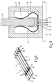
- Fig. 1 is a perspective view of a contact assembly in a flat position, wherein the pattern of signal conductors and contact pads can be seen.
- Fig. 2 schematically shows the use of the contact assembly of fig. 1 in a connector element.
- Fig. 3 is a perspective view of a further embodiment of a contact assembly.
- Fig. 4 schematically shows the use of the contact assembly of fig. 3 in a connector element.
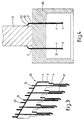
- Fig. 5 and 6 schematically show a perspective view and a side view, respectively, of two different embodiments of the contact assembly according to the invention.
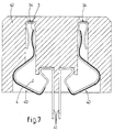
- Fig. 7 schematically shows the use of a variant of the contact assembly of fig. 6 in a connector element.
- Fig. 1 shows a contact assembly 1 comprising a strip-like support 2 and an insulating intermediate layer 3, upon which signal conductors 4 and contact pads 5 and 6 are provided.
- Fig. 1 shows the support 2 in perspective in a flat position
- fig. 2 shows the contact assembly 1 as applied in a connector element 7 of the so-called direct edge type, wherein the support 2 has been given a desired shape for contacting an edge of a printed circuit board.
- Slits 8 are provided at the opposite longitudinal edges of the strip-like support 2, whereby fingers 9 are obtained each carrying a contact pad 5 and a contact pad 6.
- each contact pad is provided with a contact button 10, wherein the strip-like support 2 is shaped in such a manner that the contact pads 5, 6 with the contact buttons 10 protrude so that as used in the connector element 7 the contact buttons 10 can contact corresponding contact pads of a printed circuit board 11 inserted into the connector element 7.
- the contact pads 5 are connected with the signal conductors 4.
- the contact pads 6 are connected with the support 2 through a conductive plating of a hole indicated by a circle.
- the contact pads 5 form signal contact pads, while the contact pads 6 form ground contact pads.
- the signal conductors 4 are connected with contact pins 12 substantially in the centre part of the support 2, which contact pins 12 project through openings 13 formed in the support 2 without contacting the material of the support 2.
- Ground contact pins 14 connected with the support 2 are provided between signal contact pins 12 of the signal conductors 4 successive in the longitudinal direction of the support 2.
- the contact pins 12, 14 are inserted in plated through holes of a printed circuit board 15 and are connected with the circuit paths of this printed circuit board 15 in this manner.
- the support 2 consists of a resilient conductive material, for example beryllium-copper which provides the mechanical strength and resilience for the signal conductors 4.
- the signal conductors 4 and the contact pads 5, 6 are made from a conductive layer, for example copper, which is provided on the insulating intermediate layer 3.
- Fig. 3 shows a contact assembly 29 to be used in a so-called indirect connector 30 as shown in fig. 4.
- the contact assembly 29 comprises a support 2 with an insulating intermediate layer 3 having contact pads 19, 20 on one longitudinal edge provided in the manner as shown in fig. 4.
- These contact pads 19, 20 are connected with corresponding contact pads of a printed circuit board 31 by soldering.
- the contact pads 19 and/or 20 can be made as contact springs in for connection to the contact pads of the printed circuit board 31.
- At the opposite side male contacts 32 are made out of the support 2, wherein the signal conductors 4 extend from the contact pads 19 upto adjacent the end of the contact pins 32.
- Fig. 5 shows in perspective a contact assembly 33 according to the invention which is provided with a female contact element 34 adapted to cooperate with a contact pin 32 of the contact assembly 29.
- Each contact assembly 33 comprises a support 2 partially coated with an insulating intermediate layer 3, on which a signal conductor 4 is formed.
- a contact pin 35 for connection to a printed circuit board not shown is formed out of the support 2 at one longitudinal edge.
- a contact pin 36 is provided which is connected with the signal conductor 4 by welding or the like and which extends through an opening formed in the support 2 without contacting the support 2.
- a contact pad 5 is provided on the intermediate layer 3.
- the edge of the support 2 without the intermediate layer 3 is bent along 180° back towards the insulating intermediate layer 3 in such a manner that a mainly u-shaped edge 34 is obtained.
- the web 37 of the u-shaped edge 34 is provided with an opening for the passage of a contact pin 32, wherein the signal conductor 4 of the contact pin 32 will contact the contact pad 5 and the material of the support 2 will contact the free leg 38 of the u-shaped edge 34.
- Fig. 6 shows an alternative contact assembly 39 according to the invention to be used in combination with the contact assembly 29.
- the contact assembly 39 is provided with a u-shaped edge 34 in the same manner as the contact assembly 33.
- At the other longitudinal edge of the support 2 there are however provided contact pads 5, 6 on the insulating intermediate layer 3 in the same manner as in the contact assembly according to figs. 1 and 2 instead of contact pins, which contact pads 5, 6 are not visible in fig. 6 and which are connected with the signal conductors 4 and the support 2, respectively.
- Fig. 7 shows a contact assembly 40 according to the invention corresponding with the same of fig. 6, wherein in this case contact pins 41 for connection to a printed circuit board are formed out of the edge opposite of the u-shaped edge 34.
- the insulating layer 3 only has signal contact pads 5 in this case, which contact pads 5 are connected with the signal conductors 4.
- Fig. 7 further shows a suitable housing 42 for the contact assembly 40.
- this embodiment has the advantage that the contact pins 41 also provide the required contact pressure for the contact pads 5.
- contact assemblies 33, 39 shown in figs. 5 and 6 can be made as a strip of contact assemblies.
- each signal conductor 4 with the opposite part of the support 2 separated from the same by the intermediate layer 3 forms a transmission line, wherein a desired impedance can be obtained by a suitable choice of the thickness of the insulating layer 3 and the width of the signal conductor 4.
- a thickness including any adhesive of 50 micron and a width of the signal conductor 4 of 200 micron results in an impedance of approximately 50 ohm.
- the support 2 consisting of a resilient conductive material can be designed for optimum mechanical characteristics and the signal conductors 4 can be designed for optimum characteristics for signal transmission.
- An excellent signal integrity for the contacts of the contact assembly according to the invention is guaranteed because the contacts besides a controlled impedance further have a low capacity and low inductance.
- a connector equipped with the contact assembly according to the invention can have a high density of signal contacts because actually all contacts are signal contacts.
- the manufacturing costs of the contact assembly according to the invention are relatively low because a tooling change is not required to obtain contacts with different electrical properties.
- the signal conductors and contact pads can be formed in any desired pattern of the support 2.
- contact pins for connection to a printed circuit board can be provided with a press-fit portion in a usual manner.
Landscapes
- Engineering & Computer Science (AREA)
- Microelectronics & Electronic Packaging (AREA)
- Coupling Device And Connection With Printed Circuit (AREA)
- Auxiliary Devices For And Details Of Packaging Control (AREA)
- Inert Electrodes (AREA)
- Details Of Connecting Devices For Male And Female Coupling (AREA)
Claims (6)
- Ensemble de contacts (33, 39, 40) ayant au moins un contact pour signaux et au moins un contact de mise à la terre, en particulier pour utilisation dans un raccord ou analogue, comportant un support (2) en matériau conducteur élastique, une couche intermédiaire isolante (3) agencée sur le support et au moins un conducteur de signaux (4) supporté par la couche intermédiaire isolante, dans lequel le support (2) est utilisé en tant que conducteur de mise à la terre, dans lequel deux ou plusieurs patins de contact adjacents (5, 38) sont agencés pour chaque conducteur de signaux ou chaque groupe de conducteurs de signaux adjacents à un premier bord du support, dans lequel un premier patin de contact (38) est relié au support et l'autre patin, ou les autres patins de contact (5) est relié ou sont reliés aux conducteurs de signaux respectifs (4), caractérisé en ce que le support (2) a une partie faisant saillie (38) au niveau d'un premier côté incurvé de 180° vers ladite couche intermédiaire (3) d'une manière telle qu'un bord (34) ayant en coupe une forme à peu près en U soit obtenu, dans lequel pour chaque conducteur de signaux (4) un patin de contact (5) est agencé sur la couche intermédiaire (3) opposée à la patte libre (38) du bord en forme de U, ladite patte libre fournissant au support ledit patin de contact.
- Ensemble de contacts selon la revendication 1, caractérisé en ce qu'au niveau d'un second bord du support (2) pour chaque conducteur de signaux (4) ou chaque groupe de conducteurs de signaux (4) des patins de contact (5, 6) destinés au support et le conducteur ou les conducteurs de signaux correspondants, de manière respective, sont fournis pour être connectés aux patins de contact correspondants d'une carte à circuits imprimés.
- Ensemble de contacts selon la revendication 1 ou 2, caractérisé en ce que le support (2) est courbé au niveau de l'emplacement des patins de contact (5, 6) d'une manière telle que lesdits patins de contact font saillie pour être en contact avec les patins de contact correspondants d'une carte à circuits imprimés ou avec un contact complémentaire, respectivement.
- Ensemble de contacts selon l'une quelconque des revendications précédentes, caractérisé en ce que la patte libre (38) du bord en forme de U (34) est dirigée vers le bord opposé du support (2), une ouverture étant agencée dans l'âme (37) du bord en forme de U pour l'insertion d'un doigt de contact (32) adapté pour être en contact avec la patte libre (38) du bord en forme de U sur le premier côté et le ou les patins de contact correspondants (5) sur l'autre côté.
- Ensemble de contacts selon l'une quelconque des revendications précédentes, caractérisé en ce que ledit bord en forme de U (34) est divisé en doigts par des fentes, chacun étant associé à au moins un conducteur de signaux (4).
- Ensemble de contacts selon l'une quelconque des revendications précédentes, caractérisé en ce que le support (2), au niveau de son côté opposé au bord en forme de U (34), a un bord faisant saillie librement au delà de la couche intermédiaire isolante (3) et divisé en doigts de contact (35) destinés à être connectés à une carte à circuits imprimés.
Applications Claiming Priority (2)
| Application Number | Priority Date | Filing Date | Title |
|---|---|---|---|
| NL9001347 | 1990-06-14 | ||
| NL9001347A NL9001347A (nl) | 1990-06-14 | 1990-06-14 | Contactsamenstel. |
Publications (2)
| Publication Number | Publication Date |
|---|---|
| EP0461702A1 EP0461702A1 (fr) | 1991-12-18 |
| EP0461702B1 true EP0461702B1 (fr) | 1995-08-30 |
Family
ID=19857242
Family Applications (1)
| Application Number | Title | Priority Date | Filing Date |
|---|---|---|---|
| EP91201354A Expired - Lifetime EP0461702B1 (fr) | 1990-06-14 | 1991-06-04 | Assemblage pour contact |
Country Status (7)
| Country | Link |
|---|---|
| US (1) | US5163835A (fr) |
| EP (1) | EP0461702B1 (fr) |
| JP (1) | JPH04229968A (fr) |
| AT (1) | ATE127286T1 (fr) |
| CA (1) | CA2044413A1 (fr) |
| DE (1) | DE69112500T2 (fr) |
| NL (1) | NL9001347A (fr) |
Families Citing this family (39)
| Publication number | Priority date | Publication date | Assignee | Title |
|---|---|---|---|---|
| NL9101246A (nl) * | 1991-07-16 | 1993-02-16 | Burndy Electra Nv | Contactsamenstel. |
| US5248262A (en) * | 1992-06-19 | 1993-09-28 | International Business Machines Corporation | High density connector |
| US5409384A (en) * | 1993-04-08 | 1995-04-25 | The Whitaker Corporation | Low profile board-to-board electrical connector |
| DE69423360T2 (de) * | 1993-07-29 | 2000-12-07 | Beta Phase Inc., Menlo Park | Verbindungsvorrichtung zur elektrischen verbindung zwischen leiterplattenähnlichen elementen |
| US5385490A (en) * | 1993-08-24 | 1995-01-31 | The Whitaker Corporation | Modular connector for use with multi-conductor cable |
| US5596170A (en) * | 1993-11-09 | 1997-01-21 | International Business Machines Corporation | Flexible dome electrical contact |
| US20020053734A1 (en) | 1993-11-16 | 2002-05-09 | Formfactor, Inc. | Probe card assembly and kit, and methods of making same |
| US7073254B2 (en) | 1993-11-16 | 2006-07-11 | Formfactor, Inc. | Method for mounting a plurality of spring contact elements |
| US5505625A (en) * | 1994-05-17 | 1996-04-09 | Beta Phase, Inc. | Connector assembly for electrically interconnecting two printed circuit board like members |
| US5501612A (en) * | 1994-06-17 | 1996-03-26 | The Whitaker Corporation | Low profile board-to-board electrical connector |
| JP3279443B2 (ja) * | 1994-09-08 | 2002-04-30 | ミツミ電機株式会社 | データ記録・再生装置 |
| US5697794A (en) * | 1994-10-18 | 1997-12-16 | Itt Corporation | High density connector assembly |
| AU5964196A (en) * | 1995-05-26 | 1996-12-11 | Formfactor, Inc. | Spring element electrical contact and methods |
| US5766023A (en) * | 1995-08-04 | 1998-06-16 | Framatome Connectors Usa Inc. | Electrical connector with high speed and high density contact strip |
| FR2742587B1 (fr) * | 1995-12-15 | 1998-03-13 | Cablage Cie Francaise | Connecteur electrique male |
| US5994152A (en) | 1996-02-21 | 1999-11-30 | Formfactor, Inc. | Fabricating interconnects and tips using sacrificial substrates |
| US8033838B2 (en) | 1996-02-21 | 2011-10-11 | Formfactor, Inc. | Microelectronic contact structure |
| US5895278A (en) * | 1996-10-10 | 1999-04-20 | Thomas & Betts Corporation | Controlled impedance, high density electrical connector |
| US6224395B1 (en) * | 1997-05-28 | 2001-05-01 | International Business Machines Corporation | Flex cables with increased three-dimensional conformity and design flexibility |
| US6120306A (en) * | 1997-10-15 | 2000-09-19 | Berg Technology, Inc. | Cast coax header/socket connector system |
| US5913699A (en) | 1997-11-03 | 1999-06-22 | Molex Incorporated | Laminated spring structure and flexible circuitry connector incorporating same |
| US6443740B1 (en) | 1998-10-15 | 2002-09-03 | Fci Americas Technology, Inc. | Connector system |
| KR100694401B1 (ko) * | 2000-03-31 | 2007-03-12 | 타이코 일렉트로닉스 에이엠피 케이.케이. | 전기 커넥터 조립체 |
| US6641408B1 (en) * | 2000-10-18 | 2003-11-04 | Storage Technology Corporation | Compliant contacts for conductive devices |
| US6431876B1 (en) | 2000-10-18 | 2002-08-13 | Storage Technology Corporation | Conductive trace interconnection |
| US6508674B1 (en) | 2000-10-18 | 2003-01-21 | Storage Technology Corporation | Multi-layer conductive device interconnection |
| US6699395B1 (en) | 2000-10-18 | 2004-03-02 | Storage Technology Corporation | Method of forming alignment features for conductive devices |
| JP2003142183A (ja) * | 2001-11-01 | 2003-05-16 | Fujitsu Component Ltd | コンタクトモジュール、コネクタおよびコンタクトモジュールの製造方法 |
| TWI282513B (en) * | 2002-06-12 | 2007-06-11 | Mediatek Inc | A pre-fetch device of instruction for an embedded system |
| US6796822B2 (en) * | 2002-07-02 | 2004-09-28 | Fujitsu Component Limited | Contact module and connector having the same |
| US7014475B1 (en) * | 2004-11-10 | 2006-03-21 | Samtec, Inc. | Edge mount electrical connector |
| JP4919755B2 (ja) * | 2006-10-02 | 2012-04-18 | 日東電工株式会社 | 配線回路基板および電子機器 |
| US8641452B2 (en) | 2011-03-22 | 2014-02-04 | Panduit Corp. | Communication jack having an insulating element connecting a spring element and a spring end of a contact element |
| JP5709609B2 (ja) * | 2011-03-31 | 2015-04-30 | センサータ テクノロジーズ マサチューセッツ インコーポレーテッド | ソケット |
| KR20130069076A (ko) * | 2011-12-16 | 2013-06-26 | 삼성전기주식회사 | 터치패널용 기판과 fpcb의 연결구조 |
| US20130273786A1 (en) * | 2012-04-12 | 2013-10-17 | Rockwell Automation Technologies, Inc. | Electrical power stab system and method for making same |
| JP2015210886A (ja) * | 2014-04-24 | 2015-11-24 | 富士通コンポーネント株式会社 | コネクタ、及び、コンタクト |
| JP5897065B2 (ja) * | 2014-05-28 | 2016-03-30 | 三菱電機株式会社 | 電子機器ユニット |
| BR102016028101B1 (pt) * | 2015-12-03 | 2023-04-04 | Linde Aktiengesellschaft | Elemento de contato fêmea para um motor do anel coletor e motor do anel coletor |
Family Cites Families (9)
| Publication number | Priority date | Publication date | Assignee | Title |
|---|---|---|---|---|
| US3221286A (en) * | 1961-07-31 | 1965-11-30 | Sperry Rand Corp | Connector for printed circuit strip transmission line |
| US3410369A (en) * | 1965-09-08 | 1968-11-12 | Mitsubishi Heavy Ind Ltd | Damper construction for damping torsional vibrations of a revolving body |
| CA1233536A (fr) * | 1984-11-15 | 1988-03-01 | Daiichi Denshi Kogyo Kabushiki Kaisha | Contacts et connecteurs electriques |
| US4650723A (en) * | 1985-06-26 | 1987-03-17 | Daiichi Denshi Kogyo Kabushiki Kaisha | Material for electric contacts |
| US4755147A (en) * | 1986-05-20 | 1988-07-05 | Control Data Corporation | Flex head connector with ground plane |
| DE3741706A1 (de) * | 1987-12-09 | 1989-06-22 | Asea Brown Boveri | Verfahren zur herstellung von spiralfoermigen duennfilm-flachspulen |
| US4911643A (en) * | 1988-10-11 | 1990-03-27 | Beta Phase, Inc. | High density and high signal integrity connector |
| US4913656A (en) * | 1989-04-07 | 1990-04-03 | Rogers Corporation | Electrical connector |
| NL9000578A (nl) * | 1990-03-14 | 1991-10-01 | Burndy Electra Nv | Connectorsamenstel voor printkaarten. |
-
1990
- 1990-06-14 NL NL9001347A patent/NL9001347A/nl not_active Application Discontinuation
-
1991
- 1991-06-04 EP EP91201354A patent/EP0461702B1/fr not_active Expired - Lifetime
- 1991-06-04 DE DE69112500T patent/DE69112500T2/de not_active Expired - Fee Related
- 1991-06-04 AT AT91201354T patent/ATE127286T1/de active
- 1991-06-12 CA CA002044413A patent/CA2044413A1/fr not_active Abandoned
- 1991-06-12 US US07/714,410 patent/US5163835A/en not_active Expired - Fee Related
- 1991-06-14 JP JP3143521A patent/JPH04229968A/ja active Pending
Also Published As
| Publication number | Publication date |
|---|---|
| DE69112500D1 (de) | 1995-10-05 |
| EP0461702A1 (fr) | 1991-12-18 |
| ATE127286T1 (de) | 1995-09-15 |
| US5163835A (en) | 1992-11-17 |
| DE69112500T2 (de) | 1996-03-14 |
| NL9001347A (nl) | 1992-01-02 |
| JPH04229968A (ja) | 1992-08-19 |
| CA2044413A1 (fr) | 1991-12-15 |
Similar Documents
| Publication | Publication Date | Title |
|---|---|---|
| EP0461702B1 (fr) | Assemblage pour contact | |
| KR890004549B1 (ko) | 전기 접속기 | |
| JP2959861B2 (ja) | プリント回路基板用のコネクタ組立体 | |
| US5664968A (en) | Connector assembly with shielded modules | |
| US6053751A (en) | Controlled impedance, high density electrical connector | |
| US6217372B1 (en) | Cable structure with improved grounding termination in the connector | |
| KR100326492B1 (ko) | 플러그 커넥터 및 소켓 커넥터 | |
| US6676450B2 (en) | Electrical connector having contacts isolated by shields | |
| US8931167B2 (en) | Method of making a communications jack | |
| US20050048817A1 (en) | High speed, high density electrical connector | |
| EP0721682B1 (fr) | Connecteur electrique pour elements tels que des plaquettes de circuit imprime | |
| US20050118869A1 (en) | Connector for high-speed communications | |
| JP3505640B2 (ja) | フレキシブルな伝送線路一体型コネクタ | |
| JP2806580B2 (ja) | 表面実装コネクタ | |
| CA1203589A (fr) | Connecteur non soude sur carte a circuit imprime | |
| EP0523773B1 (fr) | Ensemble de contact | |
| EP1044486A1 (fr) | Connecteur electrique blinde | |
| EP4293832B1 (fr) | Dispositif de transmission de signal haute fréquence et procédé de connexion électrique pour carte de câblage et connecteur | |
| US6974336B2 (en) | Connector adapted to be used for transmission of a balanced signal and substrate for mounting the connector | |
| JP2921248B2 (ja) | コネクタ | |
| JP4070988B2 (ja) | 平型柔軟ケーブル用コネクタ | |
| JP2814770B2 (ja) | 表面実装コネクタ | |
| JPH08203624A (ja) | 電気コネクタ | |
| JP2522156B2 (ja) | プラグコネクタ | |
| JPH07153532A (ja) | フレキケーブル接続装置 |
Legal Events
| Date | Code | Title | Description |
|---|---|---|---|
| PUAI | Public reference made under article 153(3) epc to a published international application that has entered the european phase |
Free format text: ORIGINAL CODE: 0009012 |
|
| AK | Designated contracting states |
Kind code of ref document: A1 Designated state(s): AT BE CH DE DK ES FR GB GR IT LI LU NL SE |
|
| 17P | Request for examination filed |
Effective date: 19920610 |
|
| RAP1 | Party data changed (applicant data changed or rights of an application transferred) |
Owner name: FRAMATOME CONNECTORS BELGIUM N.V. |
|
| 17Q | First examination report despatched |
Effective date: 19940117 |
|
| GRAA | (expected) grant |
Free format text: ORIGINAL CODE: 0009210 |
|
| AK | Designated contracting states |
Kind code of ref document: B1 Designated state(s): AT BE CH DE DK ES FR GB GR IT LI LU NL SE |
|
| PG25 | Lapsed in a contracting state [announced via postgrant information from national office to epo] |
Ref country code: IT Free format text: LAPSE BECAUSE OF FAILURE TO SUBMIT A TRANSLATION OF THE DESCRIPTION OR TO PAY THE FEE WITHIN THE PRESCRIBED TIME-LIMIT;WARNING: LAPSES OF ITALIAN PATENTS WITH EFFECTIVE DATE BEFORE 2007 MAY HAVE OCCURRED AT ANY TIME BEFORE 2007. THE CORRECT EFFECTIVE DATE MAY BE DIFFERENT FROM THE ONE RECORDED. Effective date: 19950830 Ref country code: ES Free format text: THE PATENT HAS BEEN ANNULLED BY A DECISION OF A NATIONAL AUTHORITY Effective date: 19950830 Ref country code: GR Free format text: LAPSE BECAUSE OF FAILURE TO SUBMIT A TRANSLATION OF THE DESCRIPTION OR TO PAY THE FEE WITHIN THE PRESCRIBED TIME-LIMIT Effective date: 19950830 Ref country code: DK Effective date: 19950830 Ref country code: AT Effective date: 19950830 |
|
| REF | Corresponds to: |
Ref document number: 127286 Country of ref document: AT Date of ref document: 19950915 Kind code of ref document: T |
|
| ET | Fr: translation filed | ||
| REF | Corresponds to: |
Ref document number: 69112500 Country of ref document: DE Date of ref document: 19951005 |
|
| PG25 | Lapsed in a contracting state [announced via postgrant information from national office to epo] |
Ref country code: GB Effective date: 19960604 |
|
| PG25 | Lapsed in a contracting state [announced via postgrant information from national office to epo] |
Ref country code: SE Effective date: 19960605 |
|
| PG25 | Lapsed in a contracting state [announced via postgrant information from national office to epo] |
Ref country code: LU Free format text: LAPSE BECAUSE OF NON-PAYMENT OF DUE FEES Effective date: 19960630 Ref country code: LI Effective date: 19960630 Ref country code: CH Effective date: 19960630 Ref country code: BE Effective date: 19960630 |
|
| PLBE | No opposition filed within time limit |
Free format text: ORIGINAL CODE: 0009261 |
|
| STAA | Information on the status of an ep patent application or granted ep patent |
Free format text: STATUS: NO OPPOSITION FILED WITHIN TIME LIMIT |
|
| 26N | No opposition filed | ||
| BERE | Be: lapsed |
Owner name: FRAMATOME CONNECTORS BELGIUM N.V. Effective date: 19960630 |
|
| PG25 | Lapsed in a contracting state [announced via postgrant information from national office to epo] |
Ref country code: NL Effective date: 19970101 |
|
| GBPC | Gb: european patent ceased through non-payment of renewal fee |
Effective date: 19960604 |
|
| REG | Reference to a national code |
Ref country code: CH Ref legal event code: PL |
|
| PG25 | Lapsed in a contracting state [announced via postgrant information from national office to epo] |
Ref country code: FR Effective date: 19970228 |
|
| PG25 | Lapsed in a contracting state [announced via postgrant information from national office to epo] |
Ref country code: DE Effective date: 19970301 |
|
| EUG | Se: european patent has lapsed |
Ref document number: 91201354.7 |
|
| NLV4 | Nl: lapsed or anulled due to non-payment of the annual fee |
Effective date: 19970101 |
|
| REG | Reference to a national code |
Ref country code: FR Ref legal event code: ST |