EP0462560B1 - Réticule avec décaleurs de phase et méthode de fabrication - Google Patents
Réticule avec décaleurs de phase et méthode de fabrication Download PDFInfo
- Publication number
- EP0462560B1 EP0462560B1 EP91109949A EP91109949A EP0462560B1 EP 0462560 B1 EP0462560 B1 EP 0462560B1 EP 91109949 A EP91109949 A EP 91109949A EP 91109949 A EP91109949 A EP 91109949A EP 0462560 B1 EP0462560 B1 EP 0462560B1
- Authority
- EP
- European Patent Office
- Prior art keywords
- transparent region
- substrate
- phase
- projection light
- reticle
- Prior art date
- Legal status (The legal status is an assumption and is not a legal conclusion. Google has not performed a legal analysis and makes no representation as to the accuracy of the status listed.)
- Expired - Lifetime
Links
Images


Classifications
-
- G—PHYSICS
- G03—PHOTOGRAPHY; CINEMATOGRAPHY; ANALOGOUS TECHNIQUES USING WAVES OTHER THAN OPTICAL WAVES; ELECTROGRAPHY; HOLOGRAPHY
- G03F—PHOTOMECHANICAL PRODUCTION OF TEXTURED OR PATTERNED SURFACES, e.g. FOR PRINTING, FOR PROCESSING OF SEMICONDUCTOR DEVICES; MATERIALS THEREFOR; ORIGINALS THEREFOR; APPARATUS SPECIALLY ADAPTED THEREFOR
- G03F1/00—Originals for photomechanical production of textured or patterned surfaces, e.g., masks, photo-masks, reticles; Mask blanks or pellicles therefor; Containers specially adapted therefor; Preparation thereof
- G03F1/26—Phase shift masks [PSM]; PSM blanks; Preparation thereof
- G03F1/30—Alternating PSM, e.g. Levenson-Shibuya PSM; Preparation thereof
-
- G—PHYSICS
- G03—PHOTOGRAPHY; CINEMATOGRAPHY; ANALOGOUS TECHNIQUES USING WAVES OTHER THAN OPTICAL WAVES; ELECTROGRAPHY; HOLOGRAPHY
- G03F—PHOTOMECHANICAL PRODUCTION OF TEXTURED OR PATTERNED SURFACES, e.g. FOR PRINTING, FOR PROCESSING OF SEMICONDUCTOR DEVICES; MATERIALS THEREFOR; ORIGINALS THEREFOR; APPARATUS SPECIALLY ADAPTED THEREFOR
- G03F1/00—Originals for photomechanical production of textured or patterned surfaces, e.g., masks, photo-masks, reticles; Mask blanks or pellicles therefor; Containers specially adapted therefor; Preparation thereof
- G03F1/26—Phase shift masks [PSM]; PSM blanks; Preparation thereof
-
- G—PHYSICS
- G03—PHOTOGRAPHY; CINEMATOGRAPHY; ANALOGOUS TECHNIQUES USING WAVES OTHER THAN OPTICAL WAVES; ELECTROGRAPHY; HOLOGRAPHY
- G03F—PHOTOMECHANICAL PRODUCTION OF TEXTURED OR PATTERNED SURFACES, e.g. FOR PRINTING, FOR PROCESSING OF SEMICONDUCTOR DEVICES; MATERIALS THEREFOR; ORIGINALS THEREFOR; APPARATUS SPECIALLY ADAPTED THEREFOR
- G03F1/00—Originals for photomechanical production of textured or patterned surfaces, e.g., masks, photo-masks, reticles; Mask blanks or pellicles therefor; Containers specially adapted therefor; Preparation thereof
- G03F1/68—Preparation processes not covered by groups G03F1/20 - G03F1/50
- G03F1/72—Repair or correction of mask defects
- G03F1/74—Repair or correction of mask defects by charged particle beam [CPB], e.g. focused ion beam
Definitions
- the present invention relates to a reticle used for projecting a very fine pattern on a semiconductor substrate in photolithography, more particularly to a reticle in which phase-shifters are incorporated, and to a method of fabricating a reticle with phase-shifters.
- a reticle incorporating phase-shifters is one means of achieving this.
- a magnified pattern with a magnification ratio of about 1 to 10 is formed on a reticle, and the reticle pattern is projected to form a reduced real image on a semiconductor substrate by a step and repeat method using a so-called stepper.
- phase-shifter technique In order to solve the interference problem between adjacent light rays, a phase-shifter technique has recently been introduced into reticle fabrication.
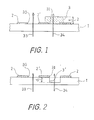
- a typical reticle structure having phase-shifters is shown for example in Fig. 1.
- a light-shielding layer 2 (hereinafter called a shield layer), generally of chromium (Cr) or a chromium compound, is formed by a conventional method.
- a phase-shift layer 3 (hereinafter called a phase-shifter) which has the function of improving the resolution in photolithography.
- Fig. 2 shows a cross-section of another reticle structure with phase-shifters.
- a pattern of light-shielding layers 2 is formed on a glass substrate 1.
- a phase-shifter 3' takes the form of a groove or well formed under a window 31 between two adjacent light-shielding layers 2 and 2'.
- the groove is formed by subjecting the substrate 1 to a conventional anisotropic etching process such as RIE (Reactive Ion Etching), in which only the substrate surface for the groove forming area is exposed and other areas are covered with a resist layer.
- RIE Reactive Ion Etching
- the shield layer includes a missing portion or void portion, or an unnecessary extra portion in its pattern, before forming phase-shifters, these defects are comparatively easily repaired using a focused ion beam (hereinafter, FIB) apparatus.
- FIB focused ion beam
- phase-shifters Once the phase-shifters have been formed, if they include any unnecessary extra portion this can be removed using the above FIB apparatus and the reticle can be repaired. However, if the defect is a missing portion in the phase-shifter pattern, the reticle cannot be repaired easily.
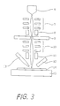
- Ions are emitted from an ion gun 6, gallium (Ga) ions often being used; these are focused by a condenser lens 7 and further on-off controlled by a blanking electrode 8 and a blanking aperture 9.
- An object lens 10 and a deflection lens 11 focus and project an ion beam on to an object 14 to be processed at a specified scanning position.
- the object can be moved by an XY-table 15.
- the ion beam can sputter-and-etch an object material, and a secondary ion detector 12 can detect the object material and is used to identify the ion beam position.
- a gas is introduced from a gas injection gun 13
- the ion beam resolves (decomposes) the gas, and the element thus obtained can be deposited on the object 14.
- phase-shifter 3 of Fig. 1 has a missing portion, or when the groove-shaped phase-shifter 3' of Fig. 2 includes an extra groove portion which should not have been removed, the processes of depositing phase-shifter material or substrate material and repairing the void portion of the phase-shifters are very difficult.
- the thickness of phase-shifter 3 or the depth of phase-shifter 3' is too large (a few hundred nm) to bury the void portion by the FIB apparatus. If it is attempted to deposit silicon dioxide (a popular material for phase-shifters) by the FIB apparatus, the deposited phase-shifter contains gallium; since gallium-containing silicon dioxide is not transparent, it does not work as a phase-shifter.
- EP-A-0 395 425 constitutes prior art for the application under Article 54(3) EPC. It discloses a reticle having a portion formed only by a substrate, a portion formed by the substrate on which is provided a phase-shifter of a first thickness, and a portion formed by the substrate on which is provided a phase shifter of a second thickness.
- US-A-3 547 546 discloses a so-called zone plate used in photolithography for forming patterns such as microcircuits, and having features corresponding to those of the preamble of accompanying claims 1 and 2.
- the zone plate has various zones formed by regions of a transparent plate cut to different thicknesses, providing different phase shifts to transmitted light.
- a reticle suitable for use in projecting a very fine pattern on a semiconductor substrate in photolithography comprising a substrate having a light transparent area which is transparent to projection light used in the photolithography, the light transparent area comprising first, second and third transparent regions through which said projection light is to be transmitted, the first transparent region having a first surface at a first height from a bottom surface of said substrate, the second transparent region having a second surface at a second height from the bottom surface of said substrate corresponding to a top surface of the substrate, wherein said first transparent region gives the projection light transmitted through it a phase difference from the projection light transmitted through said second transparent region, and the third transparent region being selectively patterned and forming a groove in said substrate, and having a third surface at a third height from the bottom surface of said substrate, wherein the third transparent region gives the projection light transmitted through it a phase difference from the projection light transmitted through the second transparent region; characterised in that:
- a reticle suitable for use in projecting a very fine pattern on a semiconductor substrate in photolithography comprising a substrate having a light transparent area which is transparent to projection light used in the photolithography, the light transparent area comprising first, second and third transparent regions through which said projection light is to be transmitted, the first transparent region having a first surface at a first height from a bottom surface of said substrate, the second transparent region being selectively patterned and forming a first groove in said substrate and having a second surface at a second height from the bottom surface of said substrate, wherein said first transparent region gives the projection light transmitted through it a phase difference from the projection light transmitted through said second transparent region, and the third transparent region being selectively patterned and forming a second groove, and having a third surface at a third height from the bottom surface of said substrate, wherein the third transparent region gives the projection light transmitted through it a phase difference from the projection light transmitted through the second transparent region; characterised in that:
- An embodiment of the present invention may thus provide a reticle with phase-shifters which can easily accommodate a small pattern change after completion of reticle fabrication, and which can allow the repair of any pattern defect.
- the present invention also embraces methods of fabricating the above-defined reticles.
- light refers to projection light used in photolithography.
- photolithography in this specification need not be restricted to visible light and can also embrace other forms of radiation and lithography.
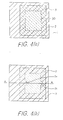
- Figure 4(a) shows a portion of a top view of a reticle with phase-shifters having a correct pattern of a shield layer 2 which has a rectangular outline and a rectangular opening 30.
- the shield layer 2 is formed by depositing Cr layer having a thickness of 60 to 80 nm which is subsequently patterned by a conventional photolithography technique.
- the first embodiment utilizes a positive type phase-shifter 3, therefore, the phase-shifter 3 is formed by depositing a silicon dioxide (SiO 2 ) layer and thereafter the SiO 2 layer is patterned.
- a thickness of the phase-shifter 3 is about 390 nm when i-line rays are used in the stepper. The thickness of the phase-shifter 3 is much larger than that of the shield layer 2.
- Figure 4(b) shows the similar top view of the reticle with phase-shifters as Figure 4(a), however in this case, the shield layer 2 has defective portions 2a and 2b.
- the portion 2a is an extra protrusion and the portion 2b is a missing portion, both being transformed from the normally straight line periphery.
- the shapes of defects in the figure are quite schematic and these defects can be easily repaired if the phase-shifter 3 is not formed on the shield layer 2.
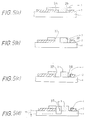
- Figures 5(a) to 5(d) show a cross sectional view at sequential steps of the repair along line A-A in Figure 4(b).
- Figure 5(a) shows a cross section at an initial stage before the repair processes, in which defective portions 2a and 2b in the shield layer 2 are shown by dashed lines.
- the portion of the phase-shifter 3 lying on the extra portion 2a and the portion 2a of the shield layer are removed by a sputter-and-etch method by the previously explained FIB apparatus of Figure 3 forming an opening 37, and thereafter the phase-shifter portion burying the void portion 2b and lying thereon and the neighboring portion on the shield layer 2 are removed using the same apparatus forming an opening 38.
- the exposed surface of the reticle substrate 1 in the opening 37 is subjected to a sputter-and-etch process by the FIB apparatus, resulting in forming a groove having a depth d shown in Figure 5(d).
- the depth d is given as about 3900 angstroms for quartz or glass substrate, which is substantially equal to a thickness t of the positive type deposited SiO 2 phase-shifter.
- thickness t and depth d of the phase-shifters of the present invention are not restricted to the given amount by the equation. Different amounts of thickness or depth for phase-shifters have enough effect of improving the formed pattern on an object.
- Figure 6(a) is a cross sectional view of a reticle with phase-shifters of a positive type, in which a phase-shifter 3 includes a defect of missing portion 3a.
- a thickness t of the phase shifter 3 is given by the above modified calculation using equation (1), and in the actual embodiment of Figure 6(a), since SiO 2 layer is used as the phase-shifter 3, and therefore in this case, the thickness t is about 3900 angstroms.
- the defect portion 3a is repaired by forming a groove having a depth d, which means a negative type phase shifter 3', into the reticle substrate 1 as shown in Figure 6(b).
- the depth d is given by the previous equation (1).
- the negative type phase-shifter 3' can be formed by a sputter-and-etch process utilizing the FIB apparatus.
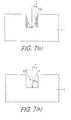
- Figure 7(a) shows an enlarged cross sectional view of the grooved portion 46 only, where the groove shows rather a sharp trench shape having, for example, a width of about 0.2 to 0.4 ⁇ m and a depth of about 0.39 ⁇ m.
- the substrate material such as quartz or glass is sputtered from the substrate and sputtered material again deposits on the sidewall of the groove 46 as shown in Figure 7(a).
- any gas selected among the group of a carbon tetrafluoride gas (CF 4 ), a nitrogen fluoride gas (NF 3 ), a fluorine gas (F 2 ), a sulfur fluoride gas (SF 6 ), a hydrogen fluoride gas (HF), and a chlorine gas (Cl 2 ), is preferably injected from the gas injection gun 13 in the FIB apparatus.
- the object therefor is to remove the substrate material in a volatile silicon compound form such as silicon fluoride (SiF 4 ). This method prevents the substrate material from depositing on the sidewall of the groove.
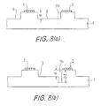
- Figure 8(a) shows a cross sectional view of a reticle with phase-shifters, in which negative type phase-shifters 3 are formed in a reticle substrate 1 between shield layers 2.
- the phase-shifter 3 has a defective portion 3b, which should not be removed in case of forming a correct phase-shifter pattern.
- the depth of the defect portion is increased to 2d, which is twice the normal phase-shifter depth d.
- the depth 2d means that light traveling the distance 2d receives a phase-shift of one full wavelength (2 ⁇ phase-shift), and therefore, it shows the same characteristic as if no phase-shifter is formed at the void portion 3b.
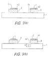
- Figure 9(a) shows a cross sectional view of a reticle with phase-shifters, in which positive type phase-shifters 3 are formed on a reticle substrate 1, and a shield layer 2 of (Cr) is deposited thereon.
- the phase-shifter 3 has a shoulder portion 42 on both sides of the shield layer 2, and one shoulder portion has a defective portion 3c, which should not be taken away when a correct phase-shifter pattern is formed.
- FIG. 10 shows a cross sectional view of a reticle with phase-shifters, in which positive and negative type phase-shifters are formed and no shield layer is used, by way of background explanation.
- a positive type phase-shifter 3 is formed on a reticle substrate 1 and a negative type phase-shifter 3' is formed on both sides of the positive type phase-shifter 3.
- this reticle is not in accordance with the invention, it illustrates that a shield layer is not essential.
Landscapes
- Physics & Mathematics (AREA)
- General Physics & Mathematics (AREA)
- Preparing Plates And Mask In Photomechanical Process (AREA)
- Exposure And Positioning Against Photoresist Photosensitive Materials (AREA)
- Exposure Of Semiconductors, Excluding Electron Or Ion Beam Exposure (AREA)
Claims (14)
- Réticule convenant à une utilisation pour projeter un motif très fin sur un substrat de semiconducteur en photolithographie, le réticule comprenant un substrat (1) comportant une zone transparente à la lumière qui est transparente à la lumière de projection utilisée dans la photolithographie, la zone transparente à la lumière comprenant des première, seconde et troisième régions transparentes au travers desquelles ladite lumière de projection doit être transmise, la première région transparente (3) comportant une première surface à une première hauteur par rapport à une surface inférieure dudit substrat (1), la seconde région transparente comportant une seconde surface à une seconde hauteur par rapport à la surface inférieure dudit substrat correspondant à une surface supérieure du substrat (1), dans lequel ladite première région transparente communique à la lumière de projection transmise au travers de celle-ci une différence de phase par rapport à la lumière de projection transmise au travers de ladite seconde région transparente, et la troisième région transparente étant sélectivement mise en motif en formant une rainure (37, 3', 40) dans ledit substrat, et comportant une troisième surface à une troisième hauteur par rapport à la surface inférieure dudit substrat (1), dans laquelle la troisième région transparente communique à la lumière de projection transmise au travers de celle-ci une différence de phase par rapport à la lumière de projection transmise au travers de la seconde région transparente, caractérisé en ce que :ladite première région transparente (3) est formée en déposant et en mettant en motif sélectivement une couche de déphasage sur ledit substrat (1), etladite troisième région transparente communique à ladite lumière de projection transmise au travers de celle-ci pratiquement la même phase que la lumière de projection transmise au travers de la première région transparente, de façon à réparer une partie défectueuse de ladite première région transparente (3).
- Réticule convenant à une utilisation pour projeter un motif très fin sur un substrat de semiconducteur en photolithographie, le réticule comprenant un substrat (1) comportant une zone transparente à la lumière qui est transparente à la lumière de projection utilisée dans la photolithographie, la zone transparente à la lumière comprenant des première, seconde et troisième régions transparentes au travers desquelles ladite lumière de projection doit être transmise, la première région transparente (3) comportant une première surface à une première hauteur par rapport à une surface inférieure dudit substrat (1), la seconde région transparente étant sélectivement mise en motif et formant une première rainure dans ledit substrat et comportant une seconde surface à une seconde hauteur par rapport à la surface inférieure dudit substrat, dans lequel ladite première région transparente (3) communique à la lumière de projection transmise au travers de celle-ci une différence de phase par rapport à la lumière de projection transmise au travers de ladite seconde région transparente, et la troisième région transparente étant sélectivement mise en motif et formant une seconde rainure (3b), et comportant une troisième surface à une troisième hauteur par rapport à la surface inférieure dudit substrat (1), dans lequel la troisième région transparente communique à la lumière de projection transmise au travers de celle-ci une différence de phase par rapport à la lumière de projection transmise au travers de la seconde région transparente, caractérisé en ce que :la troisième région transparente communique à ladite lumière de projection transmise au travers de celle-ci pratiquement la même phase que la lumière de projection transmise au travers de la première région transparente, de façon à réparer une partie défectueuse de ladite première région transparente (3).
- Réticule selon la revendication 1 ou 2, dans lequel ladite différence de phase entre ladite lumière de projection transmise au travers desdites première et seconde régions transparentes est pratiquement égale à une demi-longueur d'onde de ladite lumière de projection.
- Réticule selon la revendication 1, dans lequel ladite première région transparente et ladite troisième région transparente sont disposées côte à côte de façon à présenter un bord commun.
- Réticule selon l'une quelconque des revendications précédentes, dans lequel ledit substrat (1) est fait de quartz ou de verre.
- Réticule selon la revendication 1, dans lequel ladite couche de déphasage (3) est faite de dioxyde de silicium (SiO2).
- Réticule selon l'une quelconque des revendications précédentes, comprenant en outre une couche de masque de lumière (2) qui est formée sur le substrat (1) et mise en motif afin de définir ladite zone transparente à la lumière.
- Réticule selon la revendication 7, dans lequel ladite couche de masque (2) comprend du chrome.
- Procédé de fabrication du réticule selon la revendication 1, comprenant les étapes consistant à :(a) déposer ladite couche de déphasage (3) sur ledit substrat (1), l'épaisseur de la couche de déphasage étant choisie de façon à produire une différence de phase entre la lumière de projection transmise au travers dudit substrat sans ladite couche de déphasage et la lumière de projection transmise au travers, à la fois dudit substrat et de ladite couche de déphasage,(b) éliminer sélectivement ladite couche de déphasage (3), en définissant ainsi ladite première région transparente dans une zone comportant à la fois ledit substrat (1) et ladite couche de déphasage, et ladite seconde région transparente dans une zone comportant uniquement ledit substrat, et(c) éliminer sélectivement ledit substrat (1) jusqu'à une certaine profondeur de façon à former ladite rainure (37, 3', 40) dans ledit substrat, en définissant ainsi ladite troisième région transparente dans la zone de ladite rainure, dans lequel la lumière de projection transmise au travers de ladite troisième région transparente reçoit pratiquement la même phase que la lumière de projection transmise au travers de ladite première région transparente, ladite troisième région transparente étant formée dans une zone correspondant à la partie défectueuse de ladite première région transparente.
- Procédé de fabrication du réticule selon la revendication 2, comprenant les étapes consistant à :(a) former ladite première rainure (3) dans ledit substrat, en définissant ainsi ladite première région transparente dans la zone du substrat à l'extérieur de ladite première rainure et ladite seconde région transparente dans la zone de ladite première rainure, la profondeur de la première rainure étant choisie de façon à produire une différence de phase entre la lumière de projection transmise au travers de ladite première région transparente et la lumière de projection transmise au travers de ladite seconde région transparente, et(b) former ladite seconde rainure (3b) dans ladite seconde région transparente, en définissant ainsi ladite troisième région transparente dans la zone de ladite seconde rainure, la profondeur de la seconde rainure étant choisie de façon à ce que la lumière de projection transmise au travers de ladite troisième région reçoive la même phase que la lumière de projection transmise au travers de ladite première région transparente, ladite troisième région transparente étant formée dans une zone correspondant à la partie défectueuse de ladite première région transparente.
- Procédé selon la revendication 9, dans lequel ladite étape (c) comprend en outre les sous-étapes consistant à :placer ledit réticule dans un appareil à faisceau d'ions focalisé, l'appareil étant muni d'un pistolet d'injection de gaz,injecter un gaz comprenant un halogène sur ladite partie défectueuse du substrat, etfaire rayonner un faisceau d'ions sur la zone de ladite partie défectueuse afin d'éliminer certains matériaux dans cette zone en formant ainsi ladite troisième région transparente.
- Procédé selon la revendication 11, dans lequel ledit gaz comprenant un halogène est un gaz sélectionné à partir du groupe du gaz de tétrafluorure de carbone (CF4), du gaz de fluorure d'azote (NF3), du gaz de fluor (F2), du gaz de fluorure de soufre (SF6), du gaz de fluorure d'hydrogène (HF), et du gaz de chlore (Cl2).
- Procédé selon la revendication 10, dans lequel ladite étape (b) comprend en outre les sous-étapes consistant à :placer ledit réticule dans un appareil à faisceau d'ions focalisé, l'appareil étant muni d'un pistolet d'injection de gaz,injecter un gaz comprenant un halogène sur ladite partie défectueuse du substrat, etfaire rayonner un faisceau d'ions sur la zone de ladite partie défectueuse afin d'éliminer une partie du substrat dans cette zone, en formant ainsi ladite seconde rainure.
- Procédé selon la revendication 13, dans lequel ledit gaz comprenant un halogène est sélectionné à partir du groupe du gaz de tétrafluorure de carbone (CF4), du gaz de fluorure d'azote (NF3), du gaz de fluor (F2), du gaz de fluorure de soufre (SF6), du gaz de fluorure d'hydrogène (HF), et du gaz de chlore (Cl2).
Applications Claiming Priority (2)
| Application Number | Priority Date | Filing Date | Title |
|---|---|---|---|
| JP16343490 | 1990-06-20 | ||
| JP163434/90 | 1990-06-20 |
Publications (2)
| Publication Number | Publication Date |
|---|---|
| EP0462560A1 EP0462560A1 (fr) | 1991-12-27 |
| EP0462560B1 true EP0462560B1 (fr) | 1998-11-25 |
Family
ID=15773821
Family Applications (1)
| Application Number | Title | Priority Date | Filing Date |
|---|---|---|---|
| EP91109949A Expired - Lifetime EP0462560B1 (fr) | 1990-06-20 | 1991-06-18 | Réticule avec décaleurs de phase et méthode de fabrication |
Country Status (4)
| Country | Link |
|---|---|
| US (2) | US5276551A (fr) |
| EP (1) | EP0462560B1 (fr) |
| KR (1) | KR950000091B1 (fr) |
| DE (1) | DE69130518T2 (fr) |
Families Citing this family (28)
| Publication number | Priority date | Publication date | Assignee | Title |
|---|---|---|---|---|
| DE69131497T2 (de) * | 1990-06-21 | 2000-03-30 | Matsushita Electronics Corp., Kadoma | Photomaske, die in der Photolithographie benutzt wird und ein Herstellungsverfahren derselben |
| US5578402A (en) * | 1990-06-21 | 1996-11-26 | Matsushita Electronics Corporation | Photomask used by photolithography and a process of producing same |
| US5362940A (en) * | 1990-11-09 | 1994-11-08 | Litel Instruments | Use of Fresnel zone plates for material processing |
| US6020950A (en) * | 1992-02-24 | 2000-02-01 | Nikon Corporation | Exposure method and projection exposure apparatus |
| JP3333886B2 (ja) * | 1992-09-17 | 2002-10-15 | ミノルタ株式会社 | ホログラフィ素子 |
| US5403685A (en) * | 1992-09-29 | 1995-04-04 | Sharp Kabushiki Kaisha | Lithographic process for producing small mask apertures and products thereof |
| US5300786A (en) * | 1992-10-28 | 1994-04-05 | International Business Machines Corporation | Optical focus phase shift test pattern, monitoring system and process |
| US5403682A (en) * | 1992-10-30 | 1995-04-04 | International Business Machines Corporation | Alternating rim phase-shifting mask |
| WO1994019723A1 (fr) * | 1993-02-23 | 1994-09-01 | Interuniversitair Micro-Elektronica | Structure de phase optique ameliorant la definition pour un systeme d'eclairage par projection |
| JP3351485B2 (ja) * | 1993-12-10 | 2002-11-25 | 富士通株式会社 | 位相シフトマスクの製造方法 |
| US5532089A (en) * | 1993-12-23 | 1996-07-02 | International Business Machines Corporation | Simplified fabrication methods for rim phase-shift masks |
| KR0128827B1 (ko) * | 1993-12-31 | 1998-04-07 | 김주용 | 위상반전마스크 제조방법 |
| KR970005675B1 (en) * | 1994-01-19 | 1997-04-18 | Hyundai Electronics Ind | Fabrication method of phase shift mask |
| KR0137977B1 (ko) * | 1994-10-12 | 1998-06-15 | 김주용 | 위상반전마스크 및 그 제조방법 |
| JPH08314116A (ja) * | 1995-03-15 | 1996-11-29 | Toshiba Corp | 露光用マスク及びその製造方法 |
| CA2230819C (fr) * | 1995-08-29 | 2009-04-14 | Sumitomo Pharmaceuticals Co., Ltd. | Medicament comprenant le gene hgf |
| JP3290861B2 (ja) * | 1995-09-18 | 2002-06-10 | 株式会社東芝 | 露光用マスクとパターン形成方法 |
| US5935733A (en) * | 1996-04-05 | 1999-08-10 | Intel Corporation | Photolithography mask and method of fabrication |
| US5789117A (en) * | 1996-12-02 | 1998-08-04 | Taiwan Semiconductor Manufacturing Company, Ltd. | Transfer method for non-critical photoresist patterns |
| US6348288B1 (en) * | 2000-04-17 | 2002-02-19 | Taiwan Semiconductor Manufacturing Company | Resolution enhancement method for deep quarter micron technology |
| US6395435B1 (en) | 2000-06-27 | 2002-05-28 | The United States Of America As Represented By The Secretary Of The Navy | Photo-lithographic mask having total internal reflective surfaces |
| KR100374552B1 (ko) * | 2000-08-16 | 2003-03-04 | 주식회사 하이닉스반도체 | 엘리베이티드 소스/드레인을 갖는 반도체 소자 제조방법 |
| JP4149676B2 (ja) * | 2001-02-05 | 2008-09-10 | 株式会社東芝 | フォトマスクの修正方法 |
| US7077973B2 (en) * | 2003-04-18 | 2006-07-18 | Applied Materials, Inc. | Methods for substrate orientation |
| US7147974B2 (en) * | 2003-10-14 | 2006-12-12 | Micron Technology, Inc. | Methods for converting reticle configurations |
| TWI259935B (en) * | 2004-01-08 | 2006-08-11 | Samsung Electronics Co Ltd | Method of adjusting deviation of critical dimension of patterns |
| US7838178B2 (en) | 2007-08-13 | 2010-11-23 | Micron Technology, Inc. | Masks for microlithography and methods of making and using such masks |
| US7970328B2 (en) * | 2007-11-16 | 2011-06-28 | Xerox Corporation | System and method for preparing magnetic ink character recognition readable documents |
Citations (1)
| Publication number | Priority date | Publication date | Assignee | Title |
|---|---|---|---|---|
| US3547546A (en) * | 1966-05-04 | 1970-12-15 | Sprague Electric Co | Multiple image forming device |
Family Cites Families (5)
| Publication number | Priority date | Publication date | Assignee | Title |
|---|---|---|---|---|
| US4530736A (en) * | 1983-11-03 | 1985-07-23 | International Business Machines Corporation | Method for manufacturing Fresnel phase reversal plate lenses |
| JPS60103308A (ja) * | 1983-11-11 | 1985-06-07 | Pioneer Electronic Corp | マイクロフレネルレンズの製造方法 |
| JP2710967B2 (ja) * | 1988-11-22 | 1998-02-10 | 株式会社日立製作所 | 集積回路装置の製造方法 |
| US5234780A (en) * | 1989-02-13 | 1993-08-10 | Kabushiki Kaisha Toshiba | Exposure mask, method of manufacturing the same, and exposure method using the same |
| EP0653679B1 (fr) * | 1989-04-28 | 2002-08-21 | Fujitsu Limited | Masque, méthode de fabrication de masque et méthode pour former des motifs en utilisant le masque |
-
1991
- 1991-06-17 KR KR1019910010007A patent/KR950000091B1/ko not_active Expired - Fee Related
- 1991-06-18 DE DE69130518T patent/DE69130518T2/de not_active Expired - Fee Related
- 1991-06-18 EP EP91109949A patent/EP0462560B1/fr not_active Expired - Lifetime
- 1991-06-18 US US07/716,987 patent/US5276551A/en not_active Expired - Fee Related
-
1993
- 1993-10-19 US US08/138,002 patent/US5514498A/en not_active Expired - Fee Related
Patent Citations (1)
| Publication number | Priority date | Publication date | Assignee | Title |
|---|---|---|---|---|
| US3547546A (en) * | 1966-05-04 | 1970-12-15 | Sprague Electric Co | Multiple image forming device |
Also Published As
| Publication number | Publication date |
|---|---|
| US5514498A (en) | 1996-05-07 |
| EP0462560A1 (fr) | 1991-12-27 |
| DE69130518D1 (de) | 1999-01-07 |
| KR920001633A (ko) | 1992-01-30 |
| KR950000091B1 (ko) | 1995-01-09 |
| DE69130518T2 (de) | 1999-04-22 |
| US5276551A (en) | 1994-01-04 |
Similar Documents
| Publication | Publication Date | Title |
|---|---|---|
| EP0462560B1 (fr) | Réticule avec décaleurs de phase et méthode de fabrication | |
| EP0674223B1 (fr) | Masque à décalage de phase atténuant et procédé de fabrication | |
| US5948574A (en) | Mask for manufacturing semiconductor device and method of manufacture thereof | |
| US6335129B1 (en) | Method for repairing pattern defect, photo mask using the method, and semiconductor device manufacturing method employing the photo mask | |
| US6306547B1 (en) | Photomask and manufacturing method thereof, and exposure method using the photomask | |
| US5382484A (en) | Method of correcting defects in the pattern of phase shift mask | |
| EP0653679A2 (fr) | Masque, méthode de fabrication de masque et méthode pour former des motifs en utilisant le masque | |
| US5405721A (en) | Phase-shifting lithographic masks having phase-shifting layers of differing compositions | |
| US5424153A (en) | Optical mask using phase shift and method of producing the same | |
| EP0922997B1 (fr) | Masque à décalage de phase et procédée fabrication d'un tel masque | |
| US6660437B2 (en) | Alternating phase mask | |
| US7569314B2 (en) | Method for quartz bump defect repair with less substrate damage | |
| US5591549A (en) | Self aligning fabrication method for sub-resolution phase shift mask | |
| US20040086787A1 (en) | Alternating aperture phase shift photomask having plasma etched isotropic quartz features | |
| US20050026053A1 (en) | Photomask having an internal substantially transparent etch stop layer | |
| KR100363090B1 (ko) | 개구부용 포토마스크의 불투명 결함 수리 방법 | |
| US5275895A (en) | Method of manufacturing phase-shifting mask | |
| EP0539006B1 (fr) | Procédé de réparation de masques lithographiques à décalage de phase | |
| JPH0588347A (ja) | レチクル及びその製造方法 | |
| JP3271224B2 (ja) | ハーフトーン型位相シフトマスクの位相シフト量のズレの検出方法 | |
| KR960006818B1 (ko) | 광학 마스크 가공방법 | |
| JPH11258777A (ja) | 光学マスクの欠陥修正方法 | |
| JPH09197651A (ja) | 露光用マスク |
Legal Events
| Date | Code | Title | Description |
|---|---|---|---|
| PUAI | Public reference made under article 153(3) epc to a published international application that has entered the european phase |
Free format text: ORIGINAL CODE: 0009012 |
|
| AK | Designated contracting states |
Kind code of ref document: A1 Designated state(s): DE FR GB IT |
|
| 17P | Request for examination filed |
Effective date: 19911209 |
|
| 17Q | First examination report despatched |
Effective date: 19940617 |
|
| GRAG | Despatch of communication of intention to grant |
Free format text: ORIGINAL CODE: EPIDOS AGRA |
|
| GRAG | Despatch of communication of intention to grant |
Free format text: ORIGINAL CODE: EPIDOS AGRA |
|
| GRAH | Despatch of communication of intention to grant a patent |
Free format text: ORIGINAL CODE: EPIDOS IGRA |
|
| RBV | Designated contracting states (corrected) |
Designated state(s): DE GB |
|
| GRAH | Despatch of communication of intention to grant a patent |
Free format text: ORIGINAL CODE: EPIDOS IGRA |
|
| GRAA | (expected) grant |
Free format text: ORIGINAL CODE: 0009210 |
|
| AK | Designated contracting states |
Kind code of ref document: B1 Designated state(s): DE GB |
|
| REF | Corresponds to: |
Ref document number: 69130518 Country of ref document: DE Date of ref document: 19990107 |
|
| PLBE | No opposition filed within time limit |
Free format text: ORIGINAL CODE: 0009261 |
|
| STAA | Information on the status of an ep patent application or granted ep patent |
Free format text: STATUS: NO OPPOSITION FILED WITHIN TIME LIMIT |
|
| 26N | No opposition filed | ||
| REG | Reference to a national code |
Ref country code: GB Ref legal event code: IF02 |
|
| PGFP | Annual fee paid to national office [announced via postgrant information from national office to epo] |
Ref country code: GB Payment date: 20040616 Year of fee payment: 14 |
|
| PGFP | Annual fee paid to national office [announced via postgrant information from national office to epo] |
Ref country code: DE Payment date: 20040701 Year of fee payment: 14 |
|
| PG25 | Lapsed in a contracting state [announced via postgrant information from national office to epo] |
Ref country code: GB Free format text: LAPSE BECAUSE OF NON-PAYMENT OF DUE FEES Effective date: 20050618 |
|
| PG25 | Lapsed in a contracting state [announced via postgrant information from national office to epo] |
Ref country code: DE Free format text: LAPSE BECAUSE OF NON-PAYMENT OF DUE FEES Effective date: 20060103 |
|
| GBPC | Gb: european patent ceased through non-payment of renewal fee |
Effective date: 20050618 |