EP0464671B1 - Einrichtung zum Nachweis metallischer Unreinheiten auf der Oberfläche eines Halbleitereinkristalls mit Verwendung der Fluoreszenz-Röntgenstrahlentotalreflektion - Google Patents
Einrichtung zum Nachweis metallischer Unreinheiten auf der Oberfläche eines Halbleitereinkristalls mit Verwendung der Fluoreszenz-Röntgenstrahlentotalreflektion Download PDFInfo
- Publication number
- EP0464671B1 EP0464671B1 EP91110658A EP91110658A EP0464671B1 EP 0464671 B1 EP0464671 B1 EP 0464671B1 EP 91110658 A EP91110658 A EP 91110658A EP 91110658 A EP91110658 A EP 91110658A EP 0464671 B1 EP0464671 B1 EP 0464671B1
- Authority
- EP
- European Patent Office
- Prior art keywords
- wafer
- sample
- ray
- stage
- measurement sample
- Prior art date
- Legal status (The legal status is an assumption and is not a legal conclusion. Google has not performed a legal analysis and makes no representation as to the accuracy of the status listed.)
- Expired - Lifetime
Links
- 239000012535 impurity Substances 0.000 title claims description 27
- 239000002184 metal Substances 0.000 title claims description 26
- 229910052751 metal Inorganic materials 0.000 title claims description 26
- 239000013078 crystal Substances 0.000 title claims description 13
- 239000004065 semiconductor Substances 0.000 title claims description 6
- 238000005259 measurement Methods 0.000 claims description 68
- 238000004458 analytical method Methods 0.000 claims description 13
- 230000005284 excitation Effects 0.000 claims description 7
- XUIMIQQOPSSXEZ-UHFFFAOYSA-N Silicon Chemical compound [Si] XUIMIQQOPSSXEZ-UHFFFAOYSA-N 0.000 claims description 6
- 229910052710 silicon Inorganic materials 0.000 claims description 5
- 239000010703 silicon Substances 0.000 claims description 5
- 238000013519 translation Methods 0.000 claims description 3
- 238000000034 method Methods 0.000 description 12
- 238000004876 x-ray fluorescence Methods 0.000 description 10
- 230000035945 sensitivity Effects 0.000 description 9
- 238000013459 approach Methods 0.000 description 5
- 238000001228 spectrum Methods 0.000 description 5
- XEEYBQQBJWHFJM-UHFFFAOYSA-N Iron Chemical compound [Fe] XEEYBQQBJWHFJM-UHFFFAOYSA-N 0.000 description 4
- 230000002035 prolonged effect Effects 0.000 description 4
- KRHYYFGTRYWZRS-UHFFFAOYSA-N Fluorane Chemical compound F KRHYYFGTRYWZRS-UHFFFAOYSA-N 0.000 description 3
- PXHVJJICTQNCMI-UHFFFAOYSA-N Nickel Chemical compound [Ni] PXHVJJICTQNCMI-UHFFFAOYSA-N 0.000 description 3
- 238000010586 diagram Methods 0.000 description 3
- 238000005070 sampling Methods 0.000 description 3
- 238000012360 testing method Methods 0.000 description 3
- GRYLNZFGIOXLOG-UHFFFAOYSA-N Nitric acid Chemical compound O[N+]([O-])=O GRYLNZFGIOXLOG-UHFFFAOYSA-N 0.000 description 2
- 239000002253 acid Substances 0.000 description 2
- 239000012141 concentrate Substances 0.000 description 2
- 239000010949 copper Substances 0.000 description 2
- 239000000463 material Substances 0.000 description 2
- 229910017604 nitric acid Inorganic materials 0.000 description 2
- 230000005855 radiation Effects 0.000 description 2
- NCGICGYLBXGBGN-UHFFFAOYSA-N 3-morpholin-4-yl-1-oxa-3-azonia-2-azanidacyclopent-3-en-5-imine;hydrochloride Chemical compound Cl.[N-]1OC(=N)C=[N+]1N1CCOCC1 NCGICGYLBXGBGN-UHFFFAOYSA-N 0.000 description 1
- RYGMFSIKBFXOCR-UHFFFAOYSA-N Copper Chemical compound [Cu] RYGMFSIKBFXOCR-UHFFFAOYSA-N 0.000 description 1
- WHXSMMKQMYFTQS-UHFFFAOYSA-N Lithium Chemical compound [Li] WHXSMMKQMYFTQS-UHFFFAOYSA-N 0.000 description 1
- 238000002441 X-ray diffraction Methods 0.000 description 1
- 238000010521 absorption reaction Methods 0.000 description 1
- 229910052782 aluminium Inorganic materials 0.000 description 1
- XAGFODPZIPBFFR-UHFFFAOYSA-N aluminium Chemical compound [Al] XAGFODPZIPBFFR-UHFFFAOYSA-N 0.000 description 1
- 229910052790 beryllium Inorganic materials 0.000 description 1
- ATBAMAFKBVZNFJ-UHFFFAOYSA-N beryllium atom Chemical compound [Be] ATBAMAFKBVZNFJ-UHFFFAOYSA-N 0.000 description 1
- 230000000052 comparative effect Effects 0.000 description 1
- 229910052802 copper Inorganic materials 0.000 description 1
- 230000006378 damage Effects 0.000 description 1
- 230000001419 dependent effect Effects 0.000 description 1
- 238000001514 detection method Methods 0.000 description 1
- 238000011161 development Methods 0.000 description 1
- 230000005283 ground state Effects 0.000 description 1
- 229910052744 lithium Inorganic materials 0.000 description 1
- 238000004519 manufacturing process Methods 0.000 description 1
- 238000000691 measurement method Methods 0.000 description 1
- QPJSUIGXIBEQAC-UHFFFAOYSA-N n-(2,4-dichloro-5-propan-2-yloxyphenyl)acetamide Chemical compound CC(C)OC1=CC(NC(C)=O)=C(Cl)C=C1Cl QPJSUIGXIBEQAC-UHFFFAOYSA-N 0.000 description 1
- 229910052759 nickel Inorganic materials 0.000 description 1
- 230000002093 peripheral effect Effects 0.000 description 1
- 238000003908 quality control method Methods 0.000 description 1
- 239000007787 solid Substances 0.000 description 1
- 239000000126 substance Substances 0.000 description 1
- JBQYATWDVHIOAR-UHFFFAOYSA-N tellanylidenegermanium Chemical compound [Te]=[Ge] JBQYATWDVHIOAR-UHFFFAOYSA-N 0.000 description 1
- 230000007704 transition Effects 0.000 description 1
- WFKWXMTUELFFGS-UHFFFAOYSA-N tungsten Chemical compound [W] WFKWXMTUELFFGS-UHFFFAOYSA-N 0.000 description 1
- 229910052721 tungsten Inorganic materials 0.000 description 1
- 239000010937 tungsten Substances 0.000 description 1
Images



Classifications
-
- G—PHYSICS
- G01—MEASURING; TESTING
- G01N—INVESTIGATING OR ANALYSING MATERIALS BY DETERMINING THEIR CHEMICAL OR PHYSICAL PROPERTIES
- G01N23/00—Investigating or analysing materials by the use of wave or particle radiation, e.g. X-rays or neutrons, not covered by groups G01N3/00 – G01N17/00, G01N21/00 or G01N22/00
- G01N23/22—Investigating or analysing materials by the use of wave or particle radiation, e.g. X-rays or neutrons, not covered by groups G01N3/00 – G01N17/00, G01N21/00 or G01N22/00 by measuring secondary emission from the material
- G01N23/223—Investigating or analysing materials by the use of wave or particle radiation, e.g. X-rays or neutrons, not covered by groups G01N3/00 – G01N17/00, G01N21/00 or G01N22/00 by measuring secondary emission from the material by irradiating the sample with X-rays or gamma-rays and by measuring X-ray fluorescence
-
- G—PHYSICS
- G01—MEASURING; TESTING
- G01N—INVESTIGATING OR ANALYSING MATERIALS BY DETERMINING THEIR CHEMICAL OR PHYSICAL PROPERTIES
- G01N2223/00—Investigating materials by wave or particle radiation
- G01N2223/07—Investigating materials by wave or particle radiation secondary emission
- G01N2223/076—X-ray fluorescence
Definitions
- the invention relates to a total reflection fluorescent X-ray analyzing system including an X-ray source, a stage for samples to be analyzed and a detector for allowing X-rays for excitation to be incident onto the surface of a measurement sample comprised of a semiconductor single crystal at an angle less than a total reflection angle to measure a light quantity of fluorescent X-rays from said measurement sample generated by excitation, thus to conduct an analysis with respect to a surface metal impurity of the measurement sample on the basis of the measured result.
- An arrangement for such a system including an X-ray source, a stage for samples to be analyzed and a detector is e.g. disclosed in EP-A-0235640.
- EP-A-0 318 012 discloses an X-ray analyzer conducting both an X-ray fluorescence analysis and X-ray diffraction having an X-ray source, an X-ray guide tube and a sample chamber with a sample table and an X-ray detector disposed therein.
- the sample table is rotatable along an X-direction and a Y-direction for achieving movement of the sample table in these two directions and further rotatable about a Z-direction for inclining the sample surface.
- the X-ray guide tube is constructed such that it collects X-ray emitted from the X-ray source and directs highly parallel X-ray beams to the sample table so that high brilliancy upon analyzing minute parts can be obtained.
- this invention relates to a total reflection of X-ray fluorescence analyzing system, and more particularly to a system for allowing an X-ray to be incident below an angle of total reflection onto, e.g., a silicon (Si) wafer surface to measure a quantity of an excited fluorescent X-rays generated from metal impurity such as chrominum (Cr), iron (Fe), nickel (Ni), copper (Cu), aluminum (Al), or zinc (Zn), etc. on the surface of the wafer to analyze, on the basis of the measured result, the presence and absence of the surface metal impurity, a quantity of the attached surface metal impurity, the kind thereof, or the state of the distribution thereof, etc.
- metal impurity such as chrominum (Cr), iron (Fe), nickel (Ni), copper (Cu), aluminum (Al), or zinc (Zn), etc.
- an analyzing method was conventionally developed to allow X-ray to be incident onto the surface of the wafer to excite metal impurity atoms to measure fluorescent X-ray generated by excitation to carry out an analysis with respect to the surface metal impurity of a measurement sample on the basis of the measured result.
- excitation is used in a sense to give an energy to atoms to conduct a transition thereof from the ground state to a higher energy level.
- the X-ray analyzing method utilize this phenomenon. Since the light quantity of the fluorescent X-ray is proportional to the quantity of an object to be excited, the quantity of the metal impurity attached can be measured by measurement of that light quantity. Further, since the metal impurity has an energy peculiar to the object to be excited, the kind of the metal impurity is made clear by examining that energy.
- an excited X-ray is caused to be partially incident onto the wafer to thereby permit implementation of the positional analysis of the wafer in-place, i.e., the analysis of the state of the in-plane distribution of the metal impurity, or the analysis where the in-plane location of the metal impurity is designated.
- this X-ray analyzing method makes it possible to conduct a more detailed analysis as compared to the above-mentioned chemical analyzing method.
- that wafer can be used as the material of the chip, and implementation of the in-line analyzing system can be realized. For this reason, at present, the approach where the metal impurity analysis on the wafer surface is conducted by the X-ray analyzing method is being the main current.
- the analyzing system for carrying out this analysis is roughly composed of an X-ray source, a spectroscope, and a detector, e.g., Solid State Detector (SSD).
- SSD Solid State Detector
- X-ray from the X-ray source is changed to a monochromatic X-ray, and is incident onto the wafer below an angle of total reflection.
- the SSD is arranged so as to avoid that reflected X-ray, but receive only a fluorescent X-ray excited and generated.
- a light quantity value is provided by a count value of the SSD.
- the wafer subject to analysis is a single crystal, there are instances where the incident X-ray causes the Bragg reflection in dependency upon the incident direction of the X-ray, and the diffracted light thereof is incident to the detector. In this case, since many light quantity values due to the diffracted light which would be the cause of noise are included in measured light quantity value at this detector, there results the problem that the sensitivity is lowered.
- the intensity of an incident light to the detector when the Bragg reflection takes place is 10 to 20 times larger than that when no Bragg reflection takes place.
- the measurement time in the former case is 2 to 10 times larger than that in the latter case.
- the conventional total reflection of X-ray fluorescence analyzing system has the problem that lowered sensitivity or prolonged measurement work is caused by the Bragg reflection.
- this invention has been made, and its object is to provide a total reflection of X-ray fluorescence analyzing system capable of immediately conducting measurement at a high sensitivity.
- a total reflection of X-ray fluorescence analyzing system as mentioned above includes according to this invention measurement sample drive means allowing a combination of a translation movement of the stage in two directions perpendicular to each other, said directions being contained in the plane of the stage supporting the sample, and a rotary movement of the stage in said plane, wherein when it is assumed that an arbitrary interplanar spacing of said measurement sample is d , a wavelength of said X-ray is ⁇ , an irradiation angle that said X-ray and the lattice surface of said measurement sample form is ⁇ , and an arbitrary integer is n , said measurement sample drive means is adapted to carry out positioning of sample points by moving said measurement sample under the state where the orientation with respect to said X-ray of said measurement sample is fixed so as to satisfy the condition described below to thereby allow sample points to be subjected to positioning: 2d sin ⁇ ⁇ n ⁇ .
- the measurement sample drive element is adapted to conduct positioning of sample points by moving the measurement sample thus to determine, under that state, the orientation with respect to the X-ray of the measurement sample so as to satisfy the condition described below: 2d sin ⁇ ⁇ n ⁇ .
- the measurement sample drive element includes a sample stage which can be fixed with respect to incident excited X-rays so as to satisfy the condition described below: 2d sin ⁇ ⁇ n ⁇ .
- the orientation of the measurement sample is set so as to avoid the orientation in which the Bragg reflection takes place. For this reason, there is no possibility that many incident light quantity values by the Bragg reflection which would be noise are included in the measured light quantity value at the detector. Thus, high sensitivity measurement can be conducted.
- reference numeral 1 denotes an X-ray source
- reference numeral 2 a monochromater
- the X-ray source 1 generates continuous X-rays and characteristic X-rays of tungsten (W) as X-rays L 0 .
- W tungsten
- Reference 3 denotes a Si wafer serving as a measurement sample, and reference numeral 4 an XY stage.
- the wafer 3 is horizontally mounted on the upper surface of the XY stage 4, and is fixed by means of the electrostatic chuck.
- the X-rays L 1 from the monochromater 2 are incident onto the wafer 3 wherein the incident angle ⁇ 1 is set to a total reflection angle, i.e., an angle less than a critical angle of silicon. Practically, the incident angle ⁇ 1 is an angle less than 0.2 degrees.
- these X-rays L 1 are reflected on the surface of the wafer 3, resulting in reflected X-rays L 2 , and excite atoms on the surface of the wafer 3 to radiate fluorescent X-rays L 3 .
- a radiation wave from the silicon atoms is generated.
- a radiation wave from the atoms of the metal impurity is generated simultaneously.
- Reference numeral 5 denotes a detector. This detector 5 carries out a count operation by a time corresponding to a light quantity of an incident light. The count value becomes equal to a value corresponding to an energy of an incident light.
- Reference numeral 6 denotes a measurement chamber.
- the wafer 3, the stage 4 and the detector 5 are arranged within the measurement chamber 6.
- the interior of the measurement chamber 6 is kept in a vacuum state of the order of about 10 -2 Torr.
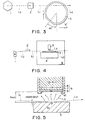
- the detector 5 is composed, as shown in FIG. 5, of a detecting element 7 comprised of a semiconductor of silicon (Si) including lithium (Li) etc., a casing 8 for accommodating the element 7, and an opening portion 10 bored in the bottom portion of the casing 8. This opening portion 10 is opened facing the wafer 3. Between the opening portion 10 and the element 7, a beryllium (Be) plate 9 is inserted. A window is constituted by the Be plate 9 and the opening portion 10. Fluorescent X-rays L 3 from the wafer 3 are incident to the element 7 through the window.
- a detecting element 7 comprised of a semiconductor of silicon (Si) including lithium (Li) etc.
- a casing 8 for accommodating the element 7, and an opening portion 10 bored in the bottom portion of the casing 8. This opening portion 10 is opened facing the wafer 3.
- Be beryllium
- a gap for permitting X-rays L 1 and L 2 to be passed therethrough is provided between the lower end of the opening portion 10 and the upper surface of the wafer 3.
- This gap is set as small as possible in order to increase the detection sensitivity. In this embodiment, the gap is 5 mm.
- the diameter of the opening portion 10 is set to 1 cm in the embodiment. Light in the range from a vertical direction to a direction inclined by 45 degrees thereto when viewed from the measurement position (i.e., the incident position of the X-ray L 1 ) indicated by reference symbol P in FIG. 5 is permitted to be passed through the opening portion 10.
- the element 7 outputs a signal of the voltage level corresponding to an incident light quantity to deliver it to a voltage controlled counter (not shown) which carries out a count operation by a time corresponding to the input voltage level.
- FIG. 1 is an explanatory view showing the essential part of a system according to a first embodiment of this invention.
- the Si wafer 3 is rotated as indicated by arrows r 1 and r 0 by the rotation of the XY stage 4.
- the orientation with respect to the X-rays L 1 is set.
- the Si wafer 3 is moved in a two-dimensional manner by horizontal movement in the X- and Y- directions of the XY stage 4.
- respective sample points of the Si wafer 3 are subjected to positioning so that they are located at the measurement position P.
- the orientation with respect to the X-ray L 1 of the wafer 3 is set so as to satisfy the following condition: 2d sin ⁇ ⁇ n ⁇
- the positions rotated in succession by 90 degrees from the determined angle are considered as the position where the Bragg reflection is strong.
- Si wafer having, e.g., the lattice plane (100) four positions of the position of zero degrees which is the center position of the orientation flat, and positions rotated in succession by 90 degrees from the angle, i.e., positions of 90, 180 and 270 degrees are considered as the position where the Bragg reflection is strong.
- the sample points of the wafer 3 are adapted to be subjected to positioning by horizontally moving the XY stage in X- and Y- directions under the state where the orientation with respect to the X-ray L 1 is fixed.
- the distribution measurement of the metal impurity is conducted in connection with 21 sample points on the surface of the wafer 3 wherein the measurement time is set to one hour and half (about 250 seconds per each point) as a set value.
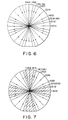
- FIG. 6 shows the orientations, each indicated by an arrow and shows the lattice planes which cause diffraction, each indicated by (hK1), in which an intensive diffracted light is caused to be incident to the detector wherein these orientations are obtained as the result of the fact that X-rays L 1 are caused to be incident to the wafer 3 in various orientations.
- the wafer 3 is attached at first on the stage 4 at the orientation where the center of the orientation flat of the wafer is on the directional line do thereafter to rotate the stage 4 by about 40 degrees in a r 0 direction to set the orientation of the wafer 3.
- the stage 4 is moved in X- and Y-directions to allow respective sample points of in-plane 21 points of the wafer 3 to be subjected to positioning so that they are located at the measurement position P, thus to carry out measurement.
- FIG. 8 shows count values per unit time at respective sample points by the conventional system
- FIG. 9 shows count values per unit time at respective sample points by the system of the first embodiment. It is seen from these figures that, in the case of the conventional system, the count value is extremely high at the sampling point corresponding to the regions where the above-mentioned diffraction takes place, whereas, in the case of the system of the first embodiment, mean values appear at the respective sample points.
- FIG. 10 is a curve showing a spectrum with respect to the sample points to which the symbol ⁇ is attached in FIG. 8
- FIG. 11 is a curve diagram obtained by enlarging the scale of FIG. 10
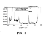
- FIG. 12 is a curve the spectrum with respect to sample points to which the symbol ⁇ is attached in FIG. 9.
- the maximum count value is equal to 248.4000 cps. This value is extremely high as compared to 42.1900 cps of FIG. 12. The measurement time is prolonged accordingly.
- the peak of Fe was discriminated, and it was confirmed by measurement that the concentration of Fe is 3 x 10 10 to 5 x 10 10 [atoms/cm 2 ].
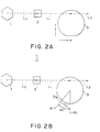
- FIG. 2 is an explanatory view showing the essential part of a system according to a second embodiment of this invention.
- the wafer 3 is first rotated in a r 0 -r 1 direction where the orientation with respect to the incident X-ray L 0 is fixed, and then move in X- and Y- directions to position the wafer 3.
- the wafer 3 is first moved in an X- Y- directions to allow the sample points to be subjected to positioning to rotate the wafer 3 in a r 0 -r 1 direction under that state so as to satisfy the condition of 2d sin ⁇ ⁇ n ⁇ to determine the orientation with respect to the incident X-ray L 0 as shown in FIG. 2B.
- the stage 4 is first moved in X- and Y- directions to allow respective sampling points of in-plane 21 points of the wafer 3 to be subjected to positioning so that they are located at the measurement point P to attach, under this state, the wafer 3 on the state 4 as a temporary measure at the orientation where the center of the orientation flat is positioned on the directional line d 0 thereafter to rotate the stage 4 by about 40 degrees in a r 0 direction to set the orientation of the wafer 3, thus to conduct a measurement.
- Fig. 3 is an explanatory view showing the essential part of a total reflection of X-ray fluorescence analyzing system not an embodiment of the claimed invention. Namely, it is additionally described with reference to Fig. 3 that the stage for positioning of sample points and the stage for determination of orientation may be conducted in an arbitrary order, i.e., irrespective of whether or not either of these stages is conducted precedingly or succeedingly.
- the total reflection X-ray analyzing system shown in FIG. 3 is characterized in that the system includes a sample stage 4' fixed with respect to an incident excited X-ray so as to satisfy the condition of 2d sin ⁇ ⁇ n ⁇ .
- This stage 4' includes a linear side edge corresponding to the orientation flat of the wafer 3.
- the stage 4' is driven in X- and Y- directions to allow the sample points to be subjected to positioning. It is to be noted that the stage 4' of the system is not necessarily required to be driven in the r 0 -r 1 direction. There may be employed an arrangement such that the stage 4' is driven only for adjustment. In addition, an arrangement such that adjustment can be manually made is basically sufficient for this purpose.
- the orientation of the measurement sample is set so as to avoid the orientations where the Bragg reflection takes place. Accordingly, the possibility that many incident light quantity values due to the Bragg reflection which would be the cause of noise are included in the measured light quantity values at the detector is eliminated. Thus, high sensitivity measurement can be conducted.
Landscapes
- Physics & Mathematics (AREA)
- Health & Medical Sciences (AREA)
- Life Sciences & Earth Sciences (AREA)
- Chemical & Material Sciences (AREA)
- Analytical Chemistry (AREA)
- Biochemistry (AREA)
- General Health & Medical Sciences (AREA)
- General Physics & Mathematics (AREA)
- Immunology (AREA)
- Pathology (AREA)
- Analysing Materials By The Use Of Radiation (AREA)
Claims (6)
- Totalreflexionsfluoreszenz-Röntgenanalysesystem mit einer Röntgenstrahlenquelle (1), einem Objekttisch (4) für zu analysierende Proben und einem Detektor (5), um Röntgenstrahlen (L1) zur Anregung auf die Oberfläche einer Meßprobe (3) bestehend aus einem Halbleiter-Einkristall in einem Winkel kleiner als ein Totalreflexionswinkel zum Messen einer Lichtmenge von Fluoreszenz-Röntgenstrahlen (L3) von der Meßprobe, erzeugt durch Anregung, um auf diese Weise eine Analyse bezüglich einer Metallverunreinigung der Oberfläche der Meßprobe (3) auf der Basis des gemessenen Ergebnisses auszuführen,
dadurch gekennzeichnet, daß es aufweist:
eine Meßprobenantriebseinrichtung, welche eine Kombination einer Translationsbewegung des Objekttisches in zwei Richtungen rechtwinklig zueinander, wobei diese Richtungen in der Ebene des die Probe unterstützenden Objekttisches enthalten sind, und einer Rotationsbewegung des Objekttisches in dieser Ebene ermöglicht, wobei dann, wenn angenommen wird, daß ein beliebiger Zwischenebenenabstand der Meßprobe gleich d ist, eine Wellenlänge der Röntgenstrahlen gleich λ ist, ein Bestrahlungswinkel, den die Röntgenstrahlen (L1) und die Gitteroberfläche der Meßprobe bilden, gleich θ ist, und eine beliebige ganze Zahl gleich n ist, die Meßprobenantriebseinrichtung (4) so ausgelegt ist, daß sie eine Positionierung von Probenpunkten durch Bewegen der Meßprobe (3) in dem Zustand ausführt, bei dem die Orientierung der Meßprobe bezogen auf die Röntgenstrahlen (L1) fixiert ist, so daß die nachstehend beschriebene Bedingung erfüllt wird, und durch ermöglicht, daß Probenpunkte (P) einer Positionierung unterworfen werden:
- System nach Anspruch 1, wobei der als Meßprobe dienende Halbleiter-Einkristall als ein vollständiger Einkristall in der Form einer dünnen Scheibe ausgebildet ist und aus einem Silizium-(Si)-Wafer mit einer (100)-Kristallorientierung besteht.
- System nach Anspruch 2,wobei die Meßprobenantriebseinrichtung (4) aus einem Rotationsmechanismus besteht, auf welchem der Wafer befestigt ist, der Rotationsmechanismus angepaßt ist, den Wafer in der Ebene des die Meßprobe tragenden Objekttisches zu drehen, um die Orientierung so zu fixieren, daß sie der genannten Bedingung entspricht, undwobei die Positionierungseinrichtung aus einem Tisch für eine Translationsbewegung in der Ebene des die Probe haltenden Objekttisches besteht, in welchem die Rotationseinrichtung eingebaut ist, und die Positionierungseinrichtung angepaßt ist, den Wafer in den zwei Richtungen rechtwinklig zueinander in dem Zustand zu transportieren, bei dem die Orientierung fixiert ist, um zu ermöglichen, daß mehrere Probenpunkte des Wafers einer Positionierung unterworfen werden.
- System nach Anspruch 3, wobei die Orientierung des Wafers fixiert durch die Drehung des Wafers mittels des Rotationsmechanismus, vier Orientierungen von 0, 90, 180 und 270 Grad eines (100)-Si-Wafers umfaßt.
- System nach Anspruch 2,wobei die Positionierungseinrichtung aus einem Objekttisch zum Bewegen des darauf befestigten Wafers in den zwei Richtungen rechtwinklig zueinander besteht, um zu ermöglichen, daß mehrere Probenpunkte des Wafers einer Positionierung unterworfen werden, undwobei die Meßprobenantriebseinrichtung (4) aus einem Rotationsmechanismus besteht, der an dem Objekttisch zum Drehen des Objekttisches in der Ebene des den Wafer tragenden Objekttisches angebracht ist, um die Orientierung des Wafers so zu fixieren, daß die genannte Bedingung erfüllt wird.
- System nach Anspruch 2,
wobei die Positionierungseinrichtung und die Meßprobenantriebseinrichtung (4) aus einem Probenobjekttisch besteht, der eine Seitenkante enthält, die der Orientierungsabflachung des Wafers als dem Einkristall-Halbleiter entspricht, und es ermöglicht, daß der Wafer einer Positionierung und Fixierung unterworfen wird, so daß ein Einfallswinkel von Röntgenstrahlen zur Anregung, die auf den Wafer einfallen, der so montiert ist, daß die Richtung der Seitenkante und die der Orientierungsabflachung miteinander übereinstimmen, die Bedingung
Applications Claiming Priority (4)
| Application Number | Priority Date | Filing Date | Title |
|---|---|---|---|
| JP170687/90 | 1990-06-28 | ||
| JP17068790 | 1990-06-28 | ||
| JP85469/91 | 1991-04-17 | ||
| JP3085469A JP2535675B2 (ja) | 1990-06-28 | 1991-04-17 | 全反射蛍光x線分析装置 |
Publications (3)
| Publication Number | Publication Date |
|---|---|
| EP0464671A2 EP0464671A2 (de) | 1992-01-08 |
| EP0464671A3 EP0464671A3 (en) | 1992-09-16 |
| EP0464671B1 true EP0464671B1 (de) | 1997-12-29 |
Family
ID=26426475
Family Applications (1)
| Application Number | Title | Priority Date | Filing Date |
|---|---|---|---|
| EP91110658A Expired - Lifetime EP0464671B1 (de) | 1990-06-28 | 1991-06-27 | Einrichtung zum Nachweis metallischer Unreinheiten auf der Oberfläche eines Halbleitereinkristalls mit Verwendung der Fluoreszenz-Röntgenstrahlentotalreflektion |
Country Status (4)
| Country | Link |
|---|---|
| US (1) | US5148457A (de) |
| EP (1) | EP0464671B1 (de) |
| JP (1) | JP2535675B2 (de) |
| DE (1) | DE69128501T2 (de) |
Families Citing this family (13)
| Publication number | Priority date | Publication date | Assignee | Title |
|---|---|---|---|---|
| JP2613513B2 (ja) | 1991-11-05 | 1997-05-28 | 理学電機工業株式会社 | 蛍光x線の分析方法 |
| JPH07153692A (ja) * | 1993-11-30 | 1995-06-16 | Toshiba Corp | 半導体基板上に薄膜を成長させる方法および装置 |
| JP3249316B2 (ja) * | 1993-12-20 | 2002-01-21 | 株式会社東芝 | 全反射蛍光x線分析が行われる被測定体の表面処理方法 |
| JP3051013B2 (ja) * | 1993-12-21 | 2000-06-12 | 株式会社東芝 | 不純物分析方法 |
| JP2843529B2 (ja) * | 1994-07-06 | 1999-01-06 | 理学電機工業株式会社 | 蛍光x線分析装置 |
| US6040198A (en) * | 1995-11-30 | 2000-03-21 | Fujitsu Limited | Element concentration measuring method and apparatus, and semiconductor device fabrication method and apparatus |
| US6055293A (en) * | 1998-06-30 | 2000-04-25 | Seh America, Inc. | Method for identifying desired features in a crystal |
| US6760403B2 (en) | 2001-10-25 | 2004-07-06 | Seh America, Inc. | Method and apparatus for orienting a crystalline body during radiation diffractometry |
| US7027557B2 (en) * | 2004-05-13 | 2006-04-11 | Jorge Llacer | Method for assisted beam selection in radiation therapy planning |
| KR101061425B1 (ko) * | 2006-07-12 | 2011-09-01 | 포항공과대학교 산학협력단 | X-선을 이용한 명시야 촬영 방법 |
| JP4884553B1 (ja) * | 2010-08-31 | 2012-02-29 | 株式会社リガク | X線分析装置および方法 |
| JP5092052B1 (ja) | 2011-11-14 | 2012-12-05 | 株式会社リガク | X線分析装置および方法 |
| CN111670359B (zh) * | 2018-01-31 | 2023-10-10 | 富士胶片株式会社 | 分析方法、药液及药液的制造方法 |
Citations (2)
| Publication number | Priority date | Publication date | Assignee | Title |
|---|---|---|---|---|
| EP0423803A2 (de) * | 1989-10-19 | 1991-04-24 | Sumitomo Electric Industries, Ltd. | Röntgenstrahlen-Fluoreszenzgerät unter Verwendung der Totalreflexion |
| EP0456897A1 (de) * | 1990-05-15 | 1991-11-21 | Siemens Aktiengesellschaft | Messanordnung für die Röntgenfluoreszenzanalyse |
Family Cites Families (5)
| Publication number | Priority date | Publication date | Assignee | Title |
|---|---|---|---|---|
| DE2632001C3 (de) * | 1976-07-16 | 1980-10-23 | Gkss - Forschungszentrum Geesthacht Gmbh, 2000 Hamburg | Meßanordnung zur Röntgenfluoreszenzanalyse |
| DE2727505A1 (de) * | 1977-06-18 | 1979-01-04 | Ibm Deutschland | Roentgenfluoreszenzanalyse zur untersuchung oberflaechennaher schichten |
| DE3606748C1 (de) * | 1986-03-01 | 1987-10-01 | Geesthacht Gkss Forschung | Anordnung zur zerstoerungsfreien Messung von Metallspuren |
| JP2592931B2 (ja) * | 1988-09-30 | 1997-03-19 | キヤノン株式会社 | 蛍光x線分析装置 |
| EP0372278A3 (de) * | 1988-12-02 | 1991-08-21 | Gkss-Forschungszentrum Geesthacht Gmbh | Verfahren und Anordung zur Untersuchung von Proben nach der Methode der Röntgenfluoreszenzanalyse |
-
1991
- 1991-04-17 JP JP3085469A patent/JP2535675B2/ja not_active Expired - Lifetime
- 1991-06-27 DE DE69128501T patent/DE69128501T2/de not_active Expired - Lifetime
- 1991-06-27 US US07/719,706 patent/US5148457A/en not_active Expired - Lifetime
- 1991-06-27 EP EP91110658A patent/EP0464671B1/de not_active Expired - Lifetime
Patent Citations (2)
| Publication number | Priority date | Publication date | Assignee | Title |
|---|---|---|---|---|
| EP0423803A2 (de) * | 1989-10-19 | 1991-04-24 | Sumitomo Electric Industries, Ltd. | Röntgenstrahlen-Fluoreszenzgerät unter Verwendung der Totalreflexion |
| EP0456897A1 (de) * | 1990-05-15 | 1991-11-21 | Siemens Aktiengesellschaft | Messanordnung für die Röntgenfluoreszenzanalyse |
Also Published As
| Publication number | Publication date |
|---|---|
| US5148457A (en) | 1992-09-15 |
| JP2535675B2 (ja) | 1996-09-18 |
| JPH0566204A (ja) | 1993-03-19 |
| EP0464671A2 (de) | 1992-01-08 |
| DE69128501T2 (de) | 1998-05-14 |
| DE69128501D1 (de) | 1998-02-05 |
| EP0464671A3 (en) | 1992-09-16 |
Similar Documents
| Publication | Publication Date | Title |
|---|---|---|
| Iida et al. | Synchrotron X-ray muprobe and its application to human hair analysis | |
| EP0423803B1 (de) | Röntgenstrahlen-Fluoreszenzgerät unter Verwendung der Totalreflexion | |
| US5148457A (en) | System for analyzing metal impurity on the surface of a single crystal semiconductor by using total reflection of x-rays fluorescence | |
| Cohen et al. | Tunable laboratory extended x‐ray absorption fine structure system | |
| DE19948382A1 (de) | Detektor für grosse Waferflächen | |
| De Pauw et al. | A review of laboratory, commercially available, and facility based wavelength dispersive X-ray fluorescence spectrometers | |
| US6628748B2 (en) | Device and method for analyzing atomic and/or molecular elements by means of wavelength dispersive X-ray spectrometric devices | |
| Haschke et al. | Description of a new Micro-XRay spectrometer | |
| Streli et al. | First results of TXRF measurements of low‐Z elements on Si wafer surfaces at the PTB plane grating monochromator beamline for undulator radiation at BESSY II | |
| EP0697109B1 (de) | Röntgenspektrometer mit streifendem ausfallwinkel | |
| KR950010390B1 (ko) | 전반사 형광 x선 분석 장치 | |
| JP3127875B2 (ja) | 全反射螢光x線分析方法及び装置 | |
| GB2343825A (en) | X-ray micro-diffraction apparatus comprising a cylindrical surrounding the specimen | |
| Kujala et al. | High resolution short focal distance Bent Crystal Laue Analyzer for copper K edge x-ray absorption spectroscopy | |
| JPH0792112A (ja) | X線評価装置 | |
| Barstad et al. | Sensitive, Quantitative Recording X‐Ray Spectrometer | |
| JP5846469B2 (ja) | 全反射蛍光x線分析装置及び全反射蛍光x線分析方法 | |
| Laderman et al. | High-sensitivity total reflection X-ray fluorescence spectroscopy of silicon wafers using synchrotron radiation | |
| JPH06160312A (ja) | X線評価装置 | |
| Birks et al. | Development of X-ray fluorescence spectroscopy for elemental analysis of particulate matter in the atmosphere and in source emissions | |
| Taniguchi | Soft x-ray grating spectrometer for secondary-excitation using synchrotron radiation | |
| JP3195046B2 (ja) | 全反射状態の検出方法および微量元素の測定装置 | |
| JPH0434349A (ja) | 蛍光x線分析装置 | |
| JPH0980000A (ja) | X線評価装置 | |
| Hyde et al. | A NEW X-RAY SPECTROGRAPHIC TECHNIQUE APPLIED TO THE ELEMENTARY ANALYSIS OP MILLIGRAM SCALE SAMPLES |
Legal Events
| Date | Code | Title | Description |
|---|---|---|---|
| PUAI | Public reference made under article 153(3) epc to a published international application that has entered the european phase |
Free format text: ORIGINAL CODE: 0009012 |
|
| 17P | Request for examination filed |
Effective date: 19910627 |
|
| AK | Designated contracting states |
Kind code of ref document: A2 Designated state(s): DE FR GB |
|
| RIN1 | Information on inventor provided before grant (corrected) |
Inventor name: KAGEYAMA, MOKUJI Inventor name: SAMATA, SHUICHI Inventor name: MATSUSHITA, YOSHIAKI Inventor name: TSUCHIYA, NORIHIKO Inventor name: KUBOTA, ATSUKO |
|
| PUAL | Search report despatched |
Free format text: ORIGINAL CODE: 0009013 |
|
| AK | Designated contracting states |
Kind code of ref document: A3 Designated state(s): DE FR GB |
|
| 17Q | First examination report despatched |
Effective date: 19941114 |
|
| GRAG | Despatch of communication of intention to grant |
Free format text: ORIGINAL CODE: EPIDOS AGRA |
|
| GRAG | Despatch of communication of intention to grant |
Free format text: ORIGINAL CODE: EPIDOS AGRA |
|
| GRAH | Despatch of communication of intention to grant a patent |
Free format text: ORIGINAL CODE: EPIDOS IGRA |
|
| GRAH | Despatch of communication of intention to grant a patent |
Free format text: ORIGINAL CODE: EPIDOS IGRA |
|
| GRAA | (expected) grant |
Free format text: ORIGINAL CODE: 0009210 |
|
| AK | Designated contracting states |
Kind code of ref document: B1 Designated state(s): DE FR GB |
|
| REF | Corresponds to: |
Ref document number: 69128501 Country of ref document: DE Date of ref document: 19980205 |
|
| ET | Fr: translation filed | ||
| PLBQ | Unpublished change to opponent data |
Free format text: ORIGINAL CODE: EPIDOS OPPO |
|
| PLBI | Opposition filed |
Free format text: ORIGINAL CODE: 0009260 |
|
| PLBF | Reply of patent proprietor to notice(s) of opposition |
Free format text: ORIGINAL CODE: EPIDOS OBSO |
|
| REG | Reference to a national code |
Ref country code: GB Ref legal event code: 746 Effective date: 19981010 |
|
| 26 | Opposition filed |
Opponent name: GKSS-FORSCHUNGSZENTRUM GEESTHACHT GMBH Effective date: 19980928 |
|
| PLBF | Reply of patent proprietor to notice(s) of opposition |
Free format text: ORIGINAL CODE: EPIDOS OBSO |
|
| REG | Reference to a national code |
Ref country code: FR Ref legal event code: D6 |
|
| PLBO | Opposition rejected |
Free format text: ORIGINAL CODE: EPIDOS REJO |
|
| APAC | Appeal dossier modified |
Free format text: ORIGINAL CODE: EPIDOS NOAPO |
|
| APAE | Appeal reference modified |
Free format text: ORIGINAL CODE: EPIDOS REFNO |
|
| APAC | Appeal dossier modified |
Free format text: ORIGINAL CODE: EPIDOS NOAPO |
|
| REG | Reference to a national code |
Ref country code: GB Ref legal event code: IF02 |
|
| APBU | Appeal procedure closed |
Free format text: ORIGINAL CODE: EPIDOSNNOA9O |
|
| PLBN | Opposition rejected |
Free format text: ORIGINAL CODE: 0009273 |
|
| STAA | Information on the status of an ep patent application or granted ep patent |
Free format text: STATUS: OPPOSITION REJECTED |
|
| 27O | Opposition rejected |
Effective date: 20030625 |
|
| APAH | Appeal reference modified |
Free format text: ORIGINAL CODE: EPIDOSCREFNO |
|
| PGFP | Annual fee paid to national office [announced via postgrant information from national office to epo] |
Ref country code: FR Payment date: 20100709 Year of fee payment: 20 |
|
| PGFP | Annual fee paid to national office [announced via postgrant information from national office to epo] |
Ref country code: GB Payment date: 20100623 Year of fee payment: 20 Ref country code: DE Payment date: 20100625 Year of fee payment: 20 |
|
| REG | Reference to a national code |
Ref country code: DE Ref legal event code: R071 Ref document number: 69128501 Country of ref document: DE |
|
| REG | Reference to a national code |
Ref country code: DE Ref legal event code: R071 Ref document number: 69128501 Country of ref document: DE |
|
| REG | Reference to a national code |
Ref country code: GB Ref legal event code: PE20 Expiry date: 20110626 |
|
| PG25 | Lapsed in a contracting state [announced via postgrant information from national office to epo] |
Ref country code: GB Free format text: LAPSE BECAUSE OF EXPIRATION OF PROTECTION Effective date: 20110626 |
|
| PG25 | Lapsed in a contracting state [announced via postgrant information from national office to epo] |
Ref country code: DE Free format text: LAPSE BECAUSE OF EXPIRATION OF PROTECTION Effective date: 20110628 |