EP0465290B1 - Verfahren zum Herstellen eines Leistungskondensators - Google Patents
Verfahren zum Herstellen eines Leistungskondensators Download PDFInfo
- Publication number
- EP0465290B1 EP0465290B1 EP91401635A EP91401635A EP0465290B1 EP 0465290 B1 EP0465290 B1 EP 0465290B1 EP 91401635 A EP91401635 A EP 91401635A EP 91401635 A EP91401635 A EP 91401635A EP 0465290 B1 EP0465290 B1 EP 0465290B1
- Authority
- EP
- European Patent Office
- Prior art keywords
- process according
- film
- metallized
- winding
- impregnation
- Prior art date
- Legal status (The legal status is an assumption and is not a legal conclusion. Google has not performed a legal analysis and makes no representation as to the accuracy of the status listed.)
- Expired - Lifetime
Links
- 239000003990 capacitor Substances 0.000 title claims abstract description 26
- 238000000034 method Methods 0.000 title claims description 18
- 238000004519 manufacturing process Methods 0.000 title claims description 11
- 239000007788 liquid Substances 0.000 claims abstract description 9
- 229920006255 plastic film Polymers 0.000 claims abstract description 7
- 239000002985 plastic film Substances 0.000 claims abstract description 7
- 239000010408 film Substances 0.000 claims description 18
- 238000005470 impregnation Methods 0.000 claims description 14
- 238000004804 winding Methods 0.000 claims description 14
- 239000011104 metalized film Substances 0.000 claims description 9
- 229910052751 metal Inorganic materials 0.000 claims description 6
- 239000002184 metal Substances 0.000 claims description 6
- 239000004743 Polypropylene Substances 0.000 claims description 4
- 239000011810 insulating material Substances 0.000 claims description 4
- -1 polypropylene Polymers 0.000 claims description 4
- 229920001155 polypropylene Polymers 0.000 claims description 4
- 235000019484 Rapeseed oil Nutrition 0.000 claims description 3
- QSHDDOUJBYECFT-UHFFFAOYSA-N mercury Chemical compound [Hg] QSHDDOUJBYECFT-UHFFFAOYSA-N 0.000 claims description 3
- 229910052753 mercury Inorganic materials 0.000 claims description 3
- 238000007654 immersion Methods 0.000 claims description 2
- 229920006254 polymer film Polymers 0.000 claims description 2
- 238000001035 drying Methods 0.000 claims 2
- 238000009924 canning Methods 0.000 claims 1
- 230000001747 exhibiting effect Effects 0.000 claims 1
- 238000005507 spraying Methods 0.000 claims 1
- 238000001291 vacuum drying Methods 0.000 claims 1
- 235000008429 bread Nutrition 0.000 description 12
- 238000001465 metallisation Methods 0.000 description 4
- 230000008929 regeneration Effects 0.000 description 4
- 238000011069 regeneration method Methods 0.000 description 4
- 239000004593 Epoxy Substances 0.000 description 3
- IJGRMHOSHXDMSA-UHFFFAOYSA-N Atomic nitrogen Chemical compound N#N IJGRMHOSHXDMSA-UHFFFAOYSA-N 0.000 description 2
- RYGMFSIKBFXOCR-UHFFFAOYSA-N Copper Chemical compound [Cu] RYGMFSIKBFXOCR-UHFFFAOYSA-N 0.000 description 2
- HCHKCACWOHOZIP-UHFFFAOYSA-N Zinc Chemical compound [Zn] HCHKCACWOHOZIP-UHFFFAOYSA-N 0.000 description 2
- 239000002671 adjuvant Substances 0.000 description 2
- 229910052782 aluminium Inorganic materials 0.000 description 2
- XAGFODPZIPBFFR-UHFFFAOYSA-N aluminium Chemical compound [Al] XAGFODPZIPBFFR-UHFFFAOYSA-N 0.000 description 2
- 238000004140 cleaning Methods 0.000 description 2
- 239000011701 zinc Substances 0.000 description 2
- 229910000831 Steel Inorganic materials 0.000 description 1
- PNEYBMLMFCGWSK-UHFFFAOYSA-N aluminium oxide Inorganic materials [O-2].[O-2].[O-2].[Al+3].[Al+3] PNEYBMLMFCGWSK-UHFFFAOYSA-N 0.000 description 1
- 239000003963 antioxidant agent Substances 0.000 description 1
- 230000003078 antioxidant effect Effects 0.000 description 1
- 125000003118 aryl group Chemical group 0.000 description 1
- 230000015572 biosynthetic process Effects 0.000 description 1
- 239000002775 capsule Substances 0.000 description 1
- 238000010411 cooking Methods 0.000 description 1
- 229910052802 copper Inorganic materials 0.000 description 1
- 239000010949 copper Substances 0.000 description 1
- 239000011889 copper foil Substances 0.000 description 1
- 238000009826 distribution Methods 0.000 description 1
- 239000004744 fabric Substances 0.000 description 1
- 239000011521 glass Substances 0.000 description 1
- 239000000463 material Substances 0.000 description 1
- 239000000203 mixture Substances 0.000 description 1
- 229910052757 nitrogen Inorganic materials 0.000 description 1
- 239000005026 oriented polypropylene Substances 0.000 description 1
- 239000004033 plastic Substances 0.000 description 1
- 238000002360 preparation method Methods 0.000 description 1
- 238000005096 rolling process Methods 0.000 description 1
- 238000005476 soldering Methods 0.000 description 1
- 229910001220 stainless steel Inorganic materials 0.000 description 1
- 239000010935 stainless steel Substances 0.000 description 1
- 238000010025 steaming Methods 0.000 description 1
- 239000010959 steel Substances 0.000 description 1
- 238000003786 synthesis reaction Methods 0.000 description 1
- 238000011282 treatment Methods 0.000 description 1
- 235000013311 vegetables Nutrition 0.000 description 1
- 238000003466 welding Methods 0.000 description 1
- 229910052725 zinc Inorganic materials 0.000 description 1
Images

Classifications
-
- H—ELECTRICITY
- H01—ELECTRIC ELEMENTS
- H01G—CAPACITORS; CAPACITORS, RECTIFIERS, DETECTORS, SWITCHING DEVICES, LIGHT-SENSITIVE OR TEMPERATURE-SENSITIVE DEVICES OF THE ELECTROLYTIC TYPE
- H01G4/00—Fixed capacitors; Processes of their manufacture
- H01G4/38—Multiple capacitors, i.e. structural combinations of fixed capacitors
-
- H—ELECTRICITY
- H01—ELECTRIC ELEMENTS
- H01G—CAPACITORS; CAPACITORS, RECTIFIERS, DETECTORS, SWITCHING DEVICES, LIGHT-SENSITIVE OR TEMPERATURE-SENSITIVE DEVICES OF THE ELECTROLYTIC TYPE
- H01G4/00—Fixed capacitors; Processes of their manufacture
- H01G4/002—Details
- H01G4/018—Dielectrics
- H01G4/20—Dielectrics using combinations of dielectrics from more than one of groups H01G4/02 - H01G4/06
- H01G4/22—Dielectrics using combinations of dielectrics from more than one of groups H01G4/02 - H01G4/06 impregnated
-
- H—ELECTRICITY
- H01—ELECTRIC ELEMENTS
- H01G—CAPACITORS; CAPACITORS, RECTIFIERS, DETECTORS, SWITCHING DEVICES, LIGHT-SENSITIVE OR TEMPERATURE-SENSITIVE DEVICES OF THE ELECTROLYTIC TYPE
- H01G4/00—Fixed capacitors; Processes of their manufacture
- H01G4/32—Wound capacitors
Definitions
- the present invention relates to a method of manufacturing a capacitor.
- power more specifically a power capacitor of the type consisting of at least one capacitive element obtained by winding of at least two metallized dielectric films.
- the present invention relates more particularly to a method of manufacturing power capacitors of the above type used in filter elements mounted on rolling or stationary equipment.
- capacitors must have a very specific energy important, generally greater than 100 Joules / liter, be the as light as possible and withstand vibration constraints non negligable.
- the present invention aims to provide a method of manufacturing a new type of power capacitor with a significant specific energy as well as a gradient of significantly improved performance compared to capacitors of the prior art.
- a non-metallized dielectric film is inserted between two metallized films.
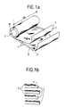
- the element (s) capacitive constituting the power capacitor are obtained by winding around a pin M of at least two films 1 having metallized zones 2 and on their opposite edges margins 3 not metallized.
- the metallized film used in the framework of the present invention is a polymer film plus particularly a bi-oriented polypropylene film.
- the polypropylene film is preferably, as shown in Figure 1B, a film rough. It can be rough on one side or rough on the two sides.
- this film, pre-treated corona was metallized using a metal such as aluminum in a vacuum metallization apparatus (resistivity of the metallization 1 to 5 ⁇ / ⁇ ).
- the two metallized films are wound by being offset from each other.
- a plastic film rough non-metallic is inserted between the two films on around 2 turns at the start and end of winding.
- the winding is realized around the spindle with a continuous servo of the profusion.
- this slaving will be such that we get an outside diameter coil on the mandrel M corresponding to an expansion about 15% compared to the weight thickness of the film metallic.
- expansion we mean the inter-space given by the winding between the layers.
- the profusion must be as consistent as possible.
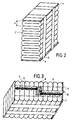
- the cylindrical capacitive element C thus obtained is extracted from the spindle M, it is flattened and put into press at a mechanical dimension corresponding to an overrun of 12% in the embodiment shown so as to obtain a flat element C 'as shown in FIG. 2.
- the use of flat elements makes it possible to obtain elements whose thickness e is perfectly controlled, that is to say elements whose expansion is completely determined.
- the flat elements bread in order to mechanically stabilize the dielectric film, is subjected to baking in a vacuum oven.
- this cooking is carried out at a temperature of about 80 ° C. under a vacuum of less than 10 -2 mmHg.
- the bread is left in the oven for 24 hours. Then, the temperature is brought down to 20 ° C and the breads are left for 16 hours before taking them out at room temperature.
- the shooping is carried out in a known manner by projection of a metal such as zinc onto a surface 6 (Zn layer thickness: 0.6 ⁇ m).
- This wiring operation is after cleaning the breads in order to eliminate zinc dust. This cleaning takes place for example by sending compressed air at a pressure of 4 bars.
- This wiring is made by first soldering a tinned copper foil on the middle part which aims to stiffen the entire bread. Then a copper braid 9 is welded on each element.
- the connections of the different elements are produced symmetrically at the top and bottom of the median for each half loaf so as to obtain a better distribution of currents.
- the capacitive elements are mounted in parallel. It is obvious for those skilled in the art that the capacitive elements can be mounted in parallel and / or in series.
- connection wire is soldered on part 8. This connection wire is intended to connect the capacitive bar to the connection terminal exterior, as shown in Figure 4.
- the first attempt is to unload in each bread a ballast energy of, for example, 62 Joules, which corresponds to the charge under 500 Volts of a 500 ⁇ F capacitor. This test makes it possible to carry out the short circuiting.
- Each loaf is charged at a continuous voltage corresponding to a gradient on the film of, for example, 200V / ⁇ m. This voltage is applied for a time of approximately 10 seconds. During this time, we therefore observe a number important of regenerations. If the regenerations are not stabilized after 30 seconds, the bread is considered unusable.
- a tank is used as a metallic parallelepiped housing, for example made of steel, stainless steel, aluminum.
- the metal housing allows easily ground the capacitor and is used to security reasons.
- the metal tank 11 is internally lined with plates 12, 13 and a holding plate 14 inserted subsequently, made of insulating materials for example polypropylene. These insulating material plates are used to electrically isolate the bun (s) from the tank.
- the plate 13, disposed at the bottom of the tank has a thickness of 10mm while the side profiles 12 have a thickness of 2mm.
- one or more breads of capacitive elements C ' are introduced into the tank metallic 11 and are wedged with one or more sets of plates 15 also made of insulating materials.
- the setting of the or breads inside the tank is essential so that the capacitive elements support vibrations.
- the plate holding 14 is then introduced.
- Two brackets 16 are then welded to the top of the tank to immobilize the assembly.
- the tank is provided with a cover 17 having an opening 18 for the passage of connection terminals 19 and impregnation.
- a liquid dielectric preferably a dielectric of the type vegetable such as rapeseed oil which has the main advantage not to damage the metallization and to penetrate very weakly polypropylene film.
- Adjuvants such as antioxidant and epoxy are added to preparations less than%; these adjuvants, in particular epoxy, allow the lifetime of the capacitors to be increased.
- Impregnation takes place in two phases.
- the condenser is first dried, preferably at a temperature of 50 ° C under a vacuum of 10 -2 mm of mercury. It is considered that the capacitor is properly dried when the torque 50 ° C / 10 -2 mm Hg has been reached for 24 hours.
- the liquid is degassed under vacuum, at 60 ° C., and it is decontaminated on earth materials or on an activated alumina column.
- the liquid is then admitted into the impregnation tank under vacuum at 10 -2 mm of mercury.
- the capacitive rolls are then impregnated by immersion.
- the capacitor is considered to be completely impregnated when the increase in capacity over eight hours does not exceed 1%.
- the vacuum is broken under nitrogen at atmospheric pressure and the temperature is then cut.
- the capacitors thus obtained are then subjected to classic end-of-production checks, such as leak tests, electrical temperature checks ambient and finishing treatments.
Landscapes
- Engineering & Computer Science (AREA)
- Power Engineering (AREA)
- Manufacturing & Machinery (AREA)
- Microelectronics & Electronic Packaging (AREA)
- Fixed Capacitors And Capacitor Manufacturing Machines (AREA)
- Ceramic Capacitors (AREA)
- Oscillators With Electromechanical Resonators (AREA)
- Electrical Discharge Machining, Electrochemical Machining, And Combined Machining (AREA)
- Curing Cements, Concrete, And Artificial Stone (AREA)
- Lubricants (AREA)
Claims (13)
- Verfahren zur Herstellung eines Leistungskondensators, gekennzeichnet durch die folgenden Verfahrensschritte:auf einen Dorn werden mindestens zwei metallbeschichtete Kunststoffolien mit einer Rippung bestehend aus lokalen Bereichen ohne Metallbeschichtung gewickelt, sodaß sich ein zylindrisches kapazitives Element ergibt, wobei das Wickeln unter kontinuierlicher Regelung des Füllgrads erfolgt;das zylindrische Element wird plattgedrückt, sodaß sich ein flaches Element mit einer vorbestimmten Dicke ergibt;das flache Element wird unter Vakuum ausgeheizt;die seitliche Metallisierung des flachen Elements wird hergestellt;die Kabelanschlüsse werden hergestellt;das flache Element wird in einen Behälter gebracht und mit einer dielektrischen Flüssigkeit imprägniert.
- Verfahren nach Anspruch 1, dadurch gekennzeichnet, daß am Anfang und am Ende der Wicklung eine nicht mit Metall beschichtete dielektrische Folie zwischen die beiden metallbeschichteten Folien eingefügt wird.
- Verfahren nach einem der Ansprüche 1 und 2,
dadurch gekennzeichnet, daß mehrere flache Elemente vor dem Ausheizen parallel angeordnet werden, um die gewünschte Kapazität zu erreichen. - Verfahren nach Anspruch 3, dadurch gekennzeichnet, daß die flachen Elemente in einem Metallbehälter unter Zwischenlage von Isolierschichten montiert werden, damit die kapazitiven Elemente Vibrationen standhalten.
- Verfahren nach einem der Ansprüche 1 bis 4,
dadurch gekennzeichnet, daß der Füllgrad des zylindrischen Elements etwa 15% beträgt. - Verfahren nach einem der Ansprüche 1 bis 5,
dadurch gekennzeichnet, daß der Füllgrad des flachen Elements etwa 12% beträgt. - Verfahren nach einem der Ansprüche 1 bis 6,
dadurch gekennzeichnet, daß die Kunststoffolie aus Polymermaterial ist und eine gewellte Oberfläche besitzt. - Verfahren nach Anspruch 7, dadurch gekennzeichnet, daß die Kunststoffolie eine Polypropylenfolie ist.
- Verfahren nach einem der Ansprüche 1 bis 8,
dadurch gekennzeichnet, daß die dielektrische Imprägnierflüssigkeit Rapsöl ist. - Verfahren nach einem der Ansprüche 1 bis 9,
dadurch gekennzeichnet, daß die Imprägnierung des Kondensators in zwei Phasen erfolgt, und zwar zuerst einer Trokkenphase unter Vakuum und dann einer Imprägnierphase durch Immersion unter Vakuum. - Verfahren nach Anspruch 10, dadurch gekennzeichnet, daß das Trocknen bei einer Temperatur von 50°C erfolgt.
- Verfahren nach einem der Ansprüche 10 und 11,
dadurch gekennzeichnet, daß das Trocknen und die Imprägnierung unter einem Vakuum von 10-2mm Quecksilber erfolgt. - Verfahren nach einem der Ansprüche 1 bis 12,
dadurch gekennzeichnet, daß man für die Wicklung eine metallbeschichtete Folie mit einem spezifischen Widerstand von zwischen 1 und 5 Ω pro Quadrat verwendet.
Applications Claiming Priority (2)
| Application Number | Priority Date | Filing Date | Title |
|---|---|---|---|
| FR9008227 | 1990-06-29 | ||
| FR9008227A FR2664089B1 (fr) | 1990-06-29 | 1990-06-29 | Condensateur de puissance. |
Publications (2)
| Publication Number | Publication Date |
|---|---|
| EP0465290A1 EP0465290A1 (de) | 1992-01-08 |
| EP0465290B1 true EP0465290B1 (de) | 1998-10-07 |
Family
ID=9398161
Family Applications (1)
| Application Number | Title | Priority Date | Filing Date |
|---|---|---|---|
| EP91401635A Expired - Lifetime EP0465290B1 (de) | 1990-06-29 | 1991-06-18 | Verfahren zum Herstellen eines Leistungskondensators |
Country Status (7)
| Country | Link |
|---|---|
| EP (1) | EP0465290B1 (de) |
| AT (1) | ATE172055T1 (de) |
| DE (1) | DE69130311T2 (de) |
| ES (1) | ES2121774T3 (de) |
| FI (1) | FI913178A7 (de) |
| FR (1) | FR2664089B1 (de) |
| WO (1) | WO1993011549A1 (de) |
Families Citing this family (4)
| Publication number | Priority date | Publication date | Assignee | Title |
|---|---|---|---|---|
| FR2664089B1 (fr) * | 1990-06-29 | 1996-04-12 | Europ Composants Electron | Condensateur de puissance. |
| DE4238643A1 (de) * | 1992-11-16 | 1994-05-19 | Siemens Matsushita Components | Elektrischer Kondensator mit kleiner Eigeninduktivität für die Energie-Elektronik |
| FR2701158B1 (fr) * | 1993-01-29 | 1995-03-10 | Lcc Cie Euro Composants Electr | Condensateur de puissance. |
| DE102004042307B3 (de) * | 2004-08-30 | 2006-02-02 | Siemens Ag | Hochspannungskondensator |
Family Cites Families (6)
| Publication number | Priority date | Publication date | Assignee | Title |
|---|---|---|---|---|
| DE1000530B (de) * | 1950-05-05 | 1957-01-10 | Siemens Ag | Elektrischer Kondensator, insbesondere Wickelkondensator |
| US3424957A (en) * | 1967-10-31 | 1969-01-28 | Gen Electric | Electrical capacitor and dielectric material therefor |
| IT1009956B (it) * | 1973-06-12 | 1976-12-20 | Gen Electric | Liquido impregnante costituito da estere stabilizzato |
| DE3029326A1 (de) * | 1980-08-01 | 1982-02-18 | Ero-Starkstrom Kondensatoren Gmbh, 8300 Landshut | Impraegnierter wickelkondensator |
| FR2579366A1 (fr) * | 1985-03-22 | 1986-09-26 | Europ Composants Electron | Condensateur a tres haute energie volumique et auto-cicatrisations controlees |
| FR2664089B1 (fr) * | 1990-06-29 | 1996-04-12 | Europ Composants Electron | Condensateur de puissance. |
-
1990
- 1990-06-29 FR FR9008227A patent/FR2664089B1/fr not_active Expired - Fee Related
-
1991
- 1991-06-18 AT AT91401635T patent/ATE172055T1/de not_active IP Right Cessation
- 1991-06-18 DE DE69130311T patent/DE69130311T2/de not_active Expired - Fee Related
- 1991-06-18 ES ES91401635T patent/ES2121774T3/es not_active Expired - Lifetime
- 1991-06-18 EP EP91401635A patent/EP0465290B1/de not_active Expired - Lifetime
- 1991-06-28 FI FI913178A patent/FI913178A7/fi unknown
- 1991-11-29 WO PCT/FR1991/000950 patent/WO1993011549A1/fr not_active Ceased
Also Published As
| Publication number | Publication date |
|---|---|
| FI913178A7 (fi) | 1991-12-30 |
| EP0465290A1 (de) | 1992-01-08 |
| DE69130311D1 (de) | 1998-11-12 |
| FR2664089A1 (fr) | 1992-01-03 |
| WO1993011549A1 (fr) | 1993-06-10 |
| DE69130311T2 (de) | 1999-03-04 |
| ATE172055T1 (de) | 1998-10-15 |
| FI913178A0 (fi) | 1991-06-28 |
| ES2121774T3 (es) | 1998-12-16 |
| FR2664089B1 (fr) | 1996-04-12 |
Similar Documents
| Publication | Publication Date | Title |
|---|---|---|
| US5043843A (en) | Film capacitor and method of making the same | |
| JPH0256803B2 (de) | ||
| EP0465290B1 (de) | Verfahren zum Herstellen eines Leistungskondensators | |
| US2731706A (en) | Manufacture of capacitors | |
| US3855507A (en) | Self heating capacitors | |
| US2709663A (en) | Electrical capacitors | |
| US3892023A (en) | Process of manufacturing a capacitor assembly | |
| CA1116706A (en) | Electrical capacitor with a pleated metallized portion and a starting portion wound about the lead wires | |
| GB2089569A (en) | Metallized-film Dual Capacitor | |
| KR100210560B1 (ko) | 전력콘덴서 | |
| FR2701158A1 (fr) | Condensateur de puissance. | |
| EP0001525A1 (de) | Kondensatoren mit Kunststoffilmen als Dielektra und Verfahren zu ihrer Herstellung | |
| US4945449A (en) | High voltage capacitor with high energy density | |
| FR2464546A1 (fr) | Condensateur a connexions a micro-bandes | |
| US4110878A (en) | Method for manufacturing an impregnated wound foil capacitor | |
| US575653A (en) | Electrical condenser | |
| EP0246134B1 (de) | Präzisionskondensator zur Einstellung der Nennkapazität | |
| US5258153A (en) | Method for the manufacture of stacked or wound type metallized polyethlene naphthalene film capacitors | |
| JP3284384B2 (ja) | 高圧コンデンサ | |
| KR102770028B1 (ko) | 고유전체 적용 다층 유전체 구조의 금속필름을 갖는 필름커패시터 | |
| JPH09260209A (ja) | 電力用コンデンサ | |
| JP2658614B2 (ja) | 金属化フィルムコンデンサの製造方法 | |
| JP3307135B2 (ja) | 電解コンデンサの製造方法 | |
| CH270972A (fr) | Procédé de fabrication d'un condensateur électrique. | |
| FR2553564A1 (fr) | Procede et dispositif correspondant pour ameliorer la rigidite dielectrique d'un isolement pour cables a courant continu |
Legal Events
| Date | Code | Title | Description |
|---|---|---|---|
| PUAI | Public reference made under article 153(3) epc to a published international application that has entered the european phase |
Free format text: ORIGINAL CODE: 0009012 |
|
| AK | Designated contracting states |
Kind code of ref document: A1 Designated state(s): AT CH DE DK ES FR GB IT LI NL SE |
|
| 17P | Request for examination filed |
Effective date: 19920125 |
|
| 17Q | First examination report despatched |
Effective date: 19931220 |
|
| GRAG | Despatch of communication of intention to grant |
Free format text: ORIGINAL CODE: EPIDOS AGRA |
|
| GRAG | Despatch of communication of intention to grant |
Free format text: ORIGINAL CODE: EPIDOS AGRA |
|
| GRAG | Despatch of communication of intention to grant |
Free format text: ORIGINAL CODE: EPIDOS AGRA |
|
| GRAH | Despatch of communication of intention to grant a patent |
Free format text: ORIGINAL CODE: EPIDOS IGRA |
|
| RAP1 | Party data changed (applicant data changed or rights of an application transferred) |
Owner name: THOMSON-CSF PASSIVE COMPONENTS |
|
| GRAH | Despatch of communication of intention to grant a patent |
Free format text: ORIGINAL CODE: EPIDOS IGRA |
|
| GRAA | (expected) grant |
Free format text: ORIGINAL CODE: 0009210 |
|
| AK | Designated contracting states |
Kind code of ref document: B1 Designated state(s): AT CH DE DK ES FR GB IT LI NL SE |
|
| PG25 | Lapsed in a contracting state [announced via postgrant information from national office to epo] |
Ref country code: NL Free format text: LAPSE BECAUSE OF FAILURE TO SUBMIT A TRANSLATION OF THE DESCRIPTION OR TO PAY THE FEE WITHIN THE PRESCRIBED TIME-LIMIT Effective date: 19981007 |
|
| REF | Corresponds to: |
Ref document number: 172055 Country of ref document: AT Date of ref document: 19981015 Kind code of ref document: T |
|
| REG | Reference to a national code |
Ref country code: CH Ref legal event code: EP |
|
| REF | Corresponds to: |
Ref document number: 69130311 Country of ref document: DE Date of ref document: 19981112 |
|
| REG | Reference to a national code |
Ref country code: ES Ref legal event code: FG2A Ref document number: 2121774 Country of ref document: ES Kind code of ref document: T3 |
|
| GBT | Gb: translation of ep patent filed (gb section 77(6)(a)/1977) |
Effective date: 19981209 |
|
| PG25 | Lapsed in a contracting state [announced via postgrant information from national office to epo] |
Ref country code: DK Free format text: LAPSE BECAUSE OF FAILURE TO SUBMIT A TRANSLATION OF THE DESCRIPTION OR TO PAY THE FEE WITHIN THE PRESCRIBED TIME-LIMIT Effective date: 19990107 |
|
| NLV1 | Nl: lapsed or annulled due to failure to fulfill the requirements of art. 29p and 29m of the patents act | ||
| PLBE | No opposition filed within time limit |
Free format text: ORIGINAL CODE: 0009261 |
|
| STAA | Information on the status of an ep patent application or granted ep patent |
Free format text: STATUS: NO OPPOSITION FILED WITHIN TIME LIMIT |
|
| 26N | No opposition filed | ||
| REG | Reference to a national code |
Ref country code: GB Ref legal event code: IF02 |
|
| PGFP | Annual fee paid to national office [announced via postgrant information from national office to epo] |
Ref country code: DE Payment date: 20020521 Year of fee payment: 12 |
|
| PGFP | Annual fee paid to national office [announced via postgrant information from national office to epo] |
Ref country code: SE Payment date: 20020522 Year of fee payment: 12 Ref country code: GB Payment date: 20020522 Year of fee payment: 12 |
|
| PGFP | Annual fee paid to national office [announced via postgrant information from national office to epo] |
Ref country code: CH Payment date: 20020605 Year of fee payment: 12 |
|
| PGFP | Annual fee paid to national office [announced via postgrant information from national office to epo] |
Ref country code: ES Payment date: 20020613 Year of fee payment: 12 |
|
| PGFP | Annual fee paid to national office [announced via postgrant information from national office to epo] |
Ref country code: FR Payment date: 20020621 Year of fee payment: 12 |
|
| PGFP | Annual fee paid to national office [announced via postgrant information from national office to epo] |
Ref country code: AT Payment date: 20020627 Year of fee payment: 12 |
|
| PG25 | Lapsed in a contracting state [announced via postgrant information from national office to epo] |
Ref country code: GB Free format text: LAPSE BECAUSE OF NON-PAYMENT OF DUE FEES Effective date: 20030618 Ref country code: AT Free format text: LAPSE BECAUSE OF NON-PAYMENT OF DUE FEES Effective date: 20030618 |
|
| PG25 | Lapsed in a contracting state [announced via postgrant information from national office to epo] |
Ref country code: SE Free format text: LAPSE BECAUSE OF NON-PAYMENT OF DUE FEES Effective date: 20030619 Ref country code: ES Free format text: LAPSE BECAUSE OF NON-PAYMENT OF DUE FEES Effective date: 20030619 |
|
| PG25 | Lapsed in a contracting state [announced via postgrant information from national office to epo] |
Ref country code: LI Free format text: LAPSE BECAUSE OF NON-PAYMENT OF DUE FEES Effective date: 20030630 Ref country code: CH Free format text: LAPSE BECAUSE OF NON-PAYMENT OF DUE FEES Effective date: 20030630 |
|
| PG25 | Lapsed in a contracting state [announced via postgrant information from national office to epo] |
Ref country code: DE Free format text: LAPSE BECAUSE OF NON-PAYMENT OF DUE FEES Effective date: 20040101 |
|
| EUG | Se: european patent has lapsed | ||
| GBPC | Gb: european patent ceased through non-payment of renewal fee |
Effective date: 20030618 |
|
| REG | Reference to a national code |
Ref country code: CH Ref legal event code: PL |
|
| PG25 | Lapsed in a contracting state [announced via postgrant information from national office to epo] |
Ref country code: FR Free format text: LAPSE BECAUSE OF NON-PAYMENT OF DUE FEES Effective date: 20040227 |
|
| REG | Reference to a national code |
Ref country code: FR Ref legal event code: ST |
|
| REG | Reference to a national code |
Ref country code: ES Ref legal event code: FD2A Effective date: 20030619 |
|
| PG25 | Lapsed in a contracting state [announced via postgrant information from national office to epo] |
Ref country code: IT Free format text: LAPSE BECAUSE OF NON-PAYMENT OF DUE FEES;WARNING: LAPSES OF ITALIAN PATENTS WITH EFFECTIVE DATE BEFORE 2007 MAY HAVE OCCURRED AT ANY TIME BEFORE 2007. THE CORRECT EFFECTIVE DATE MAY BE DIFFERENT FROM THE ONE RECORDED. Effective date: 20050618 |