EP0465714A1 - Panne de fer à souder en étrier céramique - Google Patents
Panne de fer à souder en étrier céramique Download PDFInfo
- Publication number
- EP0465714A1 EP0465714A1 EP90113492A EP90113492A EP0465714A1 EP 0465714 A1 EP0465714 A1 EP 0465714A1 EP 90113492 A EP90113492 A EP 90113492A EP 90113492 A EP90113492 A EP 90113492A EP 0465714 A1 EP0465714 A1 EP 0465714A1
- Authority
- EP
- European Patent Office
- Prior art keywords
- soldering
- ceramic
- resistors
- edge
- ceramic substrate
- Prior art date
- Legal status (The legal status is an assumption and is not a legal conclusion. Google has not performed a legal analysis and makes no representation as to the accuracy of the status listed.)
- Granted
Links
Images
Classifications
-
- B—PERFORMING OPERATIONS; TRANSPORTING
- B23—MACHINE TOOLS; METAL-WORKING NOT OTHERWISE PROVIDED FOR
- B23K—SOLDERING OR UNSOLDERING; WELDING; CLADDING OR PLATING BY SOLDERING OR WELDING; CUTTING BY APPLYING HEAT LOCALLY, e.g. FLAME CUTTING; WORKING BY LASER BEAM
- B23K3/00—Tools, devices or special appurtenances for soldering, e.g. brazing, or unsoldering, not specially adapted for particular methods
- B23K3/04—Heating appliances
- B23K3/047—Heating appliances electric
- B23K3/0471—Heating appliances electric using resistance rod or bar, e.g. carbon silica
Definitions
- the invention relates to a ceramic soldering bracket for soldering by means of resistance heating, in particular for reflow soldering of electronic components, which generally have a large number of connection legs.
- soldering brackets used in soldering devices. Pressing the soldering partners and the heat transfer for the soldering process or the generation of the necessary heat are usually done by the soldering clip.
- the common embodiments are designed so that the connecting legs arranged next to one another in a row are pressed and heated by a strip-shaped soldering clip, for example a U-shaped component with a long crosspiece. If the soldering clip is made of an electrically conductive material, the heat being generated by resistance heating in the soldering clip, there is a risk of damage to an electronic component due to the voltage drop within the soldering clip occurring between different connection pins. Currents generated in this way in the component can have disadvantageous consequences.
- soldering bracket which has a ceramic strip or ceramic rod glued into a groove in the soldering bracket. The contact between the connection leg and the soldering bracket is made via this ceramic strip. Due to the low ohmic resistances of this soldering clip, large electrical currents must flow through the soldering clip to generate the necessary amount of heat. This requires complex switching and control technology and an equally complex power supply. Furthermore, extremely low-impedance connection technology is necessary for large currents. The principle here is that the heat should arise in the soldering iron and not at the electrical connections of the soldering iron.
- thermocouples attempt to control or regulate the temperature along the edge of the soldering iron.
- the invention has for its object to provide a ceramic soldering bracket available, which can be used by means of a soldering edge for soldering electronic components without voltage drop between individual connection pins and which provides the heat required for the soldering process with good heat conductivity and with low losses to the soldering edge.
- the invention is based on the knowledge that an all-ceramic and thus electrically non-conductive soldering clip achieves further substantial advantages if it consists of a good heat-conducting ceramic material. This applies particularly to the soldering edge.
- the amount of heat is applied in the immediate vicinity of the soldering edge on the flat ceramic substrate at least one also flat electrical resistance.
- the electrical resistance can be applied using thin-film or thick-film technology.
- An advantageous embodiment of the invention provides for the ceramic substrate to be designed in the form of a rectangular disk.
- the two opposite large surfaces of the disc serve to hold the ceramic substrate, for example by means of a chuck and to apply the resistors, a narrow side of the ceramic substrate representing the soldering edge which is pressed onto the connection pins.
- the resistors used to generate the process heat are positioned in the area of the soldering edge.
- a flat metal layer is applied to the large areas of the rectangular disk. This metal layer can be applied simultaneously with the resistors.
- a predetermined temperature profile is required at the soldering edge, this can be generated by means of trimming resistors, which are connected between the individual resistors for generating the process heat, via heat outputs of the individual resistors which can be set differently.
- An advantageous embodiment of the invention provides a thermal resistance within the ceramic soldering bow in the form of a row of holes, which is represented parallel to the soldering edge on the side of the resistors opposite the soldering edge by adjacent holes. This row of holes reduces the effective heat-conducting cross section of the soldering clip in the direction of the holder. If necessary, several rows of holes can be laid one after the other.
- Bores that have been made to reduce the heat-conducting cross section can advantageously be used simultaneously for plated-through holes.
- An advantageous choice of material for the ceramic substrate preferably for the area of the soldering edge, consists in the use of a ceramic with high thermal conductivity.
- the use of beryllium oxide or aluminum nitride is particularly suitable here.
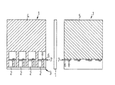
- a ceramic substrate 1 is shown in the front view, in the side view and in the rear view.
- the all-ceramic soldering bracket no voltage drop occurs when electronic components are soldered between their individual connection pins. This is achieved by using a ceramic that is not electrically conductive.
- the ceramic substrate consists of a good heat-conducting ceramic, such as aluminum nitride. Since there is no voltage drop at the soldering edge of an all-ceramic soldering clip, these soldering clips can be designed for higher operating voltages. An interpretation regarding the operating voltage and the heating power to be applied by a resistor can be carried out with expert knowledge.
- the thin film or thick film technique used to apply resistance to the ceramic substrate is characterized either by vapor deposition or sputtering, or by screen printing processes. Structures applied using thick-film technology usually contain glass. Ceramic soldering brackets are thus produced by methods customary in electrical engineering for coating and structuring ceramic substrates.
- the ceramic substrate 1 is shown with a thickness that remains the same over the entire height, the lower edge representing the soldering edge 3.
- four resistors 2 have been applied by thin-film technology, the electrical contact being made through the metal foil 4 on the left and right of the resistors 2.
- the electrical connection to the metal layer 5 located on the rear side is established by means of the through contact 8.
- clamping jaws can be used, which at the same time represent the electrical leads for the soldering iron.
- the jaws would grip the solder bar in the upper part and ensure the electrical supply by contact with the metal foils 4, 5.
- the row of holes 7, which consists of a plurality of holes 6, provides an increased thermal resistance, so that a preferred direction of heat flow to the soldering edge 3 prevails.
- a thermistor can be applied at the same time during the coating process for the resistors 2.
- the soldering edge 3 should remain uncoated. Although there is the possibility of covering the entire structure applied by a glaze layer and thus electrically isolating it, it is not sensible to apply the resistors to the soldering edge 3.
- the resistors 2 must be flat and thus applied to the broad side of the ceramic substrate 1.
- the resistors 2, which are used for heating, are arranged at a short distance along the soldering edge and are electrically connected in parallel.
- the ceramic substrate 1 represents the actually load-bearing component.
- a narrow side is used as the soldering edge 3 in the planar configuration of the ceramic substrate 1.
- the electrical conductors are not load-bearing parts.
- the use of a ceramic material, such as aluminum nitride, already mentioned ensures a thermal conductivity that corresponds to that of conventionally used metals. Ceramic fillers, for example, have a thermal conductivity of at least 10 W / mK and, depending on the modification, aluminum nitride has a thermal conductivity of 30 - 150 W / mK.
Landscapes
- Engineering & Computer Science (AREA)
- Mechanical Engineering (AREA)
- Resistance Heating (AREA)
- Manufacturing Of Electrical Connectors (AREA)
- Details Of Resistors (AREA)
- Ceramic Products (AREA)
Priority Applications (5)
| Application Number | Priority Date | Filing Date | Title |
|---|---|---|---|
| AT90113492T ATE120678T1 (de) | 1990-07-13 | 1990-07-13 | Keramischer lötbügel. |
| EP90113492A EP0465714B1 (fr) | 1990-07-13 | 1990-07-13 | Panne de fer à souder en étrier céramique |
| DE59008864T DE59008864D1 (de) | 1990-07-13 | 1990-07-13 | Keramischer Lötbügel. |
| US07/719,757 US5221819A (en) | 1990-07-13 | 1991-06-24 | Ceramic soldering element |
| JP3197069A JPH04231173A (ja) | 1990-07-13 | 1991-07-10 | セラミックろう付け具 |
Applications Claiming Priority (1)
| Application Number | Priority Date | Filing Date | Title |
|---|---|---|---|
| EP90113492A EP0465714B1 (fr) | 1990-07-13 | 1990-07-13 | Panne de fer à souder en étrier céramique |
Publications (2)
| Publication Number | Publication Date |
|---|---|
| EP0465714A1 true EP0465714A1 (fr) | 1992-01-15 |
| EP0465714B1 EP0465714B1 (fr) | 1995-04-05 |
Family
ID=8204215
Family Applications (1)
| Application Number | Title | Priority Date | Filing Date |
|---|---|---|---|
| EP90113492A Expired - Lifetime EP0465714B1 (fr) | 1990-07-13 | 1990-07-13 | Panne de fer à souder en étrier céramique |
Country Status (5)
| Country | Link |
|---|---|
| US (1) | US5221819A (fr) |
| EP (1) | EP0465714B1 (fr) |
| JP (1) | JPH04231173A (fr) |
| AT (1) | ATE120678T1 (fr) |
| DE (1) | DE59008864D1 (fr) |
Families Citing this family (4)
| Publication number | Priority date | Publication date | Assignee | Title |
|---|---|---|---|---|
| US5650081A (en) * | 1994-06-29 | 1997-07-22 | Zevatech, Inc. | Thermode solder blade with electric heater greater than four ohms |
| DE10307832B4 (de) * | 2003-02-25 | 2008-01-17 | Forschungszentrum Karlsruhe Gmbh | Werkzeug in Form eines heizbaren Stiftes |
| US7964883B2 (en) * | 2004-02-26 | 2011-06-21 | Lighting Science Group Corporation | Light emitting diode package assembly that emulates the light pattern produced by an incandescent filament bulb |
| DE102006024281B4 (de) * | 2006-05-24 | 2012-12-06 | Melzer Maschinenbau Gmbh | Verwendung eines Verfahrens zum löttechnischen Verbinden von leitfähigen Bauteilen |
Citations (2)
| Publication number | Priority date | Publication date | Assignee | Title |
|---|---|---|---|---|
| US4412123A (en) * | 1980-05-09 | 1983-10-25 | Bell Telephone Laboratories, Incorporated | Laminated electric heat generating member for reflow soldering devices |
| EP0357977A2 (fr) * | 1988-09-07 | 1990-03-14 | Siemens Aktiengesellschaft | Dispositif de brasage avec au moins une électrode à étrier à chauffage par chaleur de résistance |
Family Cites Families (15)
| Publication number | Priority date | Publication date | Assignee | Title |
|---|---|---|---|---|
| US2886854A (en) * | 1955-01-07 | 1959-05-19 | Albert W Franklin | Resistor grid and method of making |
| US3230338A (en) * | 1962-07-02 | 1966-01-18 | Ibm | Selective heating apparatus |
| US3576969A (en) * | 1969-09-02 | 1971-05-04 | Ibm | Solder reflow device |
| US3775725A (en) * | 1970-04-30 | 1973-11-27 | Hokuriku Elect Ind | Printed resistor |
| US3786228A (en) * | 1971-12-15 | 1974-01-15 | Roesch K Inc | Electric soldering iron tip |
| US3991297A (en) * | 1975-02-27 | 1976-11-09 | Bell Telephone Laboratories, Incorporated | Electrically heated soldering device |
| US4297670A (en) * | 1977-06-03 | 1981-10-27 | Angstrohm Precision, Inc. | Metal foil resistor |
| US4315128A (en) * | 1978-04-07 | 1982-02-09 | Kulicke And Soffa Industries Inc. | Electrically heated bonding tool for the manufacture of semiconductor devices |
| DE2847482A1 (de) * | 1978-11-02 | 1980-05-14 | Degussa | Schnellaufheizender loetkolben |
| JPS60136391A (ja) * | 1983-12-26 | 1985-07-19 | 株式会社日立製作所 | 回路基板 |
| JPS61209767A (ja) * | 1985-03-14 | 1986-09-18 | Toshiba Corp | はんだごて |
| JPS63153829A (ja) * | 1986-12-18 | 1988-06-27 | Toshiba Corp | ボンデイング用加熱ブロツク |
| JPH0677828B2 (ja) * | 1988-11-28 | 1994-10-05 | 株式会社トーキン | 電気半田こて用加熱素子組立体及び電気半田こて |
| JP2677642B2 (ja) * | 1988-12-15 | 1997-11-17 | 株式会社東芝 | 加熱ヘッドおよび電子部品の実装方法 |
| EP0377873B1 (fr) * | 1989-01-10 | 1994-08-10 | Siemens Aktiengesellschaft | Dispositif de brasage avec au moins une électrode à étrier à chauffage par résistance électrique |
-
1990
- 1990-07-13 DE DE59008864T patent/DE59008864D1/de not_active Expired - Fee Related
- 1990-07-13 AT AT90113492T patent/ATE120678T1/de active
- 1990-07-13 EP EP90113492A patent/EP0465714B1/fr not_active Expired - Lifetime
-
1991
- 1991-06-24 US US07/719,757 patent/US5221819A/en not_active Expired - Fee Related
- 1991-07-10 JP JP3197069A patent/JPH04231173A/ja active Pending
Patent Citations (2)
| Publication number | Priority date | Publication date | Assignee | Title |
|---|---|---|---|---|
| US4412123A (en) * | 1980-05-09 | 1983-10-25 | Bell Telephone Laboratories, Incorporated | Laminated electric heat generating member for reflow soldering devices |
| EP0357977A2 (fr) * | 1988-09-07 | 1990-03-14 | Siemens Aktiengesellschaft | Dispositif de brasage avec au moins une électrode à étrier à chauffage par chaleur de résistance |
Non-Patent Citations (1)
| Title |
|---|
| IBM TECHNICAL DISCLOSURE BULLETIN. vol. 11, no. 8, Januar 1969, NEW YORK US Seite 1026 N.F. JENSEN: "SELF-LEVELING SOLDERING TOOL" * |
Also Published As
| Publication number | Publication date |
|---|---|
| ATE120678T1 (de) | 1995-04-15 |
| US5221819A (en) | 1993-06-22 |
| JPH04231173A (ja) | 1992-08-20 |
| EP0465714B1 (fr) | 1995-04-05 |
| DE59008864D1 (de) | 1995-05-11 |
Similar Documents
| Publication | Publication Date | Title |
|---|---|---|
| DE2840514C2 (fr) | ||
| DE102007028791B4 (de) | Thermoelektrische Umwandlungsvorrichtung und Herstellungsverfahren dafür | |
| EP1450404B1 (fr) | Assemblage en contact à pression avec module semi-conducteur de puissance | |
| DE2041497B2 (de) | Verfahren zum Herstellen eines Halbleiterbauelementes | |
| DE2260722A1 (de) | Loetkolbenspitze | |
| DE102007050405B4 (de) | Elektrische Leistungskomponente, insbesondere Leistungshalbleiter-Modul, mit einer Kühlvorrichtung und Verfahren zum flächigen und wärmeleitenden Anbinden einer Kühlvorrichtung an eine elektrische Leistungskomponente | |
| DE102015224020B4 (de) | Thermoelektrisches Modul | |
| DE1961042C3 (de) | Halbleiterbauelement | |
| EP0465714B1 (fr) | Panne de fer à souder en étrier céramique | |
| DE7223394U (de) | Gedruckte elektrische Schaltungsanordnung | |
| DE1514562B2 (de) | Anordnung zur herstellung eines halbleiter-bauelementes | |
| DE10297291T5 (de) | Stossstrom-Chipwiderstand | |
| DE2528000B2 (de) | Verfahren zur Herstellung einer Lötfläche relativ großer Abmessungen | |
| DE4206365C1 (fr) | ||
| DE102008015376B4 (de) | Elektrische Verbindung | |
| DE1465736B2 (de) | Funktionsblock, insbesondere für datenverarbeitende Anlagen | |
| DE102004019568B4 (de) | Leistungshalbleitermodul mit einem Substrat | |
| DE102019115573B4 (de) | Leistungselektronische Schalteinrichtung und Verfahren zur Herstellung | |
| DE10134187A1 (de) | Kühleinrichtung für Halbleitermodule | |
| DE9319473U1 (de) | Hybridschaltungsanordnung | |
| DE3926238C2 (de) | Halbleiter-Bauelement | |
| EP0268935A1 (fr) | Circuit intégré enfichable perpendiculairement à connexions en ligne | |
| DE2453968C2 (de) | Kuehlfederleiste fuer direkt steckbare schicht- und/oder miniprintschaltungen | |
| DE102018207360B4 (de) | Stromschiene, verfahren für deren herstellung und leistungsmodul, welches selbige aufweist | |
| DE102019212638B4 (de) | Verfahren zur Fertigung und Aufbringung eines leistungselektronischen Moduls auf einen Kühlkörper und damit erhaltene Anordnung |
Legal Events
| Date | Code | Title | Description |
|---|---|---|---|
| PUAI | Public reference made under article 153(3) epc to a published international application that has entered the european phase |
Free format text: ORIGINAL CODE: 0009012 |
|
| 17P | Request for examination filed |
Effective date: 19901205 |
|
| AK | Designated contracting states |
Kind code of ref document: A1 Designated state(s): AT BE CH DE FR GB IT LI NL |
|
| 17Q | First examination report despatched |
Effective date: 19930209 |
|
| GRAA | (expected) grant |
Free format text: ORIGINAL CODE: 0009210 |
|
| AK | Designated contracting states |
Kind code of ref document: B1 Designated state(s): AT BE CH DE FR GB IT LI NL |
|
| PG25 | Lapsed in a contracting state [announced via postgrant information from national office to epo] |
Ref country code: IT Free format text: LAPSE BECAUSE OF FAILURE TO SUBMIT A TRANSLATION OF THE DESCRIPTION OR TO PAY THE FEE WITHIN THE PRE;WARNING: LAPSES OF ITALIAN PATENTS WITH EFFECTIVE DATE BEFORE 2007 MAY HAVE OCCURRED AT ANY TIME BEFORE 2007. THE CORRECT EFFECTIVE DATE MAY BE DIFFERENT FROM THE ONE RECORDED.SCRIBED TIME-LIMIT Effective date: 19950405 Ref country code: FR Effective date: 19950405 Ref country code: NL Free format text: LAPSE BECAUSE OF NON-PAYMENT OF DUE FEES Effective date: 19950405 Ref country code: GB Effective date: 19950405 Ref country code: BE Effective date: 19950405 |
|
| REF | Corresponds to: |
Ref document number: 120678 Country of ref document: AT Date of ref document: 19950415 Kind code of ref document: T |
|
| REF | Corresponds to: |
Ref document number: 59008864 Country of ref document: DE Date of ref document: 19950511 |
|
| PG25 | Lapsed in a contracting state [announced via postgrant information from national office to epo] |
Ref country code: AT Effective date: 19950713 |
|
| PG25 | Lapsed in a contracting state [announced via postgrant information from national office to epo] |
Ref country code: CH Effective date: 19950731 Ref country code: LI Effective date: 19950731 |
|
| EN | Fr: translation not filed | ||
| NLV1 | Nl: lapsed or annulled due to failure to fulfill the requirements of art. 29p and 29m of the patents act | ||
| GBV | Gb: ep patent (uk) treated as always having been void in accordance with gb section 77(7)/1977 [no translation filed] |
Effective date: 19950405 |
|
| PLBE | No opposition filed within time limit |
Free format text: ORIGINAL CODE: 0009261 |
|
| STAA | Information on the status of an ep patent application or granted ep patent |
Free format text: STATUS: NO OPPOSITION FILED WITHIN TIME LIMIT |
|
| REG | Reference to a national code |
Ref country code: CH Ref legal event code: PL |
|
| 26N | No opposition filed | ||
| PGFP | Annual fee paid to national office [announced via postgrant information from national office to epo] |
Ref country code: DE Payment date: 20030916 Year of fee payment: 14 |
|
| PG25 | Lapsed in a contracting state [announced via postgrant information from national office to epo] |
Ref country code: DE Free format text: LAPSE BECAUSE OF NON-PAYMENT OF DUE FEES Effective date: 20050201 |